MXIC MX97102 Datasheet

FEATURES
MX97102
ISDN S/T CONTROLLER
• Pin-to-Pin and Register-to-Register compatible with
Siemens 2186
• Full duplex 2B+D ISDN S/T Transceiver according to
CCITT I.430
• GCI digital interface
• 3 types of 8-bit CPU interface
• Receive timing recovery with adaptively switched
thresholds
• E-channel Monitoring
GENERAL DESCRIPTIONS
MX97102 implements the 4-wire S/T interface used to
link voice/data terminals to an ISDN. It is designed for
the user site of the ISDN-basic access, two 64kbit/s B
channels and a 16kbit/s D channel.
MX97102 can be mainly divided into three portions according to their interfaces. Except these three interf ace
functions, it also provides the LAPD controller which
handles the HDLC packets of the ISDN D-channel for
the associated microprocessor.
The first, S/T interface controller , pro vides all electrical
and logical functions of the S/T interface, such as S/T
transceiver, activation/deactivation, timing recovery,
• Programmable SDS1,SDS2
• D-channel access control
• LAPD(HDLC) support with FIFO(2x64) buffers
• Activation/Deactivation
• Multiframing with S and Q bit access
• CPU access to B and IC channels
• Watchdog timer
• Package types : P-LCC-44, P-LQFP-64
multiframe S and Q channels, and D-channel access
and priority control for communicating with remote
equipments.
The Second is the microprocessor interface controller
which offers the registers compatible with Siemens
PSB2186, provides three types of microprocessor interface, such as Motorola bus mode, Intel multiplexed
mode and Intel non-multiplex ed mode.
The last portion is the GCI interface controller which is
used to connect different voice/data application modules for local digital data exchangements.
PIN CONFIGURATION
44-PLCC 64-PLQFP
NCNCNCNCPAD7
484746454443424140393837363534
49
50
51
52
53
54
55
56
57
58
59
60
61
62
63
64
123456789101112131415
NCNCNCNCNC
PSDS1
PSDS2
PRST
PA5(EAW)
VSSD
PDCL
PFSC1
NC
VSSD
ECHO
PA4
PA1
PA2
PAD7
PAD6
PAD5
PAD4
PAD3
PAD2
PAD1
PAD0
PA0
64440
7
12
17
18 23 28
NC
NC
PA3
1
MX97102
PBCL
VSSD
PINTN
VSSA
PXTAL2
PXTAL1
39
34
29
PSR2
PRDN(DS)
PWRN(R/W)
PCSN
PALE
PIDP1
PIDP0
PSX2
PSX1
VDD
NC
NC
PSR1
NC
PA2
PA1
PSDS1
PSDS2
PRST
PA5(EAW)
NC
VSSD
PDCL
PFSC1
NC
VSSD
ECHO
PA4
PA3
P/N:PM0473 REV. 2.5, SEP. 05, 2000
1
PAD6
PAD5
MX97102
PBCL
VSSD
PAD4
PINTN
PAD3
NC
PAD2
VSSA
PAD1
PXTAL2
PAD0NCNCNCNC
NC
PSR2NCPSR1
PXTAL1
33
16
32
31
30
29
28
27
26
25
24
23
22
21
20
19
18
17
NC
NC
PA0
PRDN(D5)
PWRN(R/W)
PCSN
PALE
PIDP1
PIDP0
PSX2
PSX1
VDD
NC
NC
NC
NC
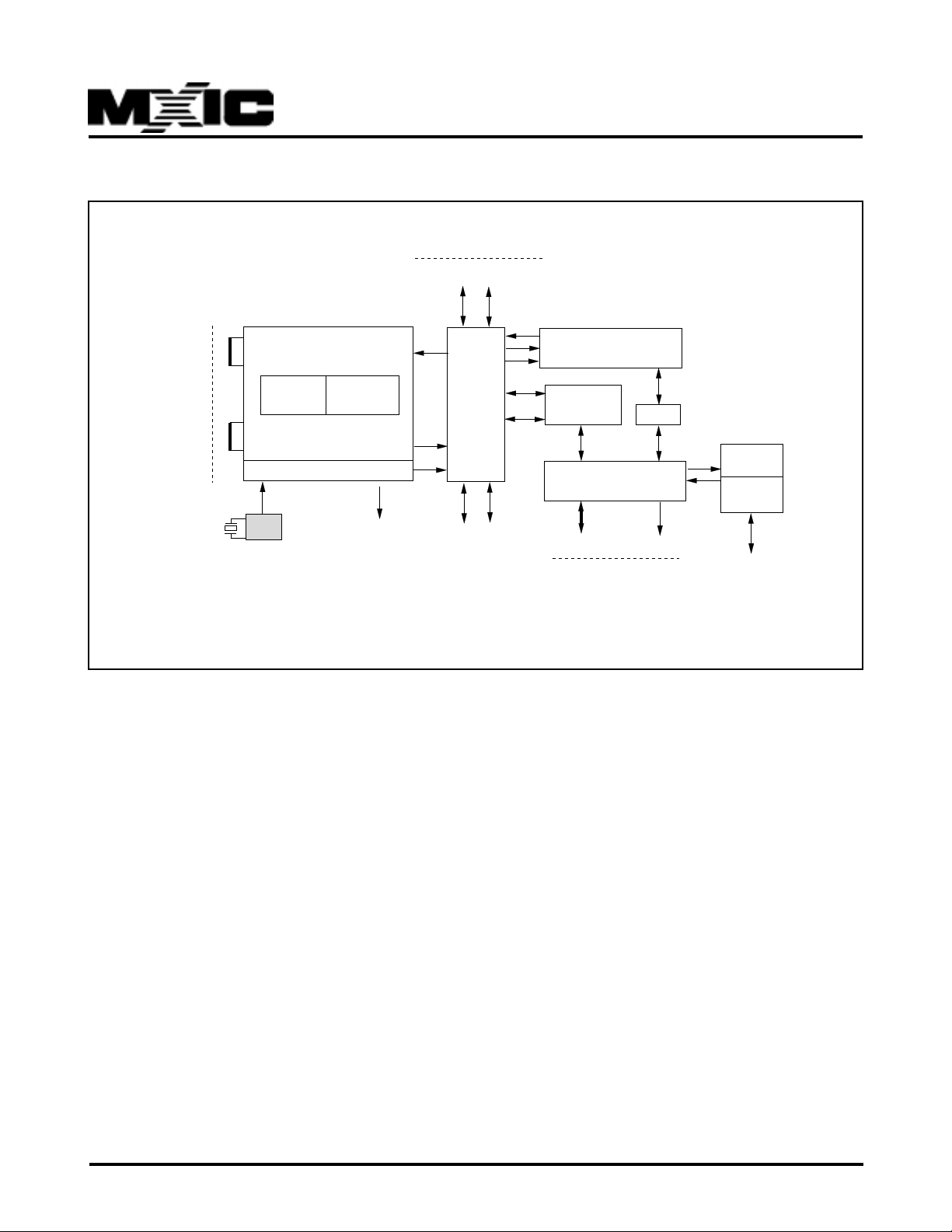
BLOCK DIAGRAM
S/T Interface
MX97102
Control and Data
Interface signals
PIDP0 PIDP1
7.68MHZ
Transmitter
Multiframe
control
Receiver
OSC
LAP-D
Activation/
Deactivation
DPLL
ECHO
GCI
Interface
PDCL PFSC1
B-channel
Switching
uP
Interface
microprocessor interface
FIGURE 2: FUNCTIONAL BLOCK DIAGRAM
FIFO
WATCH
DOG
RESET
SOURCE
PINTN
PRST
P/N:PM0473
REV. 2.5, SEP. 05, 2000
2

MX97102
PIN DESCRIPTION (44-PIN)
TABLE 1: MX97102 PIN DESCRIPTIONS
LQFP PLCC
PAD# PAD# PIN NAME I/O DESCRIPTION
37 41 PAD0(D0) Multiplexed Bus Mode:Address/data b us from the CPU system to this devic
38 42 PAD1(D1) ,and data between the CPU system and this device.
39 43 PAD2(D2) Non-Multiplexed Bus Mode:Data bus between the CPU system and this
40 44 PAD3(D3) I/O device.
41 1 PAD4(D4)
42 2 PAD5(D5)
43 3 PAD6(D6)
44 4 PAD7(D7)
27 37 PCSN I ChipSelect:A logic "LOW" enable this device for a read/write operation.
28 38 PWRN(R/W) I Read/Write:A logic "HIGH" indicates a valid read operation by CPU.
A logic "LOW" indicates a valid write operation by CPU.(Motorola bus
mode) Write:A logic "LOW" indicates a write operation.(Intel bus mode)
29 39 PRDN(DS) I Data Strobe:
The rising edge marks the end of a valid read or write operation (Motorola
bus mode). Read:A logic "LOW" indicates a read operation.(Intel bus mode)
8 23 PINTN Open Interrupt Request:The signal is a logic "LOW" when this device
requests an Drain interrupt. It is an open drain output.
1~5, 14 NC
9,13,15 19,20 No used.
17~20 29,30
31~36
45~49
56,60
26 36 PALE I Address Latch Enable:A logic "HIGH" indicates an address on the address/
data bus(Multiplex ed b us type only). ALE also selects the micro-processor
interface type (multiplexed or non-multiplexed).
54 9 PRST I/O Reset:A logic "HIGH" on this input forces this device into reset state. The
minimum pulse length is four DCL-clock periods or four ms. If the terminal
specific functions are enabled,this device may also output a reset signal.
59 13 PFSC1 O(I) Frame Sync 1:Frame sync output. Logic "HIGH" during channel 0 on the
GCI interface. This pin becomes Input if Test Mode is programmed (register
ADF1).
58 12 PDCL O(I) Data Clock:Clock of frequency, 1536kHz output, equals to twice the GCI
data rate.
This pin becomes Input if Test Mode is programmed (register ADF1)
62 16 ECHO O This pin output the Echo bit from the receiving line.
P/N:PM0473
REV. 2.5, SEP. 05, 2000
3

MX97102
TABLE 1: MX97102 PIN DESCRIPTIONS(Continued)
LQFP PLCC
PAD# PAD# PIN NAME I/O DESCRIPTION
(non-multiplex ed b us mode)
30 40 PA0 I Address Bit 0
51 6 PA1 I Address Bit 1
50 5 PA2 I Address Bit 2
64 18 PA3 I Address Bit 3
63 17 PA4 I Address Bit 4
55 10 PA5(EAW) I Address Bit 5; External Awake, when terminal specific function en
abled, this pin is used as an external awak e line. If a falling edge on this
input is detected, it generates an interrupt and a reset pulse.
7 22 PBCL O Bit Clock:Clock of frequency 768kHz equal to the GCI data rate.
52,53 7,8 PSDS1,2 O Serial Data Strobe 1&2 : programmable strobe signals , selecting either
one or two B or IC channels on GCI interface, is supplied via this line.
(registers ADF2,4)
6,57,61 11, 15
21 VSSD - Digital ground
10 24 VSSA - Analog ground
21 31 VDD - Power supply (5V±5%)
12 26 PXTAL1 I Connection for crystal or external clock input.
11 25 PXTAL2 O Connection for external crystal. Left unconnected if external clock is
used.
14 27 PSR2
16 28 PSR1 I S-Bus Receiver Input
22 32 PSX1 S-Bus Transmitter Output(positive)
23 33 PSX2 O S-Bus Tr ansmitter Output(negative)
24 34 PIDP0(DD) GCI-Data Port 0 (DD)
25 35 PIDP1(DU) I / O GCI-Data Port 1 (DU)
Open drain without internal pull-up resister or push-pull.
ABSOLUTE MAXIMUM RATINGS
TABLE 2: ABSOLUTE MAXIMUM RATINGS
RATING VALUE
Maximum Supply Voltage (VDD) 6V
DC Input Voltage on any pin -0.4Vto VDD+0.4V
Storage Temperature Range -55°C to 150°C
Operating Free Air Temperature Range 0°C to 70°C
P/N:PM0473
REV. 2.5, SEP. 05, 2000
4

MX97102
DC CHARACTERISTICS
TABLE 3: DC CHARACTERISTICS
Temperature from 0 to 70°C; VDD = 5V±5%, VSSA = 0V, VSSD = 0V
Symbol Parameter Conditions Min. Value Max. V alue Unit Remarks
VIL L-input voltage -0.4 0.8 V
VIH H-input voltage 2.0 VDD+0.4 V All pins except
VOL L-output voltage IOL= 2mA 0.45 V PSX1, PSX2,
VOL1 L-output voltage (IDP0) IOL= 7mA 0.45 V PSR1, PSR2
VOH H-output voltage IOH= -400uA 2.4 V
VOH H-output voltage IOH= -100uA
VDD-0.75 V
ILI Input leakage current 0<VIN<VDD to 0V ±10 All pins except
BCL, PSX1,2,
ILO Output leakage current 0<VOUT<VDD to 0V ±10 uA PSR1,2, PA0,
PA1, PA3, PA4
ILIPD Input leakage current,
internal pull-down 0<VIN<VDD to 0V 120 uA PA0, PA1, PA3,
PA4, BCL
VX Absolute value of RL = 50ohm 2.03 2.31
output pulse amplitude RL = 400ohm 2.35 2.65 V PSX1, PSX2
(VSX2 - VSX1)
IX Transmitter out-
put current RL = 5.6ohm 7.5 13.4 mA
RX Transmitter out- Inactive or during
put impedance binary one 10 kohm
during binary zero 0 ohm
RL = 50ohm
VSR1 Receiver output voltage IO < 5uA 2.35 2.63 V PSR1, PSR2
VTR Receiver threshold Dependent on
voltage (VSR2 - VSR1) peak level 225 375 mV
P/N:PM0473
REV. 2.5, SEP. 05, 2000
5
MX97102
AC CHARA CTERICS
TABLE 4: CRYSTAL SPECIFICATION
PARAMETER SYMBOL Limit values UNIT
Frequency f 7.680 MHz
Frequency calibration tolerance max. 100 ppm
Load capacitance CL max. 50 pF
Oscillator mode fundamental
XTAL1 Clock Characteristics (external oscillator
input)
TABLE 5: CLOCK CHARACTERISTICS
Parameter Limit values
min. max.
Duty cycle 1:2 2:1
Temperature from 0 to 70°C, VDD = 5V±5%
Inputs are driven to 2.4V for a logical "1" and to 0.4V
for a logical "0" . Timing measurements are made at
2.0V for a logical "1" and 0.8V f or a logical "0". The A Ctesting output is loaded with a 150pF capacitor.
TIMING WAVE FORM
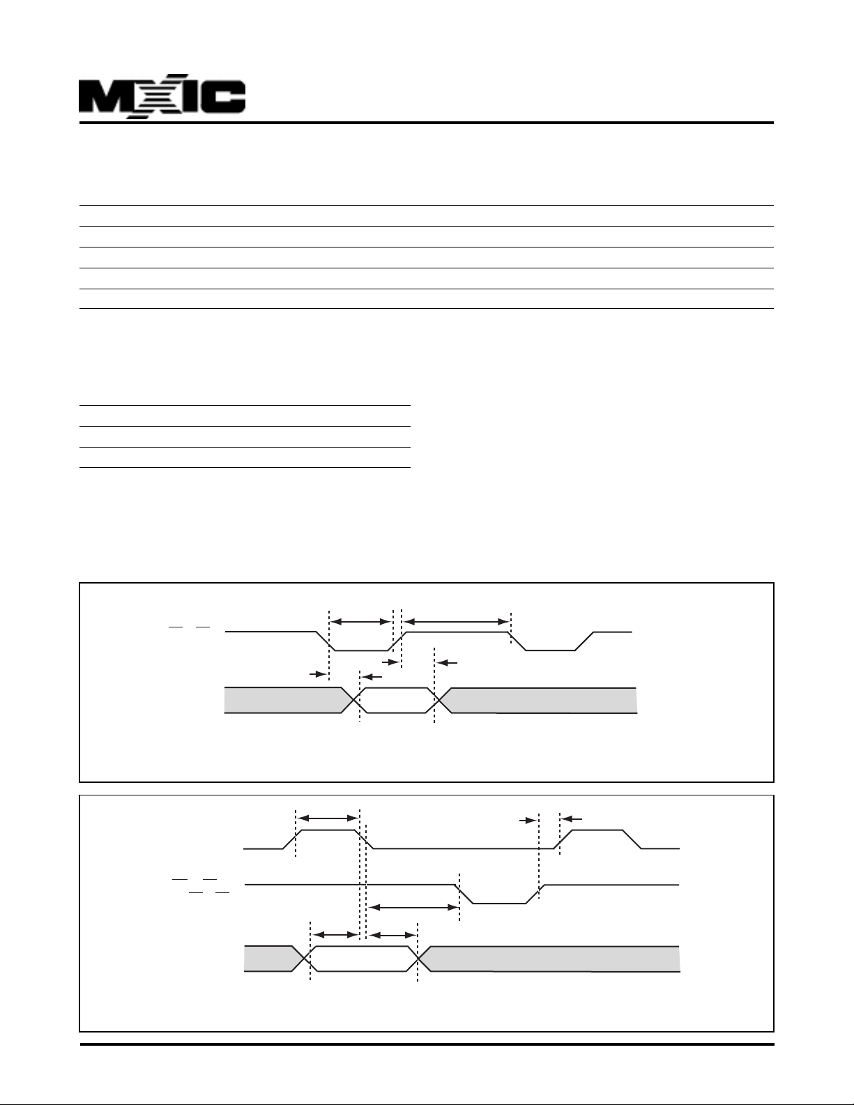
MICROPROCESSOR INTERFACE TIMING----INTERL BUS MODE
tRR
RD x CS
tRD
AD0-AD7
Data
FIGURE 3(a) MICROPRCESSOR READ CYCLE IN INTEL BUS MODE
tRI
tDF
P/N:PM0473
tAD
ALE
WR x CS or
RD x CS
AD0-AD7
tAA
tAL
tALS
tLA
Address
FIGURE 3(b) MICROPROCESSOR WRITE CYCLE IN INTEL BUS MODE
6
REV. 2.5, SEP. 05, 2000
MX97102
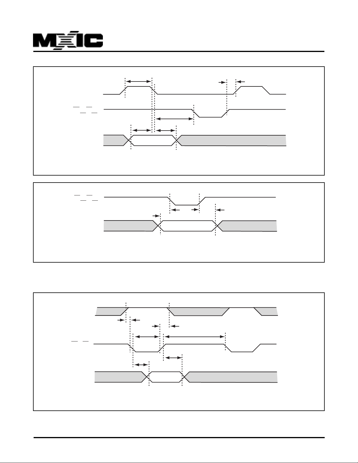
ALE
WR x CS or
RD x CS
AD0-AD7
FIGURE 3(c) MULTIPLEXED ADDRESS TIMING IN INTEL BUS MODE
WR x CS or
RD x CS
A0-A5
tAA
tAL
Address
tAS
tAD
tALS
tLA
tAH
Address
FIGURE 3(d) NON-MULTIPLEXED ADDRESS TIMING IN INTEL BUS MODE
MOTOROLA BUS MODE
ALE
CS x DS
D0-D7
FIGURE 4(a) MICROPROCESSOR READ TIMING IN MOTOROLA BUS MODE
tDSD
tRD
tRR
tRWD
tRI
tDF
Data
P/N:PM0473
REV. 2.5, SEP. 05, 2000
7
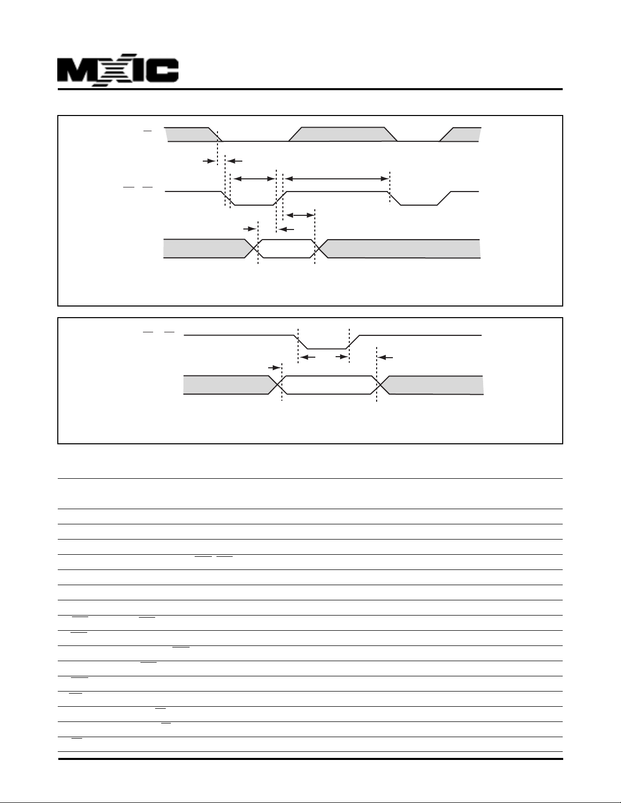
R/W
MX97102
tDSD
CS x DS
D0-D7
tWW
tWD
tDW
Data
tWI
FIGURE 4(b) MICROPROCESSOR WRITE TIMING IN MOTOROLA BUS MODE
CS x DS
AD0-AD5
tAS
Address
tAH
FIGURE 4(c) NON-MULTIPLEXED ADDRESS TIMING IN MOTOROLA BUS MODE
TABLE 6: PARAMETERS FOR MICROPROCESSOR INTERFACE TIMING
P ARAMETER SYMBOL Limit Value UNIT
min. max.
ALE pulse witdh tAA 40 ns
Address setup time to ALE tAL 10 ns
Address hold time to ALE tLA 10 ns
Address latch setup time to WR, RD tALS 0 ns
Address setup time tAS 10 ns
Address hold time tAH 10 ns
ALE guard time tAD 15 ns
DS delay after RW setup tDSD 0 ns
RD pulse width tRR 50 ns
Data ouput delay from RD tRD 50 ns
Data float from RD tDF 52 ns
RD control interval tRI 50 ns
W pulse width tWW 50 ns
Data setup time to W, CS tDW 10 ns
Data hold time from W, CS tWD 10 ns
W control interval tWI 50 ns
P/N:PM0473
8
REV. 2.5, SEP. 05, 2000
Functional and Operational Description
ISDN ACCESS ARCHITECTURE
MX97102
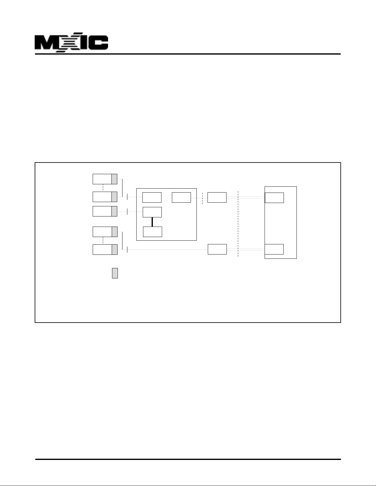
MX97102 is designed especially for subscriber terminal equipment with S/T interfaces, F our wire , tw o pairs
for transmission and receiption separately, are connected to the NT equipment at the user site. Via the NT
equipment, subscribers could dial up to the wide-area
network with the traditional telephone line. The NT
serves a converter between the U interface at the ex-
TE(1)
S
TE(8)
S
TE(1)
TE(1)
S
TE(8)
= MX97102
LT-S LT-T
LT-S
LT-S
Direct Subscriber Access
PBX(NT2)
where - TE is an ISDN terminal
- LT-S is a subscriber line termination
- LT-T is a trunk line termination
- LT is a trunk line termination in the central office
change and the S interface at the user premises. The
NT may be either an NT1 only or an NT1 together with
an NT2 connected via the T interface which is physically identical to the S interface. NT2 may include higher
level functions like multiplexing and switching as in a
PBX. Figure 5 illustrates the connections between the
user site to the public domain of central office.
ISDN
central office
T
NT1
U
telephone
line
LT
LTNT1
FIGURE 5 : ISDN - BASIC SUBSCRIBER ACCESS ACHITECTURE
MX97102 is based on the ISDN basic access, 192kbit/
s, which consists of two circuit-switched 64 kbit/s B
channels and a message oriented 16kbit/s D channel
for packetized data, signaling and telemetry information. The D channel is processed by the LAPD controller contained in the MX97102 and routed via a parallel
CPU interface to the terminal processor. The high level
support of the LAPD protocol which is implemented by
the MX97102 allows the use of a low cost processor in
cost sensitive applications.
P/N:PM0473
REV. 2.5, SEP. 05, 2000
9
GCI CONNECTION
MX97102
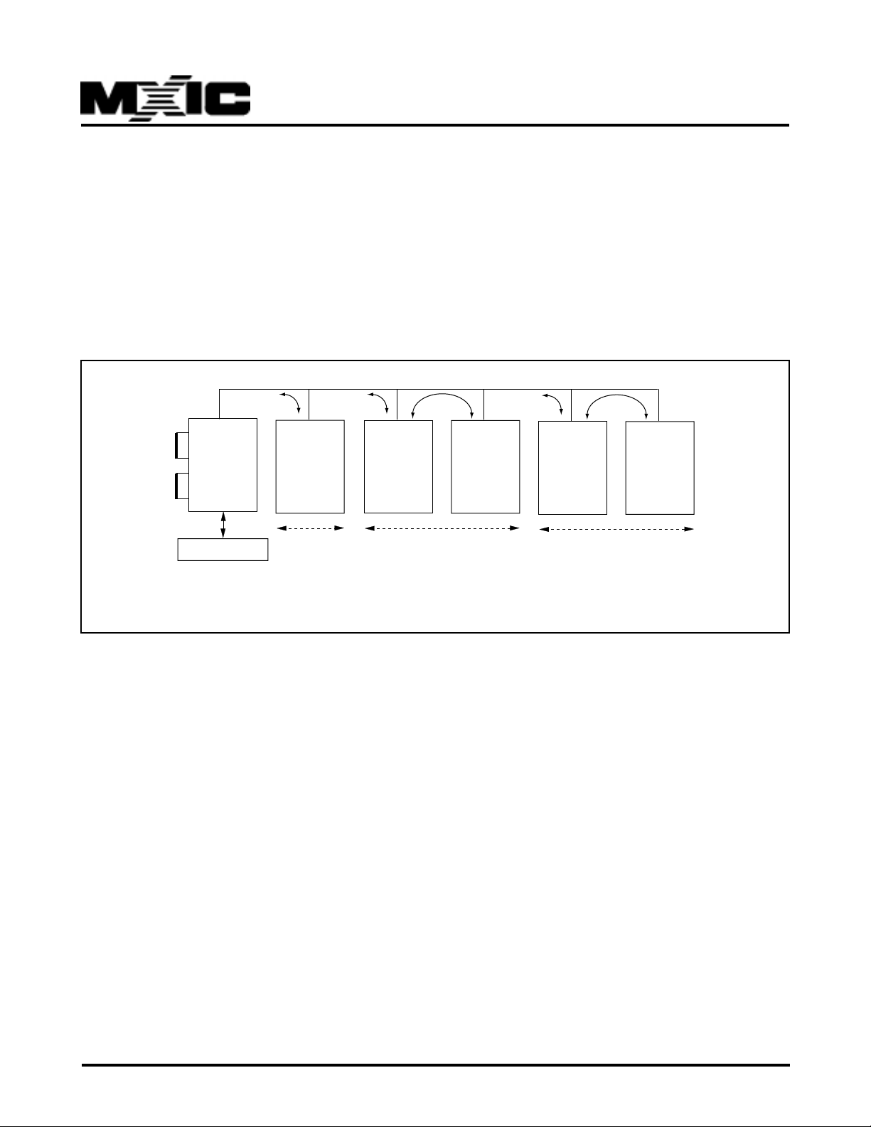
With the GCI interface, MX97102 could connect diff erent voice/data (V/D) application modules. Up to eight
D-channel components may be connected to the D and
C/I (Command/Indication) channels (TIC-bus). TIC-b us
arbitration is also implemented in MX97102.
Data transfers between the MX97102 and the V/D modules are done with the help of the GCI MONITOR channel protocol. Each V/D module can be accessed by an
MX97102
Microprocessor
D, C/I
Data
Module
A
Data
Module
B1
Speech
Processing
Speech Modules
FIGURE 6: EXAMPLES OF GCI CONNECTION
individual address. Two intercommunication channels
IC1 and IC2 allow a 2*64kbit/s transfer rate between
voice/data modules. Figure 6 shows one GCI connection, data module A uses D-channel for data transf er , a
voice processor is connected to a programmable digital processing codec filter via IC1 and a data encryption module to a data device via IC2. Meanwhile, B1 is
used for voice communication, B2 for data communication.
B1
DSP Codec
Module
Data
Encryption
Data Modules
Data
Module
B
GCI FUNCTIONS
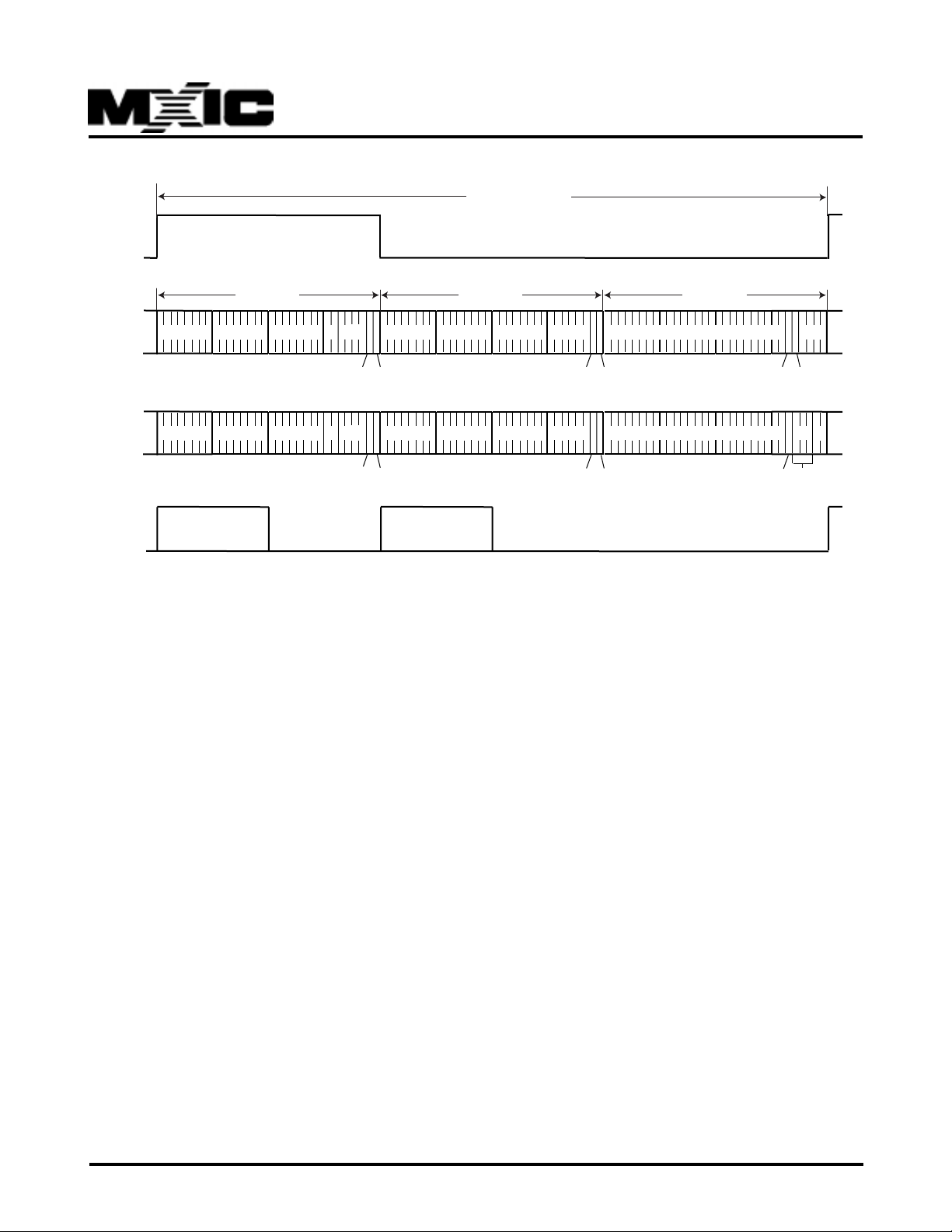
In terminal applications, the GCI constitutes a powerful backplane bus offering intercommunication and sophisticated control capabilities for peripheral modules. GCI frame is composed of three channels ( see Figure 6-1 belo w):
- Channel 0 contains 144kbit/s (for 2B+D) plus MONITOR and command/indication
channels for the layer-1 device.
- Channel 1 contains two 64kbit/s intercommunication channels plus MONITOR and
command/indication channels for other GCI devices.
- Channel 2 is used for GCI-bus arbitration. Only the command/indication are used in channel 2.
P/N:PM0473
10
REV. 2.5, SEP. 05, 2000
FSC1
MX97102
125 us
CH0 CH1 CH2
IPD0
(DD)
IPD1
(DU)
SDS1
B1
B1
IDP0,1:768 kbit/s
DCL :1536 kHz
FSC1 :8 kHz
B2 MONO
B2 MONO D
CIO
D
MR MX
CIO
MR MX
IC1 IC2 MON1 CI1
IC1 IC2 MON1 CI1
BCL :768 kHz bit clock
SDS1 :8kHz programmable data strobe signal for
selecting one or both B/IC channel(s)
Figure 6-1 Frame structure of GCI
The GCI interface is operated in the “open drain” mode
in order to takes advantage of the b us capability. In this
case pull-up resisters (1kohm-5kohm) are required on
PIDP0 and PIDP1.
GCI OFF Function
In GCI terminal mode (SPCR:SPM=0) the GCI interface can be switched off f or external devices via IOF bit
in ADF1 register. If IOF=1, the interface is switched off .
Thus, DCL, FSC1, IDP0/1 and BCL are high impedence.
GCI Direction Control
MR MX S/G
MR MX
A/B
BAC TAD
GCI has the 12-byte frame structure consisting of channels 0, 1 and 2. (see figure 6-1 above)
- IDP0 carries the 2B+D channels from the S/T interface, and the MONITOR 0 and C/I 0 channels coming
from the S/T controller;
- IDP1 carries the MONITOR 0 and C/I 0 channels to
the layer-1.
Channel 1 of GCI interface is used f or internal communication in terminal applications. Two cases have to be
distinguished, according to whether the MX97102 is operated as a master device or as a slave device.
For test applications, the direction of IDP0 (DD) and
IDP1 (DU) can be reversed during certain time-slots
within the GCI frame. This is performed via the IDC bit
in the SQXR register. For normal operation SQXR:IDC
should be set to “0”.
P/N:PM0473
REV. 2.5, SEP. 05, 2000
11
MX97102
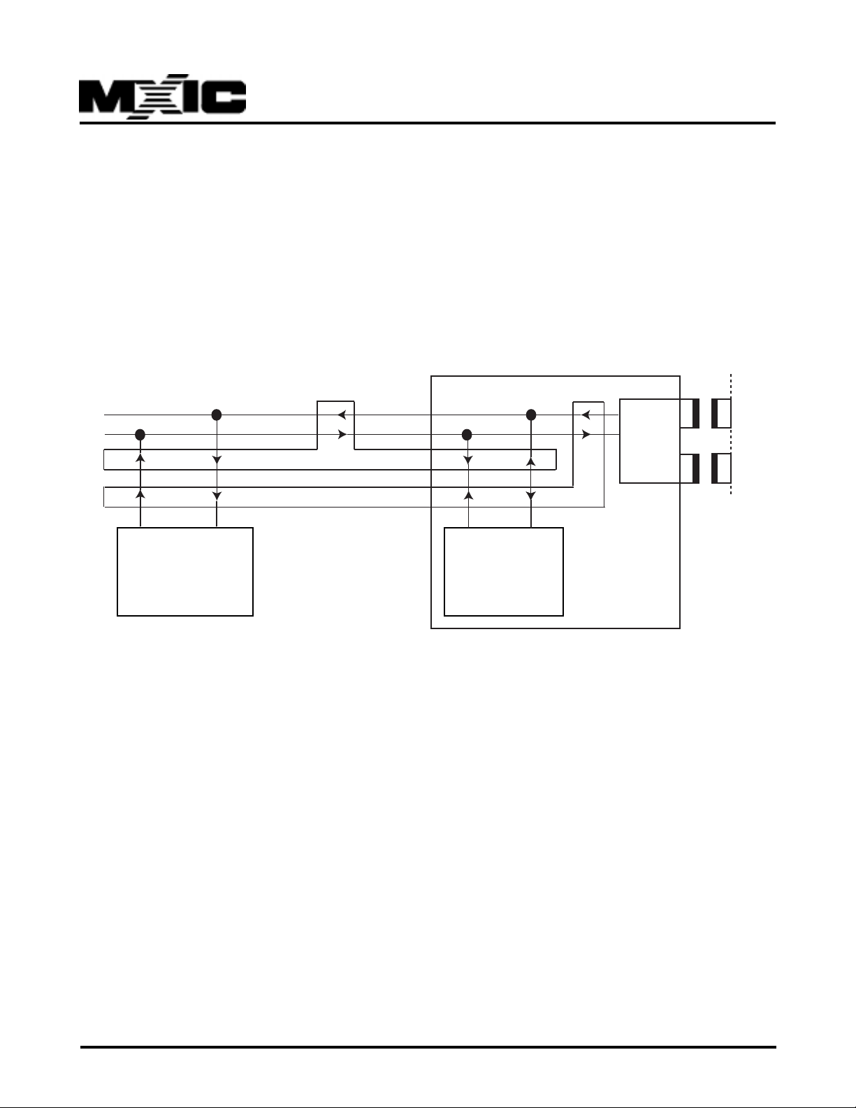
If IDC is set to "0" (master mode):
- IDP0 carries the MONITOR 1 and C/I 1 channels as output to peripheral (voice/data) devices;
- IDP0 also carries the IC channels as output to other devices, if programmed (CxC1-0=01 in register SPCR).
If IDC is set to "1" (slave mode):
- IDP1 carries the MONITOR 1 and C/I 1 channels as output to a master device;
- IDP0 carries the IC channels as output to other devices, if if programmed (CxC1-0=01 in register SPCR).
Figure 6-2shows the connection in a multifunctional terminal with the MX97102 as a master and a Voice/Data
module as a slave device.
S/T interface
GCI interface
DD
DU
IDP0
IDP1
IDP0
IDP1
IDP1
IDP0
MON1, C/I1, IC1, IC2
2B+D, C/I0, S/G, TIC
IDP1
IDP0
Layer1
MX97102
Voice/Data
Module as slave
Layer2
Figure 6-2 GCI port connection and Data direction
If GCI-0 of MODE register is programmed, bit 5 of the last byte in channel 2 on IDP0 can be used to indicate the
S-bus state (stop/go bit) and bit 2 to 5 of the last byte are used for TIC-bus access arbitration.
as Master
P/N:PM0473
REV. 2.5, SEP. 05, 2000
12

Microprocessor Access to B and IC Channels
MX97102
The microprocessor can access the B and IC channels
at the GCI interface by reading the B1CR/B2CR or by
reading and writing the C1R/C2R registers. Furthermore
it is possible to loop back the B channels from/to the S/
Four different functions are selected by the bits CxC1
and CxC0 in the SPCR register. Moreover, each channel, B channel 0/1 and IC channel 0/1, is programmed
individually. Table7-1 shows the configurations.
T interface or to loop back the IC channels from/to the
GCI interface without CPU intervention.
CxC1 CxC0 CxR Read CxR Write BxCR Read Output to GCI Applications
0 0 ICx - Bx - Bx, ICx monitoring
0 1 ICx ICx Bx ICx Bx monitoring, ICx looping
from/to GCI
1 0 - B x Bx Bx Bx access from/to S;
transmission of a constant
value in Bx channel to S
1 1 Bx Bx - Bx Bx looping from S;
transmission of a variable
pattern in Bx channels to S
Table 7-1 CPU access to B/IC channels by SPCR register
Note: x=1 for channel 1 or x=2 for channel 2
If the B-channel access is used for transferring 64kbit/
s voice/data information directly from the CPU port to
the ISDN S/T interface, the access can be synchronized to the GCI interface by means of a synchronous
transfer interrupt programmed in the STCR register.
The general sequence of operations to access the B/
IC channels is:
1. Program synchronous interrupt (ST0) which causes
the device to generate an SIN interrupt at the beginning of an GCI frame.
2. Read or write register (BxCR, CxR)
3. Set SC0 bit in the STCR to acknowledge SIN interrupt.
repeat this sequence from 1 to 3.
Same procedure could be used at ST1 and SC1 bits in
the STCR register. The only difference is ST1 gener-
ates an SIN interrupt at the middle of an GCI frame
instead of at the beginning.
When CPU accesses B channels, we can set the IOF
bit to switch off the GCI function. Thus , external B-chan-
nel sources (voice/data modules) can not disturb the
B-channel access on the GCI interface.
P/N:PM0473
REV. 2.5, SEP. 05, 2000
13
 Loading...