MXIC MX93521 Datasheet

1. FEATURES
MX93521
ALL DIGITAL VOICE RECORDER MACHINE
BASED ON THE MX93521 VOCODER CHIP
• Excellent sound quality by adopting 4800bps CELP
speech compression alogorithm.
• Silent Compression algorithm to further compress si
lence between speech.
• Flash Memory Management alogorithm to manage
down-graded Flash Memory to store compressed
speech data. With silent compression, one 4Mbit flash
memory could store up to 18 minutes speech.
• Support 4/8/16/32 Mbit Samsung Flash Memory or its
compatible parts
• Support both parallel and serial microprocessor inter
face.
• Codec Interface circuit (support both TP3054 and
MX93000)
• Host controllable LCD Module Interface
• Host writable message header (4 bytes) for identifica
-tion or index purpose
• Powerful Editing Function
• Varieties of operating function including Rewind, Fast
Forward, Repeat and message editing etc.
• Voice activated recording
• Use Flash memory to store user data (data bank)
• Upload/Download speech message data from/to
HOST
• VOCODER mode (VOice COmpressor/
DEcompressoR)
• Direct CODEC Play Mode (Play PCM/u-Law data re
ceived from HOST)
• Play Voice Prompt from ROM/FLASH memory
• DTMF tone genarator
2.GENERAL DESCRIPTION
This document describes how to implement an all-digital voice recorder using the MX93521 chip. The MX93521 is a
Digital Recorder Data Pump which is controlled by an external microprocessor to perform various recorder function.
The MX93521 is fully controlled by a HOST controller through a simple HOST interface protocol. The HOST could
initiate many digital recording functions such as record, play, repeat, search, skip, insertion, message managing
and self-diagnosis. Also, HOST could set MX93521 in VOCODER mode and use MX93521 as a speech compression/decompression data pump. The functions supported by MX93521 are listed as followed.
MODE FUNCTION PATH
RECORD CODEC-->(COMPRESS)-->FLASH
PLAY CODEC-->(DECOMPRESS)<--FLASH
RECORD (VOCODER) CODEC-->(COMPRESS)-->HOST
PLA Y (V OCODER) CODEC-->(DECOMPRESS)<--HOST
DIRECT CODEC PLA Y MODE CODEC-->(PCM/u-Law)<--HOST
DOWNLOAD MESSAGE FLASH(MSG)-->HOST
UPLOAD MESSAGE FLASH(MSG)<--HOST
DATABANK ACCESS FLASH(DATA)<-- -->HOST
P/N:PM0426 REV. 2.2, JAN 20, 1998
1
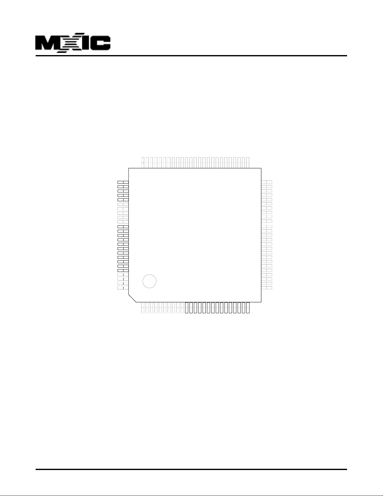
3.PIN CONFIGURATIONS
3.1 Pinout Assignments for MX93521 100-Pin PQFP (Parallel Mode)
100-LQFP PIN ASSIGNMENT¡G
ED8
ED7
ED6
ED5
ED4
ED3
ED2
ED1
GND
VDSP
ED0
HOLD\
HOLDA\
EDCE\
EPCE\
ERD\
EWR\
EAD0
EAD1
EAD2
75747372717069686766656463626160595857565554535251
ED9
ED10
ED11
ED12
ED13
VDSP
GND
ED14
ED15
XTLI
XTLO
NC
NC
NC
NC
MIC-E\
SPK-E\
RST\
EROM
SDEN\
SDATA
WP\
RxCmd
NC
NC
76
77
78
79
80
81
82
83
84
85
86
87
88
89
90
91
92
93
94
95
96
97
98
99
100
MX93521
EAD3
EAD4
EAD5
EAD6
FLL\
MX93521
50
49
48
47
46
45
44
43
42
41
40
39
38
37
36
35
34
33
32
31
30
29
28
27
26
EAD7
NC
EAD8
EAD9
EAD10
EAD11
EAD12
EAD13
EAD14
GND
VDSP
EAD15
VDSP
SCLK
VDSP
DSPDR
DA\
CMCLK
CFS
DSPDX
SOUT
PHDB0
PHDB1
PHDB2
PHDB3
P/N:PM0426
12345678910111213141516171819202122232425
NC
LED2\
LED1\
CE1\
CE2\
NC
ALE
CLE
X32I
X32O
P A CKB\
S/P
SIN
CODEC TYPE
R/B
MTYPE0
SHOLD\
MTYPE2
MTYPE1
GND
VDSP
PHDB7
PHDB6
PHDB5
2
PHDB4
REV. 2.2, JAN 20, 1998
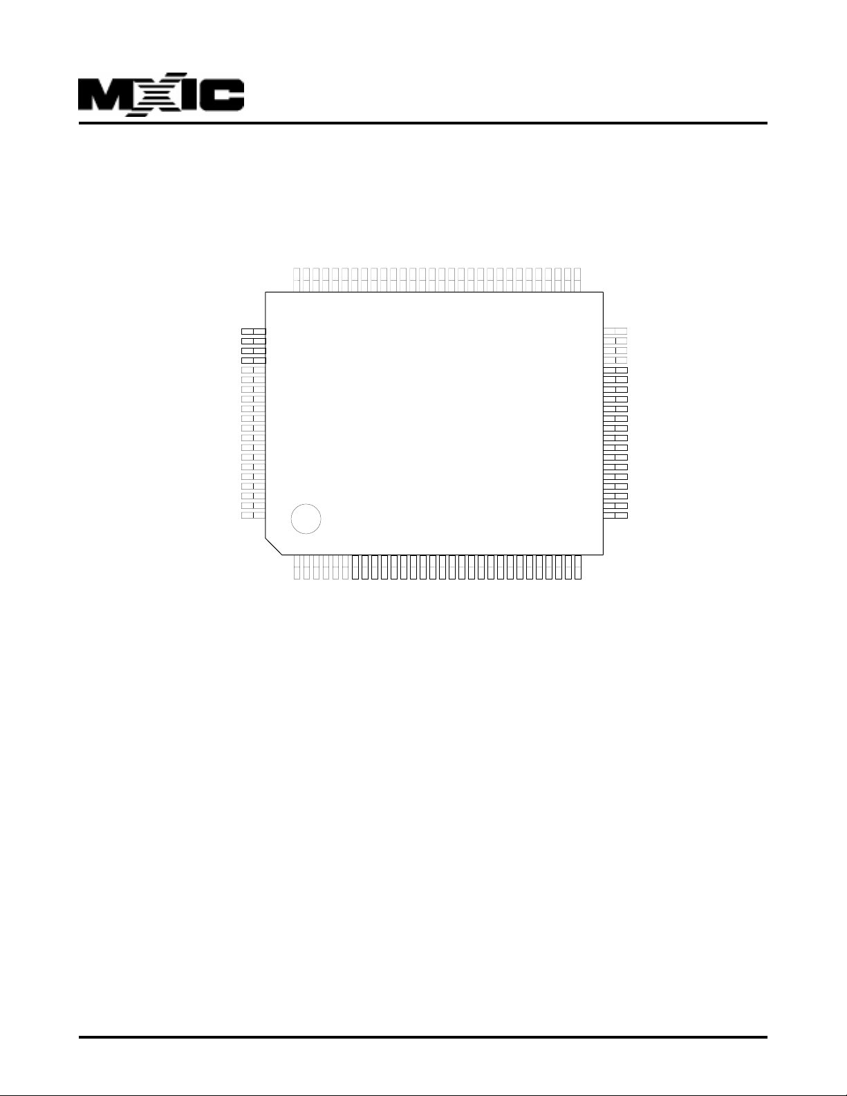
100-PQFP PIN ASSIGNMENT¡G
ED10
ED9
ED8
ED7
ED6
ED5
ED4
ED3
ED2
ED1
GND
VDSP
ED0
HOLD\
HOLDA\
EDCE\
EPCE\
ERD\
EWR\
EAD0
EAD1
EAD2
EAD3
EAD4
EAD5
EAD6
FLL\
GND
EAD7
EAD8
MX93521
ED11
ED12
ED13
VDSP
GND
ED14
ED15
XTLI
XTLO
NC
NC
NC
NC
MIC-E\
SPK-E\
RST\
EROM
SDEN\
SDATA
WP\
8079787776757473727170696867666564636261605958575655545352
81
82
83
84
85
86
87
88
89
90
91
92
93
94
95
96
97
98
99
100
1234567891011121314151617181920212223242526272829
NC
NC
NC
CE1\
CE2\
LED2\
LED1\
RxCmd
NC
ALE
CLE
MX93521
S/P
X32I
X32O
P A CKB\
SIN
R/B
MTYPE0
CODECTYPE
SHOLD\
MTYPE2
MTYPE1
GND
VDSP
PHDB7
PHDB6
PHDB5
PHDB4
51
50
49
48
47
46
45
44
43
42
41
40
39
38
37
36
35
34
33
32
31
30
PHDB3
PHDB2
EAD9
EAD10
EAD11
EAD12
EAD13
EAD14
GND
VDSP
EAD15
VDSP
SCLK
VDSP
DSPDR
PHRDB\
CMCLK
CFS
DSPDX
PHWRB\
PHDB0
PHDB1
P/N:PM0426
REV. 2.2, JAN 20, 1998
3
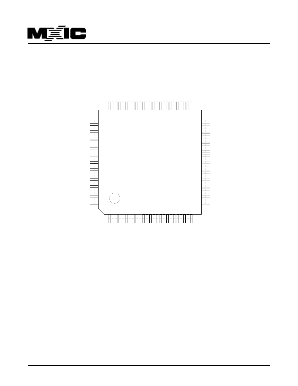
3.2 Pinout Assignments for MX93521 100-Pin TQFP (Serial Mode)
100-LQFP PIN ASSIGNMENT¡G
ED8
ED7
ED6
ED5
ED4
ED3
ED2
ED1
GND
VDSP
ED0
HOLD\
HOLDA\
EDCE\
EPCE\
ERD\
EWR\
EAD0
EAD1
75747372717069686766656463626160595857565554535251
ED9
ED10
ED11
ED12
ED13
VDSP
GND
ED14
ED15
XTLI
XTLO
NC
NC
NC
NC
MIC-E\
SPK-E\
RST\
EROM
SDEN\
SDATA
WP\
RxCmd
NC
NC
76
77
78
79
80
81
82
83
84
85
86
87
88
89
90
91
92
93
94
95
96
97
98
99
100
MX93521
EAD2
EAD3
EAD4
EAD5
EAD6
FLL\
MX93521
50
49
48
47
46
45
44
43
42
41
40
39
38
37
36
35
34
33
32
31
30
29
28
27
26
EAD7
NC
EAD8
EAD9
EAD10
EAD11
EAD12
EAD13
EAD14
GND
VDSP
EAD15
VDSP
SCLK
VDSP
DSPDR
DA\
CMCLK
CFS
DSPDX
SOUT
BIO0
BIO1
BIO2
BIO3
12345678910111213141516171819202122232425
NC
LED2\
LED1\
CE1\
CE2\
NC
ALE
CLE
X32I
X32O
P A CKB\
S/P
SIN
CODEC TYPE
R/B
MTYPE0
SHOLD\
MTYPE2
MTYPE1
GND
VDSP
BIO7
BIO6
BIO5
BIO4
P/N:PM0426
REV. 2.2, JAN 20, 1998
4
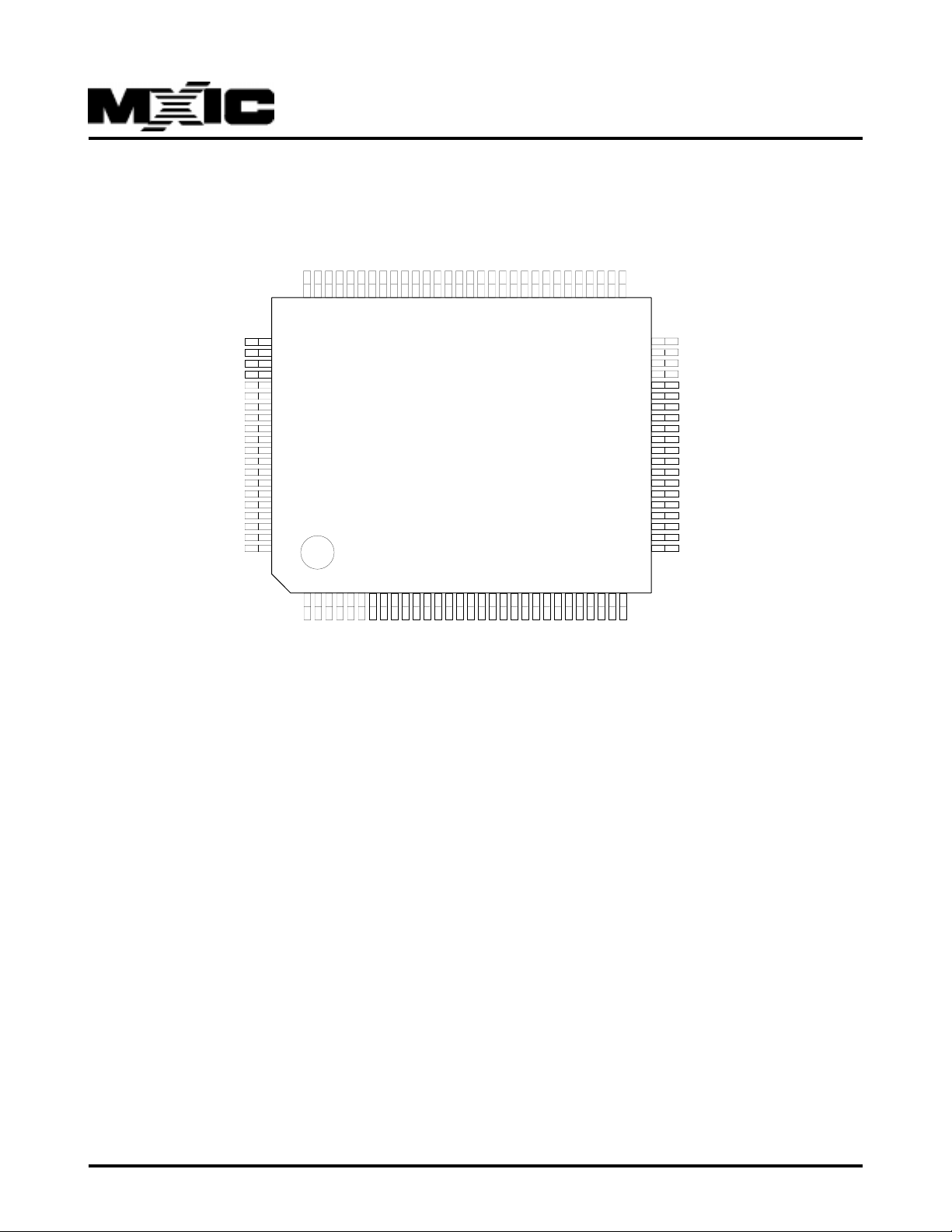
100-PQFP PIN ASSIGNMENT¡G
ED10
ED9
ED8
ED7
ED6
ED5
ED4
ED3
ED2
ED1
GND
VDSP
ED0
HOLD\
HOLDA\
EDCE\
EPCE\
ERD\
EWR\
EAD0
EAD1
EAD2
EAD3
EAD4
EAD5
EAD6
FLL\
GND
EAD7
EAD8
MX93521
ED11
ED12
ED13
VDSP
GND
ED14
ED15
XTLI
XTLO
NC
NC
NC
NC
MIC-E\
SPK-E\
RST\
EROM
SDEN\
SDATA
WP\
8079787776757473727170696867666564636261605958575655545352
81
82
83
84
85
86
87
88
89
90
91
92
93
94
95
96
97
98
99
100
1234567891011121314151617181920212223242526272829
NC
NC
NC
CE1\
CE2\
LED2\
LED1\
RxCmd
NC
ALE
CLE
MX93521
S/P
X32I
X32O
P A CKB\
SIN
R/B
MTYPE0
CODECTYPE
SHOLD\
MTYPE2
MTYPE1
GND
VDSP
BIO7
BIO6
BIO5
BIO4
BIO3
51
50
49
48
47
46
45
44
43
42
41
40
39
38
37
36
35
34
33
32
31
30
BIO2
EAD9
EAD10
EAD11
EAD12
EAD13
EAD14
GND
VDSP
EAD15
VDSP
SCLK
VDSP
DSPDR
PHRDB\
CMCLK
CFS
DSPDX
PHWRB\
BIO0
BIO1
P/N:PM0426
REV. 2.2, JAN 20, 1998
5

MX93521
4.PIN DESCRIPTION
4.1 DSP BASIC (22 PINS )
SYMBOL TYPE PIN # (PQFP) PIN # (LQFP) DESCRIPTION
VDSP 23,43,69,84,41,39 20,40,66,81,38,36 5V power source
GN D 24,44,53,70,85 21,41,67,82 Ground
FLL\ I 54 51 FLL\ low to set MX93521 running from single
low crystal
XTLI 8 8 8 5 32.256Mhz Crystal input
XTLO 89 8 6 32.256Mhz Crystal output
RST\ I 96 9 3 Po wer on Reset, Schmite triggered
PACKB\ OA 1 4 1 1 In serial mode, PACKB\ is N.C.
In parallel mode, PACKB\ becomes low when
MX93521 write data to BIO and high when
HOST read from BIO.
HOLD\ I 67 64 Hold DSP clock down and release bus
HOLDA\ OA 66 63 Ack to HOLD\ signal
EROM I 97 94 Disable internal ROM, use external ROM only
SCLK I 40 37 T ransmit/receive data clock
X32O OA 13 10 32.768Khz Crystal output
X32I 12 9 32.768Khz Crystal input
4.2 DSP EXTERNAL MEMORY(40 pins)
SYMBOL TYPE PIN # (PQFP) PIN # (LQFP) DESCRIPTION
EAD0-EAD15 OB 61~55,52~45,42 58~52,50,48~42,39 Address Bus
ED0~ED15 I/OB 68,71~83,86~87 65,68~80,83~84 Data Bus
EDCE\ OB 6 5 62 External data chip enable
EPCE\ OB 6 4 61 Resered for future use
ERD\ OB 6 3 60 Flash external read
EWR\ OB 6 2 59 Flash external write
NC 90~93 87~90 No connection
4.3 uP INTERF ACE(10 pins)
4.3.1 Serial Interface:(UPMODX=1)
SYMBOL TYPE PIN # (PQFP) PIN # (LQFP) DESCRIPTION
DA \ O C 37 3 4 Data Availab le (Output port OPT17)
SOUT O C 33 30 Serial Data Out (Output port OPT16)
BIO(7..0) OB 25~32 22~29 Drive LCD Display
P/N:PM0426
REV. 2.2, JAN 20, 1998
6

MX93521
4.3.2 Parallel Interface:(UPMODX=0)
SYMBOL TYPE PIN # (PQFP) PIN # (LQFP) DESCRIPTION
PHRDB\ I 3 7 34 Host read
PHWRB\ I 33 30 Host write
PHDB(7:0) B 25~32 22~29 Host data b us
4.4 CODEC (4 pins)
SYMBOL TYPE PIN # (PQFP) PIN # (LQFP) DESCRIPTION
CFS OB 35 3 2 Codec frame sync, 8Khz
CMCLK OB 36 33 Codec master clock, 1.536Mhz
DSPDX OA 34 31 Codec data transmit
DSPDR I 38 35 Codec data receive
4.5 OPT:OUT POR T(16 pins)
SYMBOL TYPE PIN # (PQFP) PIN # (LQFP) DESCRIPTION
CL E OC 1 1 8 Flash memory command latch enable
ALE OC 1 0 7 Flash memory address latch enable
N.C. 6,9 3,6
CE2\ OC 8 5 Chip enable 2
CE1\ OC 7 4 Chip enable 1
LED1\ OC 5 2 LED1 enable
LED2\ OC 4 1 LED2 enable
DR-V5
N.C.
RxCmd
DR-V5
OC 1 98 Received Command (toggle when re
WP\ OC 10 0 97 Flash memory write protection
SD ATA OC 99 96 Serial data transfer (for MX93000)
SDEN\ O C 98 95 Serial data enable (for MX93000)
SPK-E O C 95 92 Speaker enable,Hi-active
MIC-E\ OC 94 91 Microphone enable
2,3
ceived command from HOST)
P/N:PM0426
REV. 2.2, JAN 20, 1998
7

MX93521
4.6 IPT:INPUT POR T(8 pins)
SYMBOL TYPE PIN # (PQFP) PIN # (LQFP) DESCRIPTION
MTYPE1 I 2 2 19 Memory type select 1
MTYPE2 I 2 1 18 Memory type select 2
SHOLD\ I 2 0 17 Power down detect
MTYPE0 I 1 9 16 Memory type select 0
R/B I 1 8 1 5 Flash memory Ready/Busy
CODECTYPE I 1 7 14 Codec select (TP3054B or MX93000)
SIN I 1 6 1 3 Serial data input
S/P\ I 15 1 2 Serial/paralled interface
NOTE:O A:2mA,OB:4mA,OC:16mA output current
P/N:PM0426
REV. 2.2, JAN 20, 1998
8
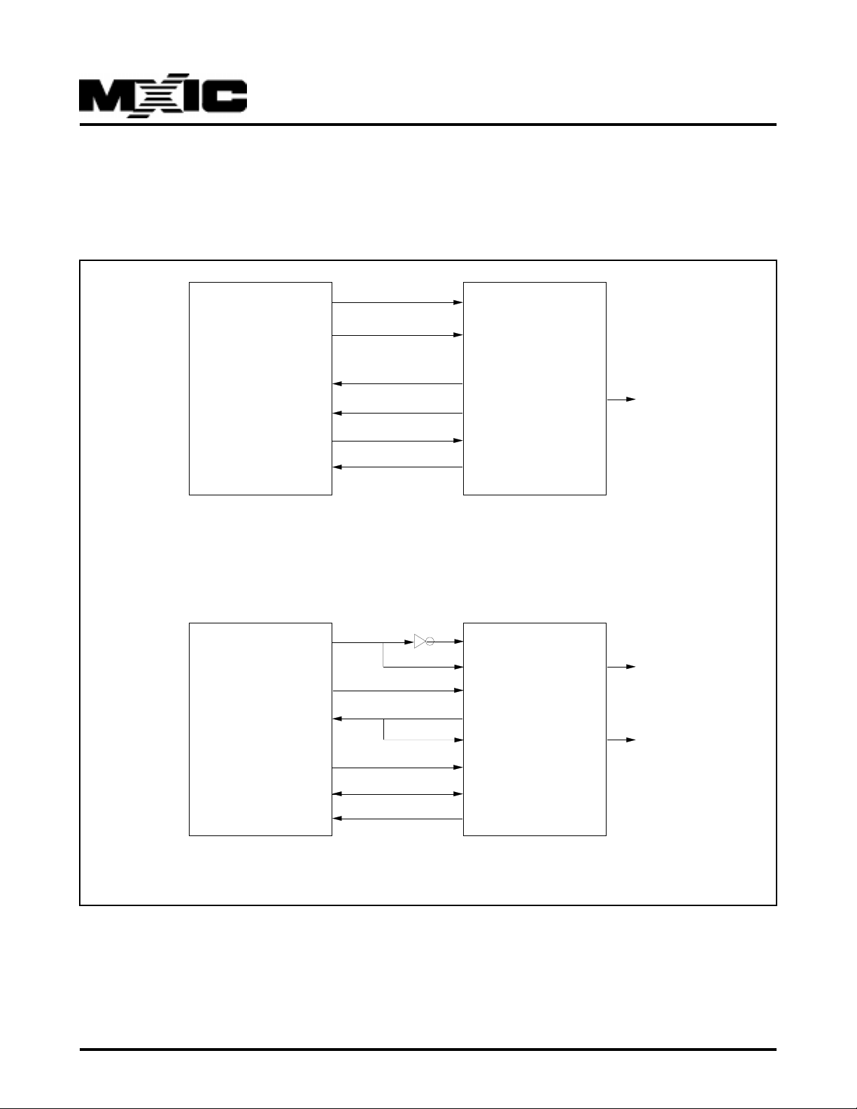
5. HOST CONTROLLER INTERFACE
5.1 HOST CONTROLLER INTERFACE
5.1.1 Configuration
MX93521
HOST
HOST
OUT1
OUT2
IN1
IN2
OUT3
IN3
OUT1
OUT2
IN1
OUT3
D0-7
IN2
40
16
37
33
96
1
SERIAL MODE
33
37
14
16
96
32-25
1
40
SCLK
SIN
DA\
SOUT
RST\
RxCmd
SCLK
PHWRB\
PHRDB\
PACKB\
SIN
RST\
PHDB0-7
RxCmd
MX93521
PHILO\
MX93521
S/P\
S/P\
15
VCC
39
VCC
15
Gnd
P/N:PM0426
PARALLEL MODE
REV. 2.2, JAN 20, 1998
9
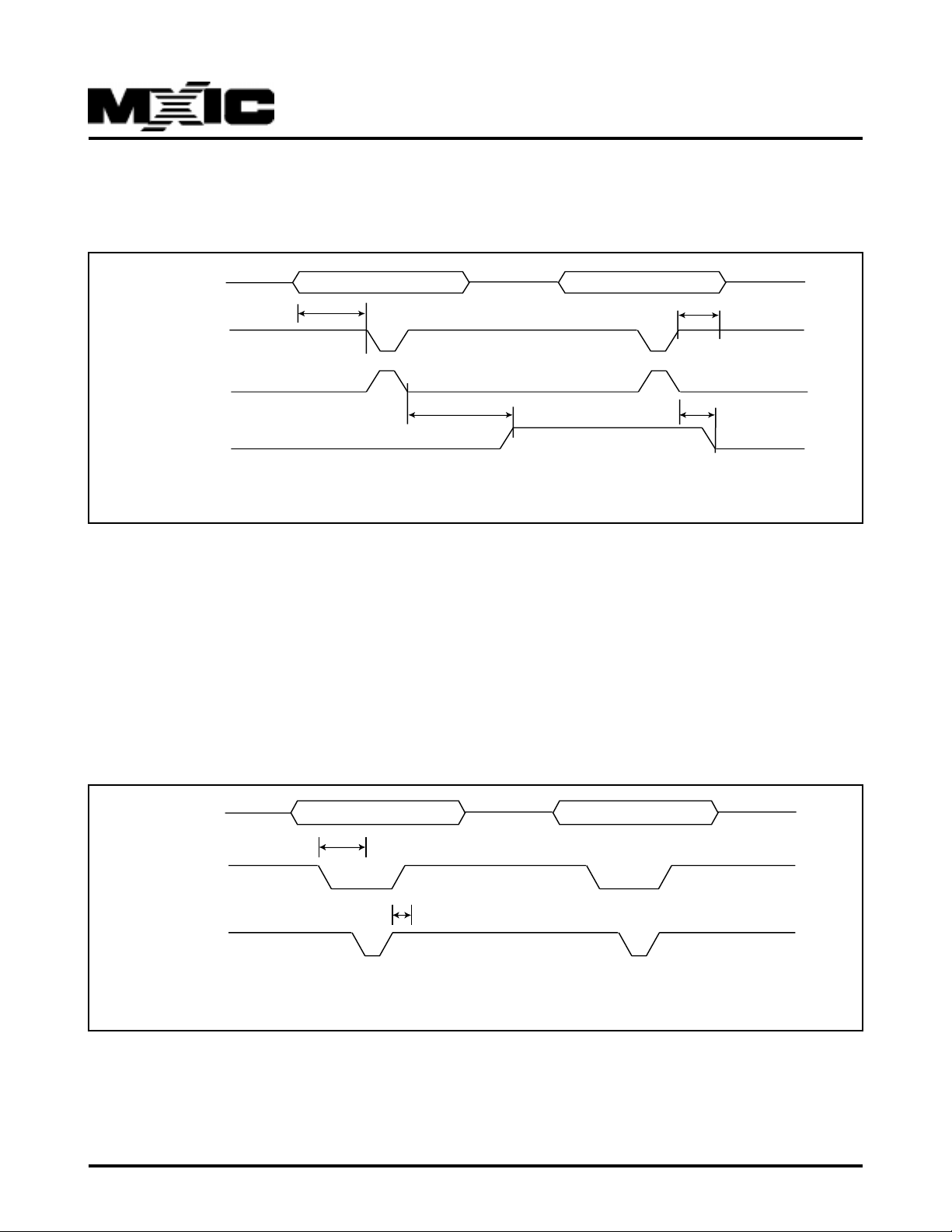
MX93521
5.1.2 Timing Diagrams
HOST Write Timing (Parallel Mode)
PHDB0-7
ts
PHWRB\
SCLK
(INT1\)
RxCmd
HOST Write Timing (Parallel Mode)
tp
HOST should cycle PHWRB\ after writing data to PHDB0-7.
MX93521 will read data from PHDB0-7 on the falling edge of SCLK (rising edge of PHWRB\).
Rxcmd will be toggled if command byte has been processed by MX93521
th
tp
The PHWRB\ signal will cause MX93521 to latch data from bus PHDB0-7 to MX93521 internal register. The invertted
signal of PHWRB\ will trigger MX93521 INT1\ to read and process the received data byte from internal register. Due
to the interrupt contention, there might be an up to 50 us delay between the rising edge of PHWRB\ and INT1\
actually being served. To keep from command overrun, HOST should check if RxCmd toggled or w ait 50 usec before
sending next command byte to MX93521.
HOST Read Timing (Parallel Mode)
PHDB0-7
ts
PACKB\
ta
PHRDB\
HOST Read Timing (Parallel Mode)
When MX93521 write data to PHDB0-7, P ACKB\ will become lo w. HOST needs to poll the status of PACKB\ continuously. When HOST detect low state on PACKB\, HOST should read out data from PHDB0-7. After HOST read the
data from PHDB0-7, PACKB\ will be reset to high.
The maxima delay between MX93521 write data to PHDB0-7 and PACKB\ become low is 10 ns.
The maxima delay between rising edge of PHRDB\ and PACKB\ become high is also 10 ns.
P/N:PM0426
REV. 2.2, JAN 20, 1998
10
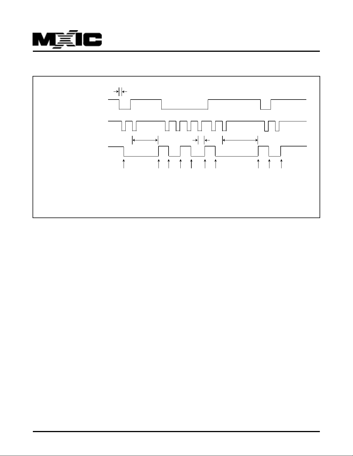
HOST Write Timing (Serial Mode)
HOST output data SIN
HOST output clock SCLK
MX93521
ts
tp
tp
tp
RxCmd
DSP Sampling from SIN
HOST send data 61H tp DSP
start d01d10d20d30d4
0
61H
d5
d61d70stop
1
HOST Write Timing (Serial Mode)
RxCmd become low when start bit is received from HOST and toggle state when MX93521 received each follo wing
data bit or stop bit from HOST . Thus, instead of waiting f or a fixed period of time (50us) to send a command bit, HOST
could send the following command bit as soon as RxCmd toggled from pre vious state. The dela y between the falling
edge of SCLK and the RxCmd togglling time is range from 1 us to 50 us
P/N:PM0426
REV. 2.2, JAN 20, 1998
11
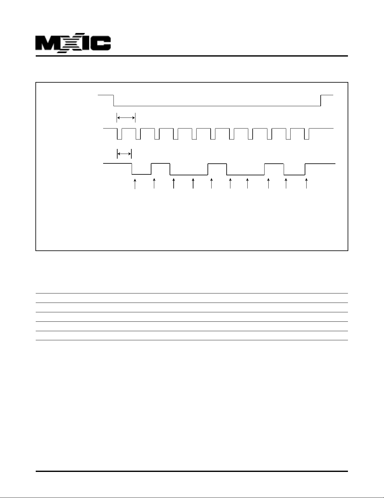
HOST Read Timing (Serial Mode)
DSP inform HOST
Data Available
DA\
>50us, clock rate
HOST output clock
SCLK
5-40us, SOUT response time
DSP output data
SOUT
HOST Sampling from
SOUT
DSP send data 49H
startx
to HOST
d0
d1
1
d2
0
d3
0
1
49H
HOST Read Timing (Serial Mode)
d4
MX93521
d5
0
0
d61d70stop
SOUT response time is 5-40us from the falling edge of SCLK
It is recommended that HOST sample SOUT right before the falling edge of SCLK
uP Interface Timing:
Min Max
Data setup time (ts) 10ns
Data hold time (th) 2ns
Data process time (tp) 1us 50us
PACKB\ acknowledge time (ta) 5ns
P/N:PM0426
REV. 2.2, JAN 20, 1998
12

MX93521
5.2 MX93521 IO INTERF ACE
5.2.1 Output Port
PIN Power do wn state
LED1\ O 5 LED1 CONTROL High
LED2\ O 4 LED2 CONTROL High
UO0* O 3 User Programmable Output Port High
UO1* O 2 User Programmable Output Port High
UO2* O 1 User Programmable Output Port High
* User Programmable Output P ort are only availab le in DR-V3 and DR-V4 v ersion
5.2.2 Flash Memory Interface
MX93521 PIN Flash Power down state
MTYPE1 I 2 2 GN D 0: SAMSUNG
MTYPE2 I 2 1 GN D 0: SAMSUNG
MTYPE0 I 19 Vcc (1:KM29N16000, 0:KM29N040)
CLE O 1 1 CLE Low
ALE O 10 ALE Lo w
ERD\ O 63 RD\
CE2\ O 8 CE2\ High
CE1\ O 7 CE1\ High
EWR\ O 62 WR\
R\B I 18 R/B\
WP\ O 100 WP\ Low
ED0 IO 68 IO0
ED1 IO 71 IO1
ED2 IO 72 IO2
ED3 IO 73 IO3
ED4 IO 74 IO4
ED5 IO 75 IO5
ED6 IO 76 IO6
ED7 IO 77 IO7
5.2.3 CODEC Interface
MX93521 PIN Power down state
CODECTYPE I 1 7 (1: MX93000, 0:TP3054)
DSPDR O 38
DSPDX O 34
CFS O 35
CMCLK O 36
SDA T A O 99 High
SDEN\ O 98 High
SPK_E O 9 5 Lo w
MIC_E\ O 94 High
P/N:PM0426
13
REV. 2.2, JAN 20, 1998

MX93521
5.2.4 uP Serial Mode Interface
MX93521 uP LCD
RxCmd O IN3 (optional) MX93521 Rxd Command Indicator
S/P\ I Vcc High, Serial Mode
SCLK I OUT1 Serial Clock
DA \ O IN1 Data Available
SOUT O IN2 Serial Data Output
SHOLD\ I OUT3 DSP HOLD
SIN I OUT2 Serial Data Input
RST\ I OUT4 DSP RESET
BIO2 O E
BIO3 O RS
BIO4 O D4
BIO5 O D5
BIO6 O D6
BIO7 O D7
5.2.5 uP Parallel Mode Interface
MX93521 uP LCD
S/P\ I GN D Lo w , P ar allel Mode
SCLK I OUT1\
PHRDB\ I OUT2 Read
PHWRB\ I OUT1 Write
SHOLD\ I OUT3 DSP HOLD
RST\ I OUT4 DSP RESET
PHILO\ I Vcc High, Byte Mode
SIN I IN 1 SIN should be connected to PACKB\ externally
PACKB\ O IN1 Acknowledge
RxCmd O IN2 (optional) MX93521 Rxd Command Indicator
PHDB0 I/O D0
PHDB1 I/O D1
PHDB2 I/O D2
PHDB3 I/O D3
PHDB4 I/O D4
PHDB5 I/O D5
PHDB6 I/O D6
PHDB7 I/O D7
When SHOLD\ is low , MX93521 will go to pow er down mode.
When SHOLD\ change from low to high, DSP will power up and send A CK0 to HOST
P/N:PM0426
14
REV. 2.2, JAN 20, 1998

MX93521
6. HOST INTERFACE SOFTWARE COMMAND SET SUMMARY
6.1 HOST TO MX93521 COMMANDS
When MX9521 received a command from HOST, it will always respond the command with a ac knowledge . The
valid commands and corresponded ackno wledge are described as below.
D7 D6 D5 D4 D3 D2 D1 D0
0 0 0 0 1 B B B 008H POINT T O SPECIFIC MESSA GE
0 0 0 1 0 B B B 010H GET CURRENT MESSAGE INFOMATION
0 0 0 1 1 B B B 018H DELETE MESSAGE(S)
0 0 1 0 0 B B B 020H REC/PLAY MISC. FUNCTION
0 0 1 0 1 B B B 028H RECORD MESSAGE
0 0 1 1 0 B B B 030H PLAY MESSAGE
0 0 1 1 1 B B B 038H SKIP FORW ARD/BA CKWARD PLAY
0 1 0 0 0 B B B 040H MISC. FUNCTION
0 1 0 0 1 B B B 048H TONE GENERATOR
0 1 0 1 1 B B B 058H MX93000 CODEC MISC. FUNCTION
0 1 1 0 0 B B B 060H LED DISPLAY
0 1 1 0 1 B B B 068H WRITE COMPRESSED VOICE D A TA TO MX93521
0 1 1 1 0 B B B 070H LCD COMMAND
0 1 1 1 1 B B B 078H LCD D A T A
1 0 0 0 0 B B B 080H OUTPUT COUNTER
1 0 0 0 1 B B B 088H Download/Upload Message
1 0 0 1 0 B B B 090H Set Silence level
DR-V4
1 0 0 1 1 B B B 098H Set ROM/RAM wait state
1 0 1 0 0 B B B 0A0H Read/Write RAM
1 0 1 0 1 B B B 0A8H Read ROM
DR-V4
DR-V5
1 0 1 1 x B B B 0BxH Data Bank Functions
1 1 0 0 x B B B 0CxH Data Bank Functions
1 1 0 1 0 B B B 0D0H Data Bank Functions
1 1 1 1 1 B B B 0F8H Play Voice Prompt
DR-V4
BBB:BYTES SEND FOLLOWING THIS COMMAND
DR-V5
DR-V5
DR-V4
DR-V4
DR-V4
MX93521 T O HOST ACKNO WLEDGES (OK Messages)
ACK0: 0A0H, NO D A TA ACCOMPNIED THIS A CKNOWLEDGE
ACK1: 0A1H, 1 DATA ACCOMPNIED THIS ACKNO WLEDGE
ACK2: 0A2H, 2 DATA ACCOMPNIED THIS ACKNO WLEDGE
ACK6: 0A6H, 6 DATA ACCOMPNIED THIS ACKNO WLEDGE
MX93521 TO HOST A CKNOWLEDGES (ERR OR Messgaes)
ERR0(0E0H): Command ERROR
ERR1(0E1H): Out of memory , MX93521 cannot perform RECORD function
ERR2(0E2H): No message found, MX93521 cannot perform PLA Y function
ERR3(0E3H): No Flash Memory Detected when power on
ERR4(0E4H): MX93521 Busy
ERR5(0E5H): Vocoder Mode , Play b uff er full, data rejected
ERR6(0E6H): No previous or next message found
ERR7(0E7H): MX93000 Command Busy
ERR8(0E8H): No empty block could be allocated for data bank usage
P/N:PM0426
15
DR-V4
REV. 2.2, JAN 20, 1998
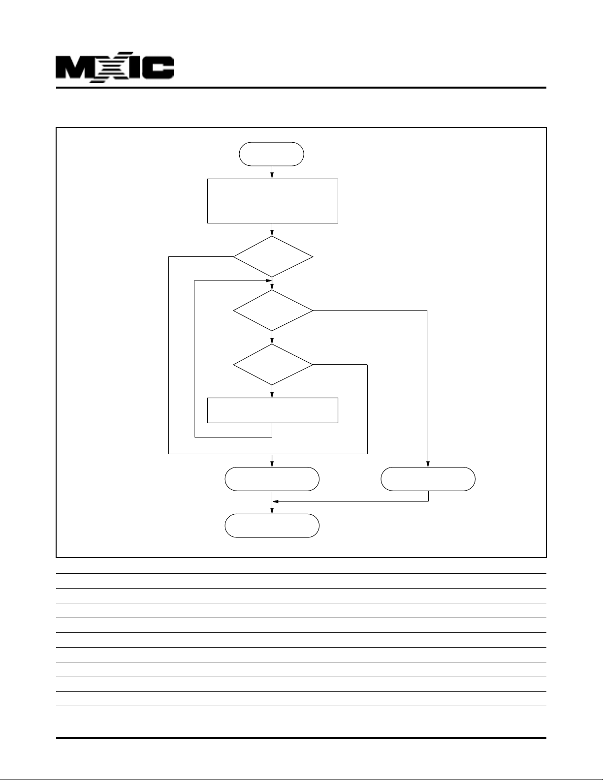
6.2 MX93521 Power On Initialization Flo w Chart
ST ART
Clear MX93521 internal RAM read
systemsetup serial or parallel?
TP3054 or MX93000?
4M or 16M Flash memory init LCD
MX93521
NO
Flash memory
ID correct?
Is data link in
Flash memory correct?
NO
Is check data link
2nd time?
Format Flash memory &
create data link
Flash memory error
send CMD E3H
MX93521 Normal operation
YES
YES
NO
Flash memory OK send CMD
A1H+xxH
0A1H+000H DETECT SAMSUNG KM29N040 FLASH MEMORY
0A1H+001H DETECT SAMSUNG KM29N16000 FLASH MEMORY
0A1H+002H RESERVED
0A1H+003H RESERVED
0A1H+004H RESERVED
0A1H+005H RESERVED
0A1H+006H RESERVED
0A1H+007H RESERVED
ERR3(0E3H) NO MEMORY DETECTED
P/N:PM0426
16
REV. 2.2, JAN 20, 1998

MX93521
6.3 HOST TO MX93521 COMMAND DESCRIPTIONS
COMMAND 09H
FUNCTION: Move Message Pointer
RETURN: ACK0
RETURN: ERR6, IF REACH THE FIRST OR THE LAST MESSA GE IN THE MEMOR Y
DB7 DB6 DB5 DB4 DB3 DB2 DB1 DB0
00001001
DMMMMMMM
IF CURRENT MESSAGE NUMBER IS N,
D=0, JUMP FORW ARD D=1, JUMP BACKW ARD
M=001H, POINT T O THE MESSA GE (N+1) M=001H, POINT T O THE MESSA GE (N-1)
M=002H, POINT T O THE MESSA GE (N+2) M=002H, POINT T O THE MESSA GE (N-2)
M=07FH, POINT T O THE LAST MESSA GE M=07FH, POINT TO THE FIRST MESSA GE
COMMAND 0AH
DR-V5
FUNCTION: P oint to specefic message
RETURN: ACK0
RETURN: ERR2, If no such message found in the FLASH memory
DB7 DB6 DB5 DB4 DB3 DB2 DB1 DB0
00001010
M M M M M M M M Message Number (High Byte)
M M M M M M M M Message Number (Low Byte)
*The message pointer is point to the last message in the flash memory upon power on.
SAMPLES:
Forward to the next message 09 H 0 1H
Rewind to the previous message 09 H 81 H
Forward to the last message 0 9 H 7F H
Rewind to the the first message 09 H F F H
Move Message P ointer to message #258 (102H) 0AH 01 H 02 H
P/N:PM0426
REV. 2.2, JAN 20, 1998
17

MX93521
COMMAND 10H
FUNCTION: GET CURRENT MESSA GE INFOMA TION
RETURN: ACK6, DA TA1, DATA2, DAT A3, D AT A4, D A TA5, D A TA6 or ACK0
DB7 DB6 DB5 DB4 DB3 DB2 DB1 DB0
0001000 0
D ATA1: HIGH BYTE OF CURRENT MESSAGE NUMBER
D ATA2: LOW BYTE OF CURRENT MESSAGE NUMBER
DATA 3: USER DA TA #1
DATA 4: USER DA TA #2
DATA 5: USER DA TA #3
DATA 6: USER DA TA #4
*RETURN ACK0 WHEN NO MESSAGE IN THE MEMOR Y
SAMPLES:
GET CURRENT MESSAGE INFOMATION 10 H
COMMAND 11H
COMMAND 12H
COMMAND 13H
COMMAND 14H
FUNCTION: ATT ACH USER DA T A TO CURRENT MESSAGE
RETURN: ACK0 or ERR0
DB7 DB6 DB5 DB4 DB3 DB2 DB1 DB0
00010BB B
USER DAT A #1
USER DAT A #2
USER DAT A #3
USER DAT A #4
* The USER D ATA is default to 0FFH
* Any data writen with this command will be AND with previous data
* When USER D ATA #1 is 055H. If write data 0AAH to it again, USER D ATA #1 will become 0H
* If no message in the FLASH memory , MX93521 will return ERR0
SAMPLES:
A TTACH D A TA 12H TO CURRENT MESSA GE 11 H 12H
A TTACH D A TA 12H/34H TO CURRENT MESSA GE 12 H 12H 34H
A TTACH D A TA 12H/34H/56H T O CURRENT MESSAGE 1 3H 12H 34H 56 H
A TTACH D A TA 12H/34H/56H/78H TO CURRENT MESSA GE 14 H 12H 34H 56H 78H
P/N:PM0426
REV. 2.2, JAN 20, 1998
18
 Loading...