

MXIC MX29LV64xM H-L Technical data

FEATURES
MX29LV64xM H/L
64M-BIT SINGLE VOLTAGE 3V ONLY
UNIFORM SECTOR FLASH MEMORY
GENERAL FEA TURES
• Single Po wer Supply Operatio n
- 2.7 to 3.6 volt for read, erase, and program operations
• Configuration
- 8,388,608 x 8 / 4,194,304 x 16 switchable (for
MX29L V640M H/L)
- 4,194,304 x 16 (fo r MX29L V641M H/L)
• Sector structure
- 64KB(32KW) x 128
• Sector Protection/Chip Unprotect
- Provides sector group protect function to prevent
program or erase operation in the protected sector
group
- Provides chip unprotect function to allow code
changes
- Provides temporary sector group unprotect function
for code changes in previously protected sector groups
• Secured Silicon Sector
- Pro vides a 128-wo rd/256-byte area f o r co de o r data
that can be permanently protected.
- Once this sector is protected, it is prohibited to program or erase within the sector again.
• Latch-up protected to 250mA from -1V to Vcc + 1V
• Low Vcc write inhibit is equal to o r less than 1.5V
• Compatible with JEDEC standard
- Pin-out and software compatible to single power supply Flash
PERFORMANCE
• High Perf ormance
- Fast access time: 90ns
- Page read time: 25ns
- Sector erase time: 0.5s (typ.)
- 4 word/8 b yte page read buffer
- 16 word/ 32 b yte write buffer: reduces pro gramming
time fo r multiple-wo rd/byte updates
• Low Pow er Consumptio n
- Active read current: 18mA(typ.)
- Active write current: 20mA(typ.)
- Standby current: 20uA(typ.)
• Minimum 100,000 erase/program cycle
• 20-years data retention
SOFTW ARE FEA TURES
• Support Commo n Flash Interf ace (CFI)
- Flash device parameters stored on the device and
provide the host system to access.
• Program Suspend/Pro gram Resume
- Suspend progr am operatio n to read o ther sectors
• Erase Suspend/ Erase Resume
- Suspends sector erase operatio n to read data/program o ther sectors
• Status Reply
- Data# polling & Toggle bits pro vide detectio n o f program and erase operation completion
HARDW ARE FEA TURES
• Ready/Busy (RY/BY#) Output (fo r MX29LV640M H/L
only)
- Provides a hardware method of detecting program
and erase operation completion
• Hardware Reset (RESET#) Input
- Provides a hardware method to reset the internal
state machine to read mode
• WP#/ACC input
- Write protect (WP#) functio n allows pro tectio n highest or lowest sector, regardless of sector protection
settings
- ACC (high voltage) accelerates programming time
for higher throughput during system
P A CKAGE
• 48-pin TSOP (for MX29L V641M H/L)
• 56-pin TSOP (for MX29L V640M H/L)
GENERAL DESCRIPTION
The MX29LV64xM H/L is a 64-mega bit Flash memo ry
organized as 8M bytes of 8 bits or 4M words of 16 bits
(for MX29LV640M H/L), or 4M words of 16bits (for
MX29LV641M H/L). MXIC's Flash memories offer the
most cost-effective and reliable read/write non-volatile
rando m access memory . The MX29L V64xM H/L is packaged in 48-pin TSOP and 56-pin TSOP. It is designed to
P/N:PM1093 REV. 1.1, AUG. 11, 2005
be reprog rammed and er ased in system or in standard
EPROM pro grammers.
The standard MX29LV64xM H/L offers access time as
fast as 90ns, allowing operation of high-speed microprocessors without wait states. To eliminate bus contention, the MX29LV64xM H/L has separate chip enable
1

MX29LV64xM H/L
(CE#) and o utput enable (OE#) co ntrols .
MXIC's Flash memories augment EPROM functionality
with in-circuit electrical erasure and prog ramming. The
MX29L V64xM H/L uses a co mmand register to manage
this functionality.
MXIC Flash technology reliably stores memory contents
even after 100,000 er ase and program cycles. The MXIC
cell is designed to optimize the erase and program
mechanisms. In addition, the combination of advanced
tunnel oxide processing and low internal electric fields
for erase and programming operations produces reliable
cycling. The MX29LV64xM H/L uses a 2.7V to 3.6V
VCC supply to perform the High Reliability Erase and
auto Progr am/Erase algorithms.
The highest degree of latch-up protection is achieved
with MXIC's proprietary non-epi process. Latch-up protection is proved for stresses up to 100 milliamperes on
address and data pin from -1V to VCC + 1V.
AUTOMATIC PROGRAMMING
The MX29L V64xM H/L is byte/wo rd/page pro grammable
using the Auto matic Pro gramming algo rithm. The Automatic Programming algorithm makes the external system do not need to ha ve time o ut sequence no r to verify
the data prog rammed.
AUTOMATIC PROGRAMMING ALGORITHM
MXIC's Automatic Programming algorithm require the user
to only write program set-up commands (including 2 unlock write cycle and A0H) and a program command (program data and address). The de vice automatically times
the programming pulse width, provides the program verification, and counts the number of sequences. A status
bit similar to DATA# polling and a status bit to ggling between consecutive read cycles, provide feedback to the
user as to the status of the programming operation.
AUTOMATIC CHIP ERASE
The entire chip is bulk erased using 50 ms erase pulses
according to MXIC's A utomatic Chip Er ase algorithm. The
Automatic Erase algorithm automatically programs the
entire array prio r to electrical erase. The timing and veri-
fication o f electrical erase are co ntro lled internally within
the device.
AUTOMATIC SECTOR ERASE
The MX29L V64xM H/L is secto r(s) erasable using MXIC's
Auto Secto r Erase algo rithm. Secto r erase mo des allo w
sectors o f the arra y to be erased in o ne erase cycle. The
Auto matic Sector Er ase algorithm auto matically progr ams
the specified sector(s) prio r to electrical erase. The timing and verificatio n of electrical erase are co ntrolled internally within the device.
AUTOMATIC ERASE ALGORITHM
MXIC's Automatic Erase algorithm requires the user to
write commands to the command register using standard micropro cesso r write timings. The de vice will automatically pre-prog r am and verify the entire array. Then
the device automatically times the erase pulse width,
provides the erase verification, and counts the number
of sequences. A status bit toggling between consecutive read cycles provides feedback to the user as to the
status of the programming operation.
Register contents serve as inputs to an internal statemachine which controls the erase and programming circuitry . During write cycles, the co mmand register internally latches address and data needed for the programming and erase operations. During a system write cycle,
addresses are latched on the falling edge, and data are
latched on the rising edge o f WE# .
MXIC's Flash technology combines years of EPROM
experience to pro duce the highest le vels of quality, reliability, and cost effectiveness. The MX29LV64xM H/L
electrically erases all bits simultaneously using FowlerNordheim tunneling. The bytes are pro grammed b y using the EPROM programming mechanism of hot electron injection.
During a program cycle, the state-machine will control
the program sequences and command register will not
respond to any command set. During a Sector Erase
cycle, the command register will only respond to Erase
Suspend command. After Erase Suspend is completed,
the device stays in read mode. After the state machine
has completed its task, it will allow the command register to respond to its full command set.
P/N:PM1093
REV. 1.1, AUG. 11, 2005
2
PIN CONFIGURATION
48 TSOP f or MX29LV641M H/L
MX29LV64xM H/L
A15
A14
A13
A12
A11
A10
A21
A20
WE#
RESET#
ACC
WP#
A19
A18
A17
1
2
3
4
5
6
7
A9
8
A8
9
10
11
12
13
14
15
16
17
18
A7
19
A6
20
A5
21
A4
22
A3
23
A2
24
A1
56 TSOP for MX29L V640M H/L
MX29LV641M H/L
(Normal T ype)
A16
48
VI/O
47
VSS
46
Q15
45
Q7
44
Q14
43
Q6
42
Q13
41
Q5
40
Q12
39
Q4
38
V
37
36
35
34
33
32
31
30
29
28
27
26
25
CC
Q11
Q3
Q10
Q2
Q9
Q1
Q8
Q0
OE#
VSS
CE#
A0
NC
NC
A15
A14
A13
A12
A11
A10
A19
A20
WE#
RESET#
A21
WP#/ACC
RY/BY#
A18
A17
NC
NC
1
2
3
4
5
6
7
8
9
A9
10
A8
11
12
13
14
15
16
17
18
19
20
A7
21
A6
22
A5
23
A4
24
A3
25
A2
26
A1
27
28
MX29LV640M H/L
(Normal T ype)
NC
56
NC
55
A16
54
BYTE#
53
VSS
52
Q15/A-1
51
Q7
50
Q14
49
Q6
48
Q13
47
Q5
46
Q12
45
Q4
44
V
43
42
41
40
39
38
37
36
35
34
33
32
31
30
29
CC
Q11
Q3
Q10
Q2
Q9
Q1
Q8
Q0
OE#
VSS
CE#
A0
NC
VIO
P/N:PM1093
REV. 1.1, AUG. 11, 2005
3
MX29LV64xM H/L
PIN DESCRIPTION
SYMBOL PIN NAME
A0~A21 Address Input
Q0~Q14 Data Inputs/Outputs
Q15/A-1 Q15(Word Mode)/LSB addr(Byte Mode)
CE# Chip Enable Input
WE# Write Enable Input
OE# Output Enable Input
RESET# Hardware Reset Pin, Active Low
WP#/ACC Hardware Write Protect/Prog ramming
Acceleration input
RY/BY# Read/Busy Output
BYTE# Selects 8 bit or 16 bit mode
VC C +3.0V single power supply
VI/O Output Buffer P ower
GN D Device Ground
N C Pin Not Connected Internally
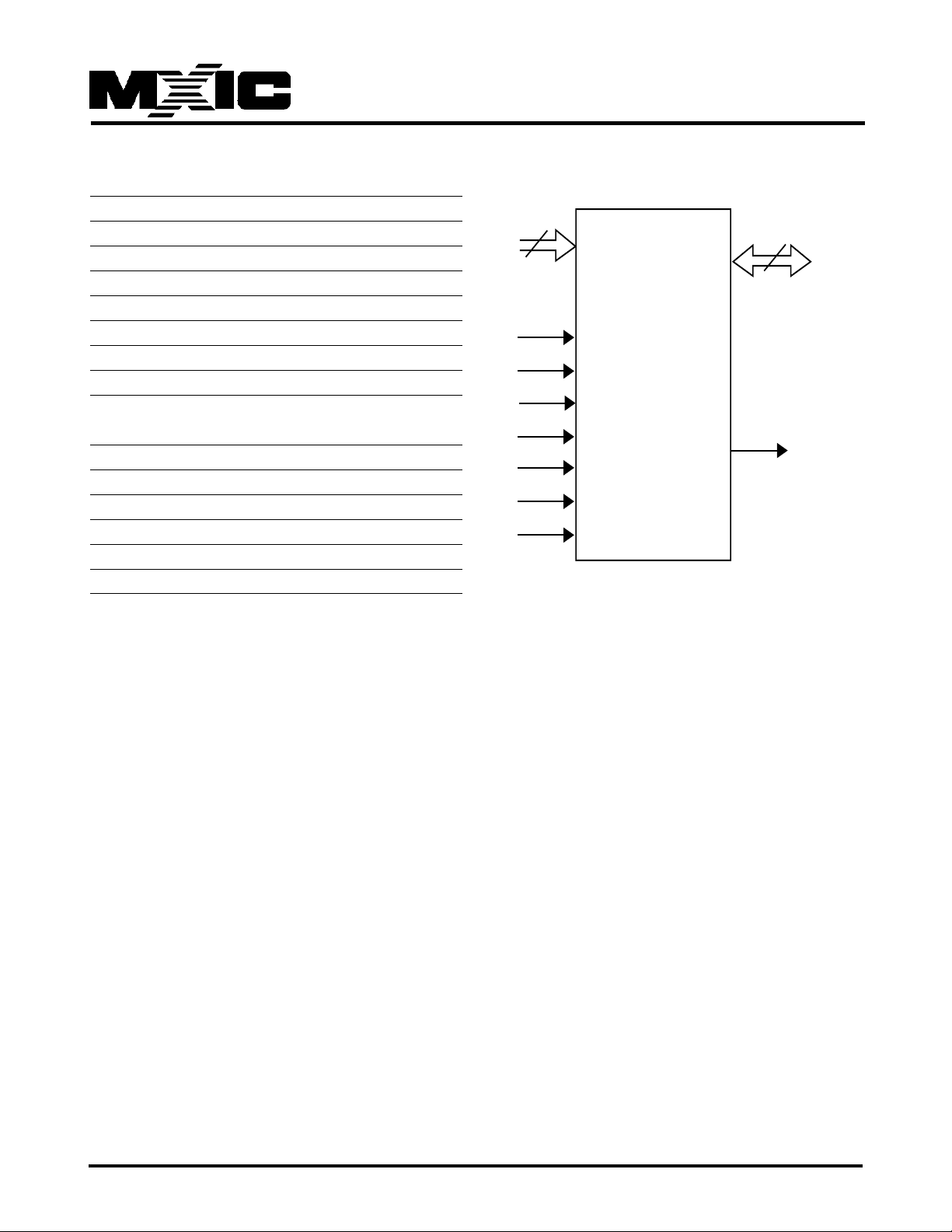
LOGIC SYMBOL
22
A0-A21
CE#
OE#
WE#
RESET#
WP#/ACC
BYTE#
VI/O
Q0-Q15
16 or 8
(A-1)
RY/BY#
P/N:PM1093
REV. 1.1, AUG. 11, 2005
4
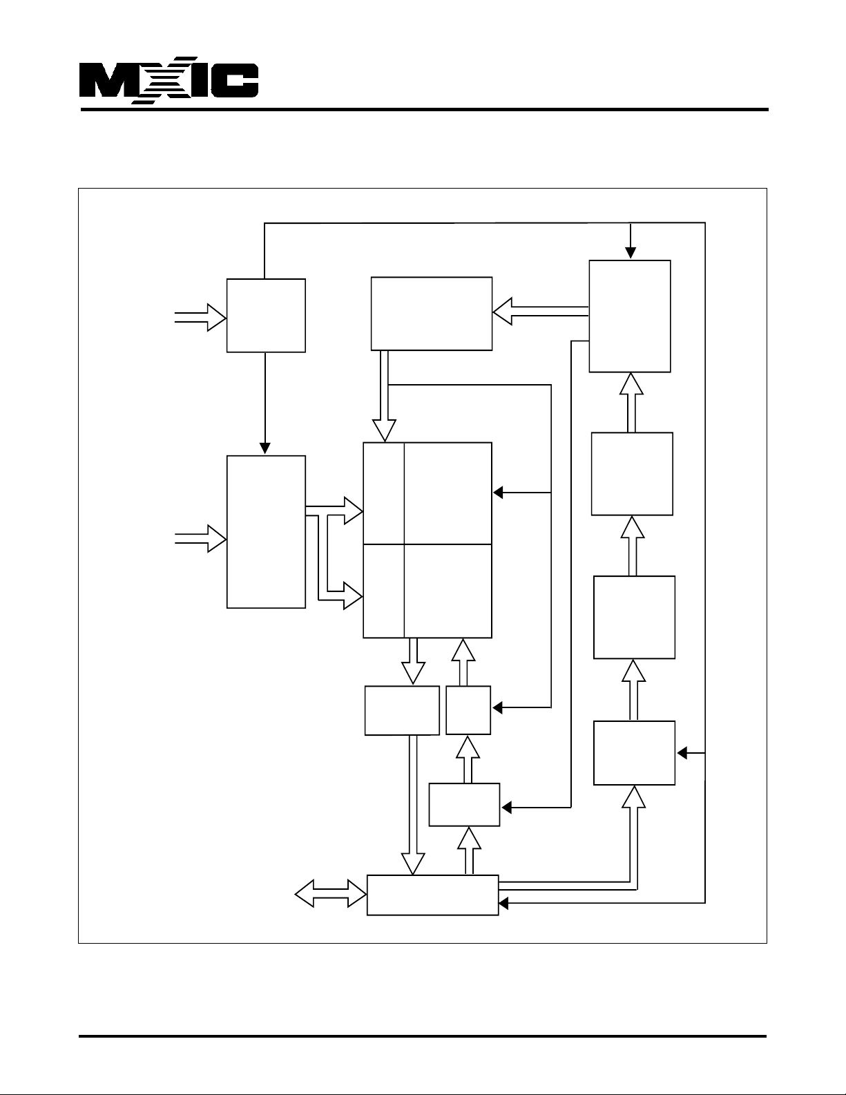
BLOCK DIAGRAM
MX29LV64xM H/L
CE#
OE#
WE#
WP#
BYTE#
RESET#
A0-A21
CONTROL
INPUT
LOGIC
ADDRESS
LATCH
AND
BUFFER
PROGRAM/ERASE
HIGH VOLTAGE
X-DECODER
FLASH
ARRAY
Y-DECODER
Y-PASS GATE
WRITE
STATE
MACHINE
(WSM)
STATE
REGISTER
ARRAY
SOURCE
HV
COMMAND
DATA
DECODER
P/N:PM1093
Q0-Q15
SENSE
AMPLIFIER
DATA LATCH
I/O BUFFER
5
PGM
DATA
HV
COMMAND
DATA LATCH
PROGRAM
REV. 1.1, AUG. 11, 2005
MX29LV64xM H/L
MX29LV64xM H/L SECTOR ADDRESS TABLE
Sector Sector Address Sector Size (x8) (x16)
A21-A12 (Kbytes/Kwords) Address Range Address Range
SA0 0000000xxx 64/32 000000h-00FFFFh 000000h-07FFFh
SA1 0000001xxx 64/32 010000h-01FFFFh 008000h-0FFFFh
SA2 0000010xxx 64/32 020000h-02FFFFh 010000h-17FFFh
SA3 0000011xxx 64/32 030000h-03FFFFh 018000h-01FFFFh
SA4 0000100xxx 64/32 040000h-04FFFFh 020000h-027FFFh
SA5 0000101xxx 64/32 050000h-05FFFFh 028000h-02FFFFh
SA6 0000110xxx 64/32 060000h-06FFFFh 030000h-037FFFh
SA7 0000111xxx 64/32 070000h-07FFFFh 038000h-03FFFFh
SA8 0001000xxx 64/32 080000h-08FFFFh 040000h-047FFFh
SA9 0001001xxx 64/32 090000h-09FFFFh 048000h-04FFFFh
SA10 0001010xxx 64/32 0A0000h-0AFFFFh 050000h-057FFFh
SA11 0001011xxx 64/32 0B0000h-0BFFFFh 058000h-05FFFFh
SA12 0001100xxx 64/32 0C0000h-0CFFFFh 060000h-067FFFh
SA13 0001101xxx 64/32 0D0000h-0DFFFFh 068000h-06FFFFh
SA14 0001110xxx 64/32 0E0000h-0EFFFFh 070000h-077FFFh
SA15 0001111xxx 64/32 0F0000h-0FFFFFh 078000h-07FFFFh
SA16 0010000xxx 64/32 100000h-10FFFFh 080000h-087FFFh
SA17 0010001xxx 64/32 110000h-11FFFFh 088000h-08FFFFh
SA18 0010010xxx 64/32 120000h-12FFFFh 090000h-097FFFh
SA19 0010011xxx 64/32 130000h-13FFFFh 098000h-09FFFFh
SA20 0010100xxx 64/32 140000h-14FFFFh 0A0000h-0A7FFFh
SA21 0010101xxx 64/32 150000h-15FFFFh 0A8000h-0AFFFFh
SA22 0010110xxx 64/32 160000h-16FFFFh 0B0000h-0B7FFFh
SA23 0010111xxx 64/32 170000h-17FFFFh 0B8000h-0BFFFFh
SA24 0011000xxx 64/32 180000h-18FFFFh 0C0000h-0C7FFFh
SA25 0011001xxx 64/32 190000h-19FFFFh 0C8000h-0CFFFFh
SA26 0011010xxx 64/32 1A0000h-1AFFFFh 0D0000h-0D7FFFh
SA27 0011011xxx 64/32 1B0000h-1BFFFFh 0D8000h-0DFFFFh
SA28 0011100xxx 64/32 1C0000h-1CFFFFh 0E0000h-0E7FFFh
SA29 0011101xxx 64/32 1D0000h-1DFFFFh 0E8000h-0EFFFFh
SA30 0011110xxx 64/32 1E0000h-1EFFFFh 0F0000h-0F7FFFh
SA31 0011111xxx 64/32 1F0000h-1FFFFFh 0F8000h-0FFFFFh
SA32 0100000xxx 64/32 200000h-20FFFFh 100000h-107FFFh
SA33 0100001xxx 64/32 210000h-21FFFFh 108000h-10FFFFh
SA34 0100010xxx 64/32 220000h-22FFFFh 110000h-117FFFh
SA35 0100011xxx 64/32 230000h-23FFFFh 118000h-11FFFFh
SA36 0100100xxx 64/32 240000h-24FFFFh 120000h-127FFFh
SA37 0100101xxx 64/32 250000h-25FFFFh 128000h-12FFFFh
SA38 0100110xxx 64/32 260000h-26FFFFh 130000h-137FFFh
SA39 0100111xxx 64/32 270000h-27FFFFh 138000h-13FFFFh
P/N:PM1093
REV. 1.1, AUG. 11, 2005
6
MX29LV64xM H/L
Sector Sector Address Sector Size (x8) (x16)
A21-A12 (Kbytes/Kwords) Address Range Address Range
SA40 0101000xxx 64/32 280000h-28FFFFh 140000h-147FFFh
SA41 0101001xxx 64/32 290000h-29FFFFh 148000h-14FFFFh
SA42 0101010xxx 64/32 2A0000h-2AFFFFh 150000h-157FFFh
SA43 0101011xxx 64/32 2B0000h-2BFFFFh 158000h-15FFFFh
SA44 0101100xxx 64/32 2C0000h-2CFFFFh 160000h-147FFFh
SA45 0101101xxx 64/32 2D0000h-2DFFFFh 168000h-14FFFFh
SA46 0101110xxx 64/32 2E0000h-2EFFFFh 170000h-177FFFh
SA47 0101111xxx 64/32 2F0000h-2FFFFFh 178000h-17FFFFh
SA48 0110000xxx 64/32 300000h-30FFFFh 180000h-187FFFh
SA49 0110001xxx 64/32 310000h-31FFFFh 188000h-18FFFFh
SA50 0110010xxx 64/32 320000h-32FFFFh 190000h-197FFFh
SA51 0110011xxx 64/32 330000h-33FFFFh 198000h-19FFFFh
SA52 0110100xxx 64/32 340000h-34FFFFh 1A0000h-1A7FFFh
SA53 0110101xxx 64/32 350000h-35FFFFh 1A8000h-1AFFFFh
SA54 0110110xxx 64/32 360000h-36FFFFh 1B0000h-1B7FFFh
SA55 0110111xxx 64/32 370000h-37FFFFh 1B8000h-1BFFFFh
SA56 0111000xxx 64/32 380000h-38FFFFh 1C0000h-1C7FFFh
SA57 0111001xxx 64/32 390000h-39FFFFh 1C8000h-1CFFFFh
SA58 0111010xxx 64/32 3A0000h-3AFFFFh 1D0000h-1D7FFFh
SA59 0111011xxx 64/32 3B0000h-3BFFFFh 1D8000h-1DFFFFh
SA60 0111100xxx 64/32 3C0000h-3CFFFFh 1E0000h-1E7FFFh
SA61 0111101xxx 64/32 3D0000h-3DFFFFh 1E8000h-1EFFFFh
SA62 0111110xxx 64/32 3E0000h-3EFFFFh 1F0000h-1F7FFFh
SA63 0111111xxx 64/32 3F0000h-3FFFFFh 1F8000h-1FFFFFh
SA64 1000000xxx 64/32 400000h-40FFFFh 200000h-207FFFh
SA65 1000001xxx 64/32 410000h-41FFFFh 208000h-20FFFFh
SA66 1000010xxx 64/32 420000h-42FFFFh 210000h-217FFFh
SA67 1000011xxx 64/32 430000h-43FFFFh 218000h-21FFFFh
SA68 1000100xxx 64/32 440000h-44FFFFh 220000h-227FFFh
SA69 1000101xxx 64/32 450000h-45FFFFh 228000h-22FFFFh
SA70 1000110xxx 64/32 460000h-46FFFFh 230000h-237FFFh
SA71 1000111xxx 64/32 470000h-47FFFFh 238000h-23FFFFh
SA72 1001000xxx 64/32 480000h-48FFFFh 240000h-247FFFh
SA73 1001001xxx 64/32 490000h-49FFFFh 248000h-24FFFFh
SA74 1001010xxx 64/32 4A0000h-4AFFFFh 250000h-257FFFh
SA75 1001011xxx 64/32 4B0000h-4BFFFFh 258000h-25FFFFh
SA76 1001100xxx 64/32 4C0000h-4CFFFFh 260000h-247FFFh
SA77 1001101xxx 64/32 4D0000h-4DFFFFh 268000h-24FFFFh
SA78 1001110xxx 64/32 4E0000h-4EFFFFh 270000h-277FFFh
SA79 1001111xxx 64/32 4F0000h-4FFFFFh 278000h-27FFFFh
P/N:PM1093
REV. 1.1, AUG. 11, 2005
7

MX29LV64xM H/L
Sector Sector Address Sector Size (x8) (x16)
A21-A12 (Kbytes/Kwords) Address Range Address Range
SA80 1010000xxx 64/32 500000h-50FFFFh 280000h-287FFFh
SA81 1010001xxx 64/32 510000h-51FFFFh 288000h-28FFFFh
SA82 1010010xxx 64/32 520000h-52FFFFh 290000h-297FFFh
SA83 1010011xxx 64/32 530000h-53FFFFh 298000h-29FFFFh
SA84 1010100xxx 64/32 540000h-54FFFFh 2A0000h-2A7FFFh
SA85 1010101xxx 64/32 550000h-55FFFFh 2A8000h-2AFFFFh
SA86 1010110xxx 64/32 560000h-56FFFFh 2B0000h-2B7FFFh
SA87 1010111xxx 64/32 570000h-57FFFFh 2B8000h-2BFFFFh
SA88 1011000xxx 64/32 580000h-58FFFFh 2C0000h-2C7FFFh
SA89 1011001xxx 64/32 590000h-59FFFFh 2C8000h-2CFFFFh
SA90 1011010xxx 64/32 5A0000h-5AFFFFh 2D0000h-2D7FFFh
SA91 1011011xxx 64/32 5B0000h-5BFFFFh 2D8000h-2DFFFFh
SA92 1011100xxx 64/32 5C0000h-5CFFFFh 2E0000h-2E7FFFh
SA93 1011101xxx 64/32 5D0000h-5DFFFFh 2E8000h-2EFFFFh
SA94 1011110xxx 64/32 5E0000h-5EFFFFh 2F0000h-2F7FFFh
SA95 1011111xxx 64/32 5F0000h-5FFFFFh 2F8000h-2FFFFFh
SA96 1100000xxx 64/32 600000h-60FFFFh 300000h-307FFFh
SA97 1100001xxx 64/32 610000h-61FFFFh 308000h-30FFFFh
SA98 1100010xxx 64/32 620000h-62FFFFh 310000h-317FFFh
SA99 1100011xxx 64/32 630000h-63FFFFh 318000h-31FFFFh
SA100 1100100xxx 64/32 640000h-64FFFFh 320000h-327FFFh
SA101 1100101xxx 64/32 650000h-65FFFFh 328000h-32FFFFh
SA102 1100110xxx 64/32 660000h-66FFFFh 330000h-337FFFh
SA103 1100111xxx 64/32 670000h-67FFFFh 338000h-33FFFFh
SA104 1101000xxx 64/32 680000h-68FFFFh 340000h-347FFFh
SA105 1101001xxx 64/32 690000h-69FFFFh 348000h-34FFFFh
SA106 1101010xxx 64/32 6A0000h-6AFFFFh 350000h-357FFFh
SA107 1101011xxx 64/32 6B0000h-6BFFFFh 358000h-35FFFFh
SA108 1101100xxx 64/32 6C0000h-6CFFFFh 360000h-347FFFh
SA109 1101101xxx 64/32 6D0000h-6DFFFFh 368000h-34FFFFh
SA110 1101110xxx 64/32 6E0000h-6EFFFFh 370000h-377FFFh
SA111 1101111xxx 64/32 6F0000h-6FFFFFh 378000h-37FFFFh
SA112 1110000xxx 64/32 700000h-70FFFFh 380000h-387FFFh
SA113 1110001xxx 64/32 710000h-71FFFFh 388000h-38FFFFh
SA114 1110010xxx 64/32 720000h-72FFFFh 390000h-397FFFh
SA115 1110011xxx 64/32 730000h-73FFFFh 398000h-39FFFFh
SA116 1110100xxx 64/32 740000h-74FFFFh 3A0000h-3A7FFFh
SA117 1110101xxx 64/32 750000h-75FFFFh 3A8000h-3AFFFFh
SA118 1110110xxx 64/32 760000h-76FFFFh 3B0000h-3B7FFFh
SA119 1110111xxx 64/32 770000h-77FFFFh 3B8000h-3BFFFFh
P/N:PM1093
REV. 1.1, AUG. 11, 2005
8
MX29LV64xM H/L
Sector Sector Address Sector Size (x8) (x16)
A21-A12 (Kbytes/Kwords) Address Range Address Range
SA120 1111000xxx 64/32 780000h-78FFFFh 3C0000h-3C7FFFh
SA121 1111001xxx 64/32 790000h-79FFFFh 3C8000h-3CFFFFh
SA122 1111010xxx 64/32 7A0000h-7AFFFFh 3D0000h-3D7FFFh
SA123 1111011xxx 64/32 7B0000h-7BFFFFh 3D8000h-3DFFFFh
SA124 1111100xxx 64/32 7C0000h-7CFFFFh 3E0000h-3E7FFFh
SA125 1111101xxx 64/32 7D0000h-7DFFFFh 3E8000h-3EFFFFh
SA126 1111110xxx 64/32 7E0000h-7EFFFFh 3F0000h-3F7FFFh
SA127 1111111xxx 64/32 7F0000h-7FFFFFh 3F8000h-3FFFFFh
Note:The address range is A21:A-1 in byte mode (BYTE#=VIL) or A20:A0 in word mode (BYTE#=VIH)
P/N:PM1093
REV. 1.1, AUG. 11, 2005
9
MX29LV64xM H/L
MX29LV640M H/L Sector Group Pr otection Address T able
Sector Group A21-A15
SA0 0000000
SA1 0000001
SA2 0000010
SA3 0000011
SA4-SA7 00001xx
SA8-SA11 00010xx
SA12-SA15 00011xx
SA16-SA19 00100xx
SA20-SA23 00101xx
SA24-SA27 00110xx
SA28-SA31 00111xx
SA32-SA35 01000xx
SA36-SA39 01001xx
SA40-SA43 01010xx
SA44-SA47 01011xx
SA48-SA51 01100xx
SA52-SA55 01101xx
SA56-SA59 01110xx
SA60-SA63 01111xx
SA64-SA67 10000xx
SA68-SA71 10001xx
SA72-SA75 10010xx
SA76-SA79 10011xx
SA80-SA83 10100xx
SA84-SA87 10101xx
SA88-SA91 10110xx
SA92-SA95 10111xx
SA96-SA99 11000xx
SA100-SA103 11001xx
SA104-SA107 11010xx
SA108-SA111 11011xx
SA112-SA115 11100xx
SA116-SA119 11101xx
SA120-SA123 11110xx
SA124 1111100
SA125 1111101
SA126 1111110
SA127 1111111
MX29LV641M H/L Sector Group Protection Address T able
Sector Group A21-A15
SA0-SA3 00000
SA4-SA7 00001
SA8-SA11 00010
SA12-SA15 00011
SA16-SA19 00100
SA20-SA23 00101
SA24-SA27 00110
SA28-SA31 00111
SA32-SA35 01000
SA36-SA39 01001
SA40-SA43 01010
SA44-SA47 01011
SA48-SA51 01100
SA52-SA55 01101
SA56-SA59 01110
SA60-SA63 01111
SA64-SA67 10000
SA68-SA71 10001
SA72-SA75 10010
SA76-SA79 10011
SA80-SA83 10100
SA84-SA87 10101
SA88-SA91 10110
SA92-SA95 10111
SA96-SA99 11000
SA100-SA103 11001
SA104-SA107 11010
SA108-SA111 11011
SA112-SA115 11100
SA116-SA119 11101
SA120-SA123 11110
SA124-SA127 11111
P/N:PM1093
REV. 1.1, AUG. 11, 2005
10
MX29LV64xM H/L
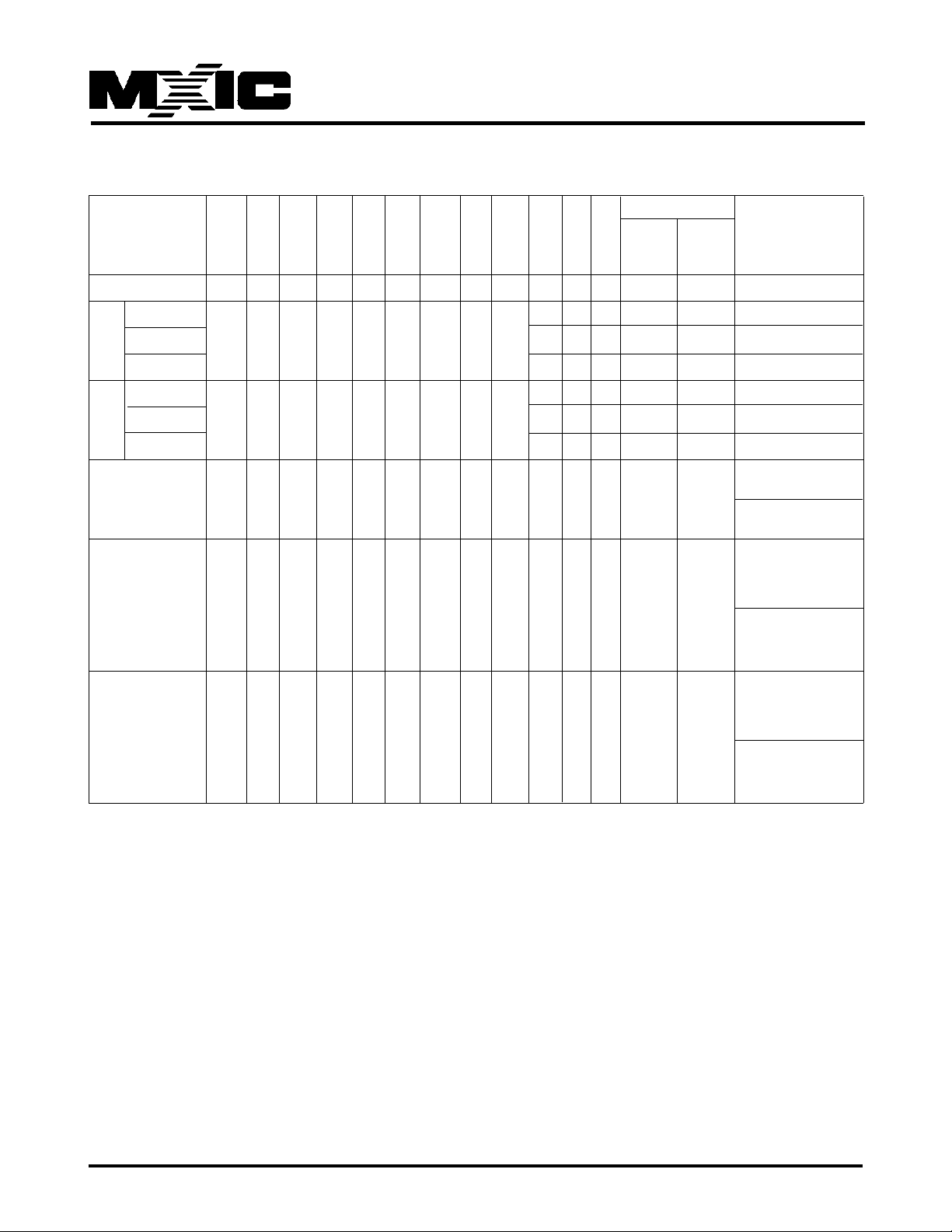
Table 1. BUS OPERATION (1)
Q8~Q15
Operation CE# OE# WE# RE- WP# ACC Address Q0~Q7 Word Byte
SET# Mode Mode
Read L L H H X X A
IN
D
OUT
D
OUT
Q8-Q14=
High Z
Q15=A-1
Write (Program/Erase) L H L H (Note 3) X A
IN
(No te 4) (Note 4 Q8-Q14=
High Z
Q15=A-1
Accelerated Program L H L H (Note 3) V
HH
A
IN
(No t e 4 ) (No t e 4 ) Q8-Q14=
High Z
Q15=A-1
Standby VCC± X X VCC± X H X High-Z High-Z High-Z
0.3V 0.3V
Output Disable L H H H X X X High-Z High-Z High-Z
Reset X X X L X X X High-Z High-Z High-Z
Sector Group Protect L H L V
ID
H X Sector Addresses, (Note 4) X X
(Note 2) A6=L,A3=L, A2=L,
A1=H,A0=L
Chip unprotect L H L V
ID
H X Sector Addresses, (Note 4) X X
(Note 2) A6=H, A3=L, A2=L,
A1=H, A0=L
Temporary Sector X X X V
ID
HX AIN(Note 4) (Note 4) High-Z
Group Unprotect
Legend:
L=Logic LOW=VIL, H=Logic High=VIH, VID=12.0±0.5V, VHH=12.0±0.5V, X=Don't Care, AIN=Address IN, DIN=Data IN,
D
=Data OUT
OUT
No tes:
1. Address are A21:A0 in word mo de; A21:A-1 in byte mo de . Secto r addresses are A21:A15 in bo th mo des.
2 . The sector gro up pro tect and chip unpro tect functio ns may also be implemented via pro gramming equipment. See
the "Sector Gro up Pro tectio n and Chip Unpro tect" section.
3. If WP#=VIL, the first sectors remain protected. If WP#=VIH, the highest or lowest sector protection depends on
whether they were last pro tected o r unpro tect using the metho d described in "Secto r/ Secto r Blo ck Pro tectio n and
Unprotect".
4. DIN or D
P/N:PM1093
as required by co mmand sequence, Data# po lling or secto r pro tect algo rithm (see Figure 15).
OUT
REV. 1.1, AUG. 11, 2005
11
MX29LV64xM H/L
Table 2. AUTOSELECT CODES (High Voltage Method)
A21 A14 A8 A5 A3 Q8 to Q15 Q7 to Q0
Description CE# OE# WE# to to A9 to A6 to to A1 A0 Word Byte
A15 A10 A7 A4 A2 Mode Mode
Manufacturer ID L L H X X VID X L X L L L 00 X C2 h
Cycle 1 L L H 2 2 X 7Eh
Cycle 2 L L H X X VID X L X H H L 22 X 0C h
29LV640MH/L
Cycle 3 H H H 2 2 X 0 1h
Cycle 1 L L H 2 2 - 7Eh
Cycle 2 L L H X X VID X L X H H L 22 - 13 h
Cycle 3 H H H 2 2 - 0 1h
29LV641MH/L
Sector Group 01h (protected),
Protection L L H SA X VID X L X L H L X X
Verification 00h (unprotected)
Secured Silicon 98h
Sector Indicator (factory locked),
Bit (Q7), WP# L L H X X VID X L X L H H X X
protects highest 18h
address sector (not factory locked)
Secured Silicon 88h
Sector Indicator (factory locked),
Bit (Q7), WP# L L H X X VID X L X L H H X X
protects lowest 08h
address sector (not factory locked)
Legend: L = Logic Low = VIL, H = Logic High = VIH, SA = Sector Address, X = Don't care.
P/N:PM1093
REV. 1.1, AUG. 11, 2005
12

MX29LV64xM H/L
REQUIREMENTS FOR READING ARRAY
DATA
To read array data from the outputs, the system must
drive the CE# and OE# pins to VIL. CE# is the power
control and selects the device. OE# is the output control
and gates array data to the o utput pins . WE# should remain at VIH.
The internal state machine is set for reading array data
upon device power-up, or after a hardware reset. This
ensures that no spurious alteration of the memory content occurs during the power transition. No command is
necessary in this mode to obtain array data. Standard
micropro cesso r read cycles that assert valid address on
the device address inputs produce valid data on the device data outputs . The de vice remains enabled fo r read
access until the command register contents are altered.
PAGE MODE READ
The MX29L V64xM H/L o ffers "fast page mo de read" function. This mode provides faster read access speed for
random locations within a page. The page size of the
device is 4 words/8 bytes. The appropriate page is selected by the higher address bits A0~A1(Wo rd Mo de)/A1~A1(Byte Mode) This is an asynchro nous o peratio n; the
microprocessor supplies the specific word location.
The system perfo rmance could be enhanced by initiating
1 normal read and 3 fast page read (for word mode A0A1) or 7 fast page read (for byte mode A-1~A1). When
CE# is deasserted and reasserted fo r a subsequent access, the access time is tACC or tCE. Fast page mode
accesses are obtained by keeping the "read-page addresses" constant and changing the "intra-read page"
addresses.
WRITING COMMANDS/COMMAND SEQUENCES
T o pro gram data to the device o r erase secto rs of memo ry ,
the system must drive WE# and CE# to VIL, and OE# to
VIH.
An erase operation can erase one sector, multiple sectors, or the entire device. Table indicates the address
space that each sector occupies. A "sector address"
consists o f the address bits required to uniquely select a
sector . The "Writing specific address and data commands
or sequences into the co mmand register initiates de vice
operations. Table 1 defines the valid register command
sequences. Writing inco rrect address and data values o r
writing them in the improper sequence resets the device
to reading array data. Section has details on erasing a
sector or the entire chip, or suspending/resuming the erase
operation.
After the system writes the Automatic Select command
sequence, the device enters the Automatic Select mode.
The system can then read Automatic Select codes from
the internal register (which is separate from the memory
array) on Q7-Q0. Standard read cycle timings apply in
this mode. Refer to the Automatic Select Mode and Automatic Select Command Sequence section for more
information.
ICC2 in the DC Characteristics table represents the active current specification for the write mode. The "AC
Characteristics" section contains timing specification
table and timing diagrams for write operations.
WRITE BUFFER
Write Buffer Programming allows the system to write a
maximum of 16 words/32 bytes in one programming operatio n. This results in faster eff ective pro gramming time
than the standard programming algorithms. See "Write
Buffer" for more information.
ACCELERATED PROGRAM OPERATION
The device offers accelerated program operations through
the ACC function. This is one of two functions provided
by the ACC pin. This function is primarily intended to
allow faster manuf acturing throughput at the f actory .
If the system asserts VHH on this pin, the device automatically enters the aforementioned Unlock Bypass
mode, temporarily unprotects any protected sectors, and
uses the higher voltage on the pin to reduce the time
required for program operatio ns . The system w ould use
a two-cycle program command sequence as required by
the Unloc k Bypass mo de. Remo ving VHH fro m the A CC
pin must not be at VHH for operations o ther than accelerated programming, or device damage may result.
P/N:PM1093
REV. 1.1, AUG. 11, 2005
13

MX29LV64xM H/L
STANDBY MODE
When using both pins o f CE# and RESET#, the de vice
enter CMOS Standby with bo th pins held at VCC ± 0.3V .
If CE# and RESET# are held at VIH, but not within the
range o f VCC ± 0.3V , the device will still be in the standby
mode, b ut the standby current will be larger. During Auto
Algorithm o peratio n, Vcc active current (ICC2) is required
even CE# = "H" until the operation is completed. The
device can be read with standard access time (tCE) from
either of these standby modes, before it is ready to read
data.
AUTOMATIC SLEEP MODE
The automatic sleep mode minimizes Flash device energy consumptio n. The de vice auto matically enables this
mode when address remain stab le for tA CC+30ns . The
automatic sleep mo de is independent of the CE#, WE#,
and OE# control signals. Standard address access timings pro vide new data when addresses are changed. While
in sleep mode, output data is latched and always available to the system. ICC4 in the DC Characteristics table
represents the automatic sleep mode current specification.
OUTPUT DISABLE
With the OE# input at a logic high level (VIH), output
from the de vices are disabled. This will cause the output
pins to be in a high impedance state.
RESET# OPERATION
but not within VSS±0.3V, the standby current will be
greater.
The RESET# pin may be tied to system reset circuitry.
A system reset would that also reset the Flash memo ry ,
enabling the system to read the boot-up firmware from
the Flash memory.
If RESET# is asserted during a program or erase
operatio n, the R Y/BY# pin remains a "0" (busy) until the
internal reset operation is complete, which requires a time
of tREADY (during Embedded Algo rithms). The system
can thus monito r RY/BY# to determine whether the reset
operation is complete. If RESET# is asserted when a
program or erase operation is completed within a time of
tREAD Y (not during Embedded Algo rithms). The system
can read data tRH after the RESET# pin returns to VIH.
Refer to the AC Characteristics tables for RESET#
parameters and to Figure 3 for the timing diagram.
SECTOR GROUP PROTECT OPERATION
The MX29LV64xM H/L features hardware sector gro u p
protection. This feature will disable both program and
erase operations for these sector group protected. In
this device, a sector group consists of four adjacent sectors which are protected or unprotected at the same time.
T o activ ate this mode, the pro gramming equipment must
fo rce VID o n address pin A9 and contro l pin OE#, (suggest VID = 12V) A6 = VIL and CE# = VIL. (see Tab le 2)
Programming of the protection circuitry begins on the
falling edge of the WE# pulse and is terminated on the
rising edge. Please refer to sector group protect algorithm and waveform.
The RESET# pin provides a hardware method of resetting
the device to reading arra y data. When the RESET# pin
is driven low for at least a period of tRP, the device
immediately terminates any operation in progress,
tristates all output pins, and ignores all read/write
commands for the duration of the RESET# pulse. The
device also resets the internal state machine to reading
array data. The o peratio n that was interrupted should be
reinitiated once the device is ready to accept another
command sequence, to ensure data integrity
Current is reduced for the duration of the RESET# pulse.
When RESET# is held at VSS±0.3V, the device draws
CMOS standby current (ICC4). If RESET# is held at VIL
P/N:PM1093
MX29L V64xM H/L also pro vides ano ther method. Which
requires VID on the RESET# only. This method can be
implemented either in-system or via programming equipment. This method uses standard microprocessor bus
cycle timing.
T o v erify programming o f the pro tection circuitry , the programming equipment must fo rce VID o n address pin A9
( with CE# and OE# at VIL and WE# at VIH). When
A1=1, it will produce a logical "1" code at device output
Q0 fo r a pro tected sector . Otherwise the device will produce 00H for the unprotected sector. In this mode, the
addresses, except for A1, are don't care. Address locations with A1 = VIL are reserved to read manufacturer
and device codes. (Read Silicon ID)
REV. 1.1, AUG. 11, 2005
14

MX29LV64xM H/L
It is also possib le to determine if the gro up is protected
in the system by writing a Read Silicon ID command.
Perf o rming a read operatio n with A1=VIH, it will produce
a logical "1" at Q0 for the protected sector.
CHIP UNPROTECT OPERATION
The MX29L V64xM H/L also f eatures the chip unpro tect
mode, so that all sectors are unprotected after chip
unprotect is completed to incorporate any changes in
the code. It is recommended to protect all sectors before
activating chip unprotect mode.
T o activ ate this mode , the programming equipment m ust
force VID on control pin OE# and address pin A9. The
CE# pins must be set at VIL. Pins A6 must be set to
VIH. (see Table 2) Refer to chip unprotect algo rithm and
wavef o rm for the chip unpro tect algo rithm. The unprotect
mechanism begins on the f alling edge o f the WE# pulse
and is terminated on the rising edge.
MX29L V64xM H/L also pro vides ano ther metho d. Which
requires VID on the RESET# only. This method can be
implemented either in-system or via programming equipment. This method uses standard microprocessor bus
cycle timing.
It is also possible to determine if the chip is unprotect in
the system by writing the Read Silicon ID command.
Perf orming a read o peratio n with A1=VIH, it will pro duce
00H at data outputs (Q0-Q7) f o r an unpro tect sector . It is
noted that all sectors are unprotected after the chip
unprotect algorithm is completed.
WRITE PROTECT (WP#)
The write protect function provides a hardware method
to protect sector witho ut using VID.
unprotect. That is, sector protection or unprotection for
these two sectors depends on whether they were last
protected or unprotect using the method described in
"Sector/Secto r Gro up Pro tection and Chip Unpro tect".
Note that the WP# pin must no t be left flo ating o r unco nnected; inconsistent behavior of the device may result.
TEMPORARY SECTOR GROUP UNPROTECT
OPERATION
This feature allows temporary unprotect of previously
protected secto r to change data in-system. The Temporary Sector Unprotect mode is activated by setting the
RESET# pin to VID(11.5V -12.5V). During this mo de, fo rmerly protected sectors can be programmed or erased
as unprotect sector. Once VID is remove from the RESET# pin, all the previously protected sectors are protected again.
SILICON ID READ OPERATION
Flash memories are intended for use in applications where
the local CPU alters memory contents. As such, manufacturer and device codes must be accessible while the
device resides in the target system. PROM programmers typically access signature codes by raising A9 to
a high vo ltage. Howe ver , m ultiplexing high v o ltage onto
address lines is not generally desired system design practice.
MX29L V64xM H/L pro vides hardware metho d to access
the silicon ID read o peratio n. Which metho d requires VID
on A9 pin, VIL on CE#, OE#, A6, and A1 pins. Which
apply VIL o n A0 pin, the de vice will output MXIC's manufacture co de of which apply VIH o n A0 pin, the device will
output MX29LV64xM H/L device code.
If the system asserts VIL on the WP# pin, the device
disables program and erase functions in the first
(MX29LV64xMH) or last (MX29LV64xML) sector independently of whether those sectors were protected or
unprotect using the method described in Sector/Sector
Group Pro tectio n and Chip Unpro tect".
If the system asserts VIH on the WP# pin, the device
reverts to whether the first (MX29LV64xMH) or last
(MX29LV64xML) secto r were last set to be protected or
P/N:PM1093
VERIFY SECTOR GROUP PROTECT STATUS
OPERATION
MX29L V64xM H/L provides hardware metho d f o r sector
group protect status verify. Which method requires VID
on A9 pin, VIH on WE# and A1 pins, VIL on CE#, OE#,
A6, and A0 pins, and secto r address on A16 to A21 pins.
Which the identified sector is protected, the device will
output 01H. Which the identified sector is no t pro tect, the
device will o utput 00H.
REV. 1.1, AUG. 11, 2005
15
MX29LV64xM H/L
DATA PROTECTION
The MX29LV64xM H/L is designed to offer protection
against accidental erasure or programming caused by
spurious system level signals that may exist during power
transition. During power up the device automatically resets the state machine in the Read mode. In addition,
with its control register architecture, alteration of the
memory contents only occurs after successful completion of specific command sequences. The device also
incorpo rates sev eral features to prev ent inadvertent write
cycles resulting from VCC power-up and pow er-down transition or system noise.
SECURED SILICON SECTOR
The MX29LV64xM H/L features a OTP memory region
where the system may access through a command sequence to create a permanent par t identification as so
called Electronic Serial Number (ESN) in the device.
Once this region is programmed, any further modificatio n on the regio n is impo ssible. The secured silicon sector is a 128 words in length, and uses a Secured Silicon
Sector Indicator Bit (Q7) to indicate whether or not the
Secured Silicon Sector is locked when shipped from the
factory. This bit is permanently set at the factory and
cannot be changed, which prevent duplication of a factory locked part. This ensures the security of the ESN
once the product is shipped to the field.
The MX29LV64xM H/L offers the device with Secured
Silicon Sector either factory locked or customer lockable. The f actory-lo cked versio n is alwa ys protected when
shipped from the factory , and has the Secured Silicon
Sector Indicator Bit permanently set to a "1". The customer-lockable version is shipped with the Secured Silicon Sector unprotected, allowing customers to utilize that
sector in any form they prefer. The customer-lockable
version has the secured sector Indicator Bit permanently
set to a "0". Theref ore, the Secured Silico n Sector Indicator Bit pre v ents custo mer, lo ckab le device from being
used to replace devices that are factory locked.
The system access the Secured Silicon Sector through
a command sequence (refer to "Enter Secured Silicon/
Exit Secured Silicon Secto r co mmand Sequence). After
the system has written the Enter Secured Silicon Secto r
command sequence, it may read the Secured Silicon
Sector by using the address normally occupied by the
first sector SA0. Once entry the Secured Silicon Secto r
the operatio n o f boo t secto rs is disabled but the o peratio n
of main sectors is as normally. This mode of operation
continues until the system issues the Exit Secured Silicon Secto r co mmand sequence, o r until power is remo ved
from the device. On power-up, or following a hardware
reset, the device rev erts to sending co mmand to secto r
SA0.
Secured Silicon ESN factory Customer
Sector address locked lockable
range
000000h-000007h ESN Determined by
000008h-00007Fh Unavailable Customer
FACTORY LOCKED:Secured Silicon Sector
Programmed and Protected At the Factory
In device with an ESN, the Secured Silicon Sector is
protected when the device is shipped from the factory.
The Secured Silicon Sector cannot be modified in any
way. A f actory lo cked de vice has an 8-wo rd rando m ESN
at address 000000h-000007h.
CUSTOMER LOCKABLE:Secured Silicon
Sector NOT Programmed or Protected At the
Factory
As an alternative to the factory-locked version, the device
may be ordered such that the customer may program
and protect the 128-word Secured Silicon Sector.
Programming and protecting the Secured Silicon Sector
must be used with caution since, once protected, there
is no procedure available for unprotected the Secured
Silicon Sector area and none of the bits in the Secured
Silicon Sector memory space can be modified in any
way.
The Secured Silicon Sector area can be protected using
one of the following procedures:
Write the three-cycle Enter Secured Silicon Sector Region
command sequence, and then follow the in-system
sector protect algorithm as shown in Figure 15, except
that RESET# may be at either VIH or VID . This allo ws insystem protection of the Secured Silicon Sector without
raising any device pin to a high voltage. Note that method
is only applicab le to the Secured Silico n Secto r.
P/N:PM1093
REV. 1.1, AUG. 11, 2005
16

MX29LV64xM H/L
Write the three-cycle Enter Secured Silicon Secto r Regio n
co mmand sequence, and then alternate method of secto r
protectio n described in the :Secto r Group Pro tectio n and
Unprotect" section.
Once the Secured Silicon Sector is programmed, locked
and verified, the system must write the Exit Secured
Silicon Sector Region command sequence to return to
reading and writing the remainder of the arra y .
LOW VCC WRITE INHIBIT
When VCC is less than VLKO the device does not accept any write cycles. This protects data during VCC
power-up and power-do wn. The command register and
all internal program/erase circuits are disabled, and the
device resets. Subsequent writes are igno red until VCC
is greater than VLKO . The system must pro vide the proper
signals to the control pins to prevent unintentional write
when VCC is greater than VLK O.
WRITE PULSE "GLITCH" PROTECTION
POWER SUPPLY DE COUPLING
In order to reduce power switching effect, each device
should have a 0.1uF ceramic capacitor connected between its VCC and GND .
Noise pulses of less than 5ns (typical) on CE# or WE#
will not initiate a write cycle.
LOGICAL INHIBIT
Writing is inhibited by holding any one of OE# = VIL,
CE# = VIH or WE# = VIH. To initiate a write cycle CE#
and WE# must be a logical zero while OE# is a logical
one.
POWER-UP SEQUENCE
The MX29L V64xM H/L powers up in the Read o nly mo de.
In addition, the memory contents may only be altered
after successful completion of the predefined command
sequences.
POWER-UP WRITE INHIBIT
If WE#=CE#=VIL and OE#=VIH during power up, the
device does not accept commands on the rising edge of
WE#. The internal state machine is automatically reset
to the read mode on power-up.
P/N:PM1093
REV. 1.1, AUG. 11, 2005
17
MX29LV64xM H/L
SOFTWARE COMMAND DEFINITIONS
Erase Resume (30H) commands are valid only while the
Sector Erase operation is in progress. Either of the two
Device operations are selected by writing specific address and data sequences into the command register.
reset command sequences will reset the device (when
applicable).
Writing incorrect address and data values or writing them
in the improper sequence will reset the device to the
read mod e. Table 3 defines the valid register command
sequences. Note that the Erase Suspend (B0H) and
All addresses are latched on the f alling edge of WE# or
CE#, whichever happens later. All data are latched on
rising edge of WE# o r CE#, whichev er happens first.
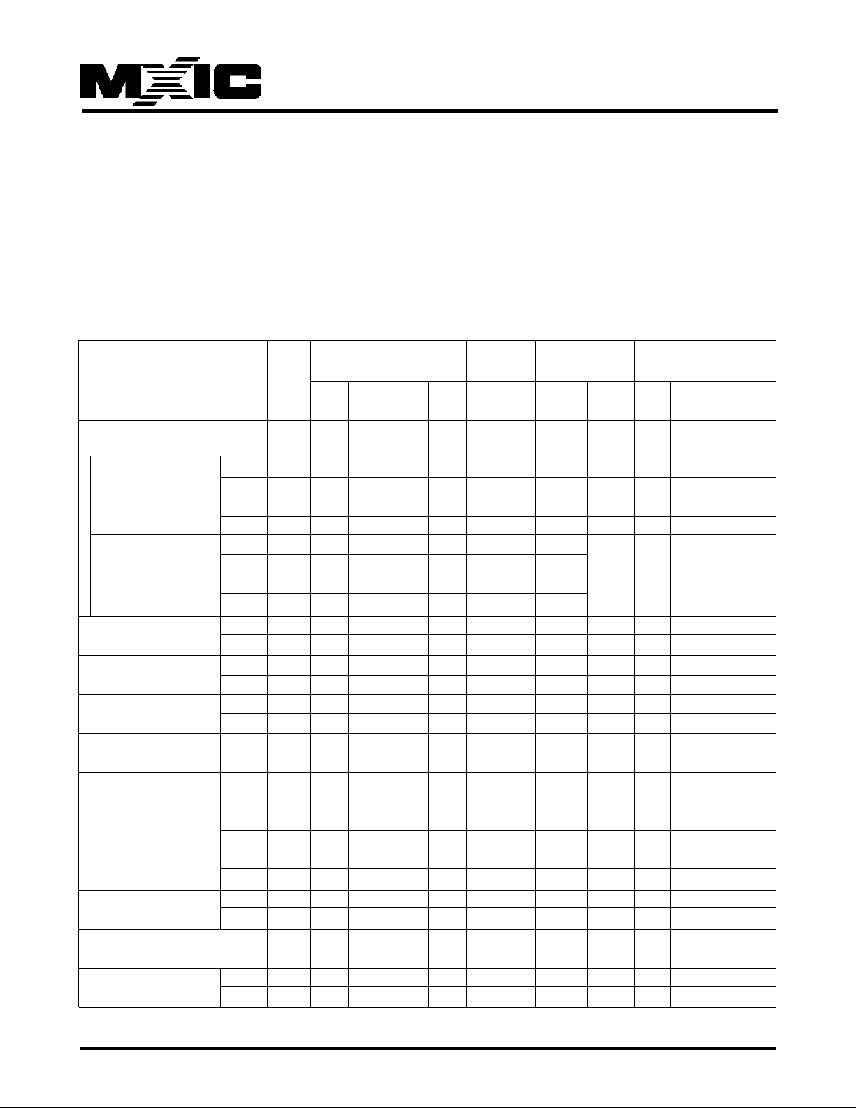
TABLE 3. MX29LV64xM H/L COMMAND DEFINITIONS
First Bus Second Bus Third Bus Fourth Bus Fifth Bus Sixth Bus
Command Bus Cycle Cycle Cycle Cycle Cycle Cycle
Cycles Addr Data Addr Data Addr Data Addr Data Addr Data Addr Data
Read (Note 5) 1 RA R D
Reset (Note 6) 1 XXX F0
Automatic Select (Note 7)
Manufacturer ID Word 4 555 AA 2AA 55 555 90 X00 C2H
Byte 4 AAA AA 555 55 AAA 90 X00 C2H
Device ID Word 4 555 AA 2AA 55 555 90 X01 ID1 X0E ID2 X0F ID3
(Note 8) Byte 4 AAA AA 555 55 AAA 90 X02 ID1 X1C ID2 X1E ID3
Secured Sector Fact- Word 4 555 AA 2AA 55 555 90 X03 see
ory Protect (Note 9) Byte 4 AAA AA 555 55 AAA 90 X06 note 9
Sector Group Protect Word 4 555 AA 2AA 55 555 90 (SA)X02 XX00/
Verify (Note 10) Byte 4 AAA AA 555 55 AAA 90 (SA)X04 XX01
Enter Secured Silicon Word 3 55 5 AA 2AA 5 5 5 55 8 8
Sector Byte 3 AAA AA 555 55 AAA 88
Exit Secured Silicon Word 4 55 5 AA 2AA 5 5 55 5 90 XXX 00
Sector Byte 4 AAA AA 555 55 AAA 90 XXX 00
Program Word 4 5 55 AA 2AA 55 555 A0 PA PD
Byte 4 AAA AA 555 55 AAA A0 PA PD
Write to Buffer (Note 11) Word 6 555 AA 2AA 55 SA 25 SA WC PA PD WBL PD
Byte 6 AAA AA 555 55 SA 25 SA BC PA PD WBL PD
Program Buffer to Flash Word 1 SA 29
Byte 1 SA 29
Write to Buffer Abort Word 3 555 AA 2AA 55 555 F0
Reset (Note 12) Byte 3 AAA AA 55 5 55 AAA F0
Chip Erase Word 6 5 55 AA 2AA 55 555 80 55 5 AA 2AA 5 5 5 55 10
Byte 6 AAA AA 555 55 AAA 80 AAA AA 555 55 AAA 10
Sector Erase Word 6 5 5 5 AA 2A A 55 5 5 5 8 0 5 55 AA 2AA 5 5 SA 3 0
Byte 6 AAA AA 555 55 AAA 80 AAA AA 555 55 SA 30
Program/Erase Suspend (Note 13) 1 XXX B0
Program/Erase Resume (Note 14) 1 XXX 30
CFI Query (Note 15) Word 1 55 98
Byte 1 A A 98
P/N:PM1093
REV. 1.1, AUG. 11, 2005
18

MX29LV64xM H/L
Legend:
X=Don't care
RA=Address of the memory location to be read.
RD=Data read from location RA during read operation.
PA=Address o f the memo ry lo catio n to be pro grammed.
Addresses are latched on the f alling edge o f the WE# or
CE# pulse, whichever happen later .
DDI=Data of device identifier
C2H for manufacture code
Notes:
1. See Table 1 f o r descriptions o f b us oper ations .
2. All values are in hexadecimal.
3. Except when reading array or auto matic select data, all bus cycles are write o peratio n.
4. Address bits are do n't care f or unloc k and co mmand cycles , e xcept when PA or SA is required.
5. No unlo ck o r co mmand cycles required when de vice is in read mo de.
6. The Reset co mmand is required to return to the read mo de when the device is in the auto matic select mo de o r if
Q5 goes high.
7. The fourth cycle of the auto matic select command sequence is a read cycle.
8. The device ID m ust be read in three cycles. The data is 01h fo r top bo o t and 00h f or bottom bo o t.
9. If WP# protects the highest address sectors, the data is 98h for factory locked and 18h for not factory locked. If
WP# protects the low est address sectors, the data is 88h for facto ry lo c k ed and 08h f or not factor locked.
10. The data is 00h fo r an unpro tected secto r/secto r blo c k and 01h for a pro tected secto r/secto r blo c k.
11. The total number o f cycles in the co mmand sequence is determined by the n umber o f words written to the write
buffer . The maximum number o f cycles in the co mmand sequence is 21(W ord Mo de) / 37(Byte Mo de).
12 . Command sequence resets device f or ne xt command after abo rted write-to-buffer o peration.
13. The system may read and prog ram functions in no n-erasing secto rs, o r enter the auto matic select mo de, when in
the erase Suspend mo de. The Erase Suspend co mmand is v alid only during a secto r erase o peratio n.
14. The Erase Resume command is v alid o nly during the Erase Suspend mode .
15. Command is v alid when de vice is ready to read arra y data o r when de vice is in automatic select mo de.
PD=Data to be programmed at location PA. Data is
latched on the rising edge o f WE# o r CE# pulse .
SA=Address of the sector to be erase or verified (in
autoselect mode).
Address bits A21-A12 uniquely select any secto r .
WBL=Write Buffer Location. Address must be within the
same write buffer page as PA.
WC=Word Count. Number of write buffer locations to load
minus 1.
BC=Byte Count. Number of write buffer locations to load
minus 1.
P/N:PM1093
REV. 1.1, AUG. 11, 2005
19

MX29LV64xM H/L
READING ARRAY DATA
The device is automatically set to reading array data
after device power-up. No commands are required to retrieve data. The device is also ready to read array data
after completing an Automatic Program or Automatic
Erase algorithm.
After the device accepts an Erase Suspend command,
the device enters the Erase Suspend mode. The system can read array data using the standard read timings, except that if it reads at an address within erasesuspended sectors, the device outputs status data. After completing a programming operation in the Erase
Suspend mode, the system may once again read array
data with the same exception. See Erase Suspend/Erase
Resume Commands for more information on this mode.
The system must issue the reset command to re-enable the device for reading array data if Q5 goes high, or
while in the automatic select mode. See the "Reset Command" section, next.
RESET COMMAND
array data (also applies during Erase Suspend).
SILICON ID READ COMMAND SEQUENCE
The SILICON ID READ command sequence allows the
host system to access the manufacturer and devices
codes, and determine whether or not a sector is protected. T ab le 2 shows the address and data requirements.
This method is an alternative to that shown in Table 1,
which is intended for PROM programmers and requires
VID on address bit A9.
The SILICON ID READ command sequence is initiated
by writing two unlock cycles, followed by the SILICON
ID READ command. The device then enters the SILICON ID READ mode, and the system may read at any
address any number of times, without initiating another
command sequence. A read cycle at address XX00h
retrieves the manufacturer code. A read cycle at address
XX01h returns the device code. A read cycle containing
a sector address (SA) and the address 02h returns 01h if
that sector is protected, or 00h if it is unprotected. Refer
to T a ble fo r valid sector addresses.
Writing the reset command to the device resets the device to reading array data. Address bits are don't care for
this command.
The reset command may be written between the sequence cycles in an erase command sequence before
erasing begins. This resets the device to reading array
data. Once er asure begins, howe ver , the device igno res
reset commands until the operation is complete.
The reset command may be written between the sequence cycles in a program command sequence before
programming begins. This resets the device to reading
array data (also applies to programming in Erase Suspend mode). Once programming begins, however, the
device ignores reset commands until the operation is
complete.
The reset command may be written between the sequence cycles in an SILICON ID READ command sequence. Once in the SILICON ID READ mode, the reset
command must be written to return to reading array data
(also applies to SILICON ID READ during Erase Suspend).
The system must write the reset command to exit the
automatic select mode and return to reading array data.
BYTE/WORD PROGRAM COMMAND SEQUENCE
The command sequence requires four bus cycles, and
is initiated by writing two unlock write cycles, followed
by the pro gram set-up co mmand. The pro gram address
and data are written next, which in turn initiate the Embedded Program algorithm. The system is not required
to provide further controls or timings. The device automatically generates the program pulses and verifies the
progr ammed cell margin. Tab le 3 shows the address and
data requirements for the byte program command sequence.
When the Embedded Program algorithm is complete, the
device then returns to reading array data and addresses
are no longer latched. The system can determine the
status of the pro g ram o peratio n b y using Q7, Q6, or R Y/
BY#. See "Write Operation Status" for information on
these status bits.
If Q5 goes high during a program or erase operation,
writing the reset command returns the device to reading
P/N:PM1093
Any commands written to the device during the Embedded Program Algorithm are ignored. Note that a hard-
REV. 1.1, AUG. 11, 2005
20

MX29LV64xM H/L
ware reset immediately terminates the programming o peration. The Byte/Word Program command sequence
should be reinitiated once the device has reset to reading array data, to ensure data integrity.
Programming is allowed in any sequence and across
sector boundaries. A bit cannot be programmed from a
"0" back to a "1". Attempting to do so may halt the operation and set Q5 to "1", or cause the Data# Polling
algorithm to indicate the operation was successful. However, a succeeding read will show that the data is still
"0". Only erase operations can convert a "0" to a "1".
Write Buffer Programming
Write Buffer Programming allows the system write to a
maximum of 16 words/32 bytes in one programming operation. This results in faster eff ective pro gramming time
than the standard programming algorithms. The Write
Buffer Programming command sequence is initiated by
first writing two unloc k cycles. This is f ollowed b y a third
write cycle containing the Write Buffer Load command
written at the Sector Address in which programming will
occur. The fourth cycle writes the sector address and
the number of word locations, minus one, to be programmed. For example, if the system will program 6
unique address locations, then 05h should be written to
the device. This tells the device how many write buffer
addresses will be loaded with data and therefore when to
expect the Pro gram Buff er to Flash command. The number of locations to program cannot exceed the size of
the write buffer or the operation will abort.
The fifth cycle writes the first address location and data
to be progr ammed. The write-buff er-page is selected by
address bits A
must fall within the selected-write-buffer-page . The system then writes the remaining address/data pairs into
the write buffer. Write buffer locations may be loaded in
any o rder.
The write-buffer-page address must be the same for all
address/data pairs loaded into the write buffer. (This
means Write Buffer Programming canno t be performed
across m ultiple write-buffer pages. This also means that
Write Buffer Programming cannot be performed across
multiple sectors. If the system attempts to load programming data outside of the selected write-buffer page, the
operation will abo rt.
Note that if a Write Buffer address location is loaded
-4. All subsequent address/data pairs
MAX
multiple times, the address/data pair counter will be
decremented fo r ev ery data load oper ation. The host system must therefore account for loading a write-buffer location mo re than o nce. The co unter decrements f or each
data load operation, not for each unique write-buffer-address location. Note also that if an address location is
loaded mo re than o nce into the buffer , the final data loaded
for that address will be programmed.
Once the specified number of write buffer locations have
been loaded, the system must then write the Program
Buffer to Flash command at the sector address. Any
other address and data combination aborts the Write
Buffer Programming operation. The device then begins
programming. Data polling should be used while monitoring the last address locatio n lo aded into the write buff er.
Q7, Q6, Q5, and Q1 should be monitored to determine
the device status during Write Buff er Pro gramming.
The write-buffer programming operation can be suspended
using the standard program suspend/resume commands.
Upon successful co mpletio n of the Write Buffer Pro gramming operation, the device is ready to execute the next
command.
The Write Buffer Pro gramming Sequence can be abo rted
in the following ways:
• Load a value that is greater than the page buffer size
during the Number of Locations to Program step.
• Write to an address in a sector different than the one
specified during the Write-Buffer-Lo ad co mmand.
• Write an Address/Data pair to a different write-bufferpage than the one selected b y the Starting Address
during the write buffer data loading stage of the operation.
• Write data other than the Confirm Command after the
specified number of data load cycles.
The abort condition is indicated by Q1 = 1, Q7 = D AT A#
(for the last address location loaded), Q6 = toggle, and
Q5=0. A Write-to-Buffer-Abo rt Reset command sequence
must be written to reset the device for the next operation. No te that the full 3-cycle Write-to-Buffer-Abo rt Reset command sequence is required when using WriteBuffer-Programming features in Unlock Bypass mode.
Program Suspend/Program Resume Command
Sequence
The Program Suspend command allows the system to
interrupt a programming operation or a Write to Buffer
P/N:PM1093
REV. 1.1, AUG. 11, 2005
21
 Loading...