MX COM Inc MX929D5, MX929E2, MX929P4 Datasheet
COMMUNICATION SEMICONDUCTORS
CMX969
DATA BULLETIN
MOTIENT
SM
/ARDIS
SM
RD-LAP
TM
MDC4800 Modem
Radio Data-Link Access Procedure (RD-LAP) is a data communications air interface protocol developed by Motorola Inc.
MOTIENT is a registered service mark of the MOTIENT Company operating the MOTIENT Network. (Formerly known as American Mobile, operating the ARDIS Network).
DataTAC is a registered trademark of Motorola Inc.
¤¤¤¤2001 MX-COM, Inc. www.mxcom.com Tel: 800 638 5577 336 744 5050 Fax: 336 744 5054 Doc. # 20480211.002
4800 Bethania Station Road, Winston-Salem, NC 27105-1201 USA All trademarks and service marks are held by their respective companies.
Advance Information
Features Applications
• Autonomous Frame Sync
Detection for SFR operation
• Full Packet Data Framing
• Powersave Option
• Low Power, 3.0 to 5.5V operation
• DataTACTM, MOTIENTSM/ARDISSM,
Dual Mode
(RD-LAPTM and MDC4800 Systems)
• Two-Way Paging Equipment
• Mobile Data Systems
• Wireless Telemetry
• DataTACTM Terminals
MODEM
DATA
PUMP
ANALOG Tx
DATA AND
CONTROL
BUS
ANALOG Rx
RF
RADIO
DISCRIMINATOR
MODULATOR
SYSTEM
APPLICATION
PROCESSING
HOST C
CMX969
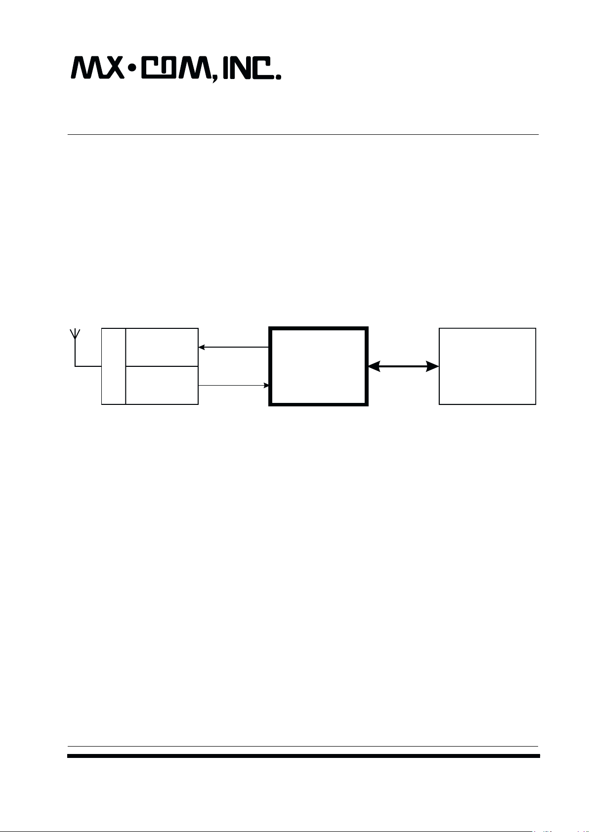
The CMX969 is a CMOS integrated circuit that contains all of the baseband signal processing and Medium
Access Control (MAC) protocol functions required for a high performance DataTAC dual mode (RD-LAP
19.2kbps and MDC4800 4.8kbps) FSK Wireless Packet Data Modem suitable for use with the
MOTIENT/ARDIS network. It interfaces with the modem host processor and the radio
modulation/demodulation circuits to deliver reliable two-way transfer of the application data over the wireless
link.
The CMX969 assembles application data received from the host processor, adds forward error correction
(FEC) and error detection (CRC) information and interleaves the result for burst-error protection. After adding
symbol and frame synchronization codewords and channel status symbols, it converts the packet into a
filtered analog baseband signal for modulating the radio transmitter.
In receive mode, the CMX969 performs the reverse function using the analog baseband signals from the
receiver frequency discriminator. After error correction and removal of the packet overhead, the recovered
application data is supplied to the host processor. Any residual uncorrected errors in the data will be flagged.
A readout of the received signal quality is also provided.
An optional Autonomous Frame Sync Detection function is provided for use in MOTIENT/ARDIS systems
employing Single Frequency Re-use operation.
The CMX969 uses signal filtering, data block formats and FEC/CRC algorithms compatible with the MDC and
RD-LAP over-air standards. The device is programmable to operate from a wide choice of Xtal frequencies
and is available in 24-pin PDIP (CMX969P4), 24-pin SSOP (CMX969D5), and 24-pin TSSOP (CMX969E2)
packages.

MOTIENTSM/ARDIS
SM
RD-LAP
TM
MDC4800 Modem 2 CMX969 Advance Information
¤¤¤¤2001 MX-COM, Inc. www.mxcom.com Tel: 800 638 5577 336 744 5050 Fax: 336 744 5054 Doc. # 20480211.002
4800 Bethania Station Road, Winston-Salem, NC 27105-1201 USA All trademarks and service marks are held by their respective companies.
CONTENTS
Section Page
1 Block Diagram ............................................................................................................... 4
2 Signal List...................................................................................................................... 5
3 External Components ................................................................................................... 6
4 General Description ...................................................................................................... 7
4.1 Description of Blocks .........................................................................................................7
4.1.1 Data Bus Buffers..................................................................................................................... 7
4.1.2 Address and R/W Decode ...................................................................................................... 7
4.1.3 Status and Data Quality Registers.......................................................................................... 7
4.1.4 Command, Mode and Control Registers ................................................................................ 7
4.1.5 Data Buffer.............................................................................................................................. 7
4.1.6 CRC Generator/Checker ........................................................................................................ 7
4.1.7 FEC Encoder/Decoder............................................................................................................ 7
4.1.8 Interleave/De-interleave Buffer............................................................................................... 8
4.1.9 Auto Frame Sync Detect, Rx Level & Timing Extraction, Rx Data Symbol Extraction........... 8
4.1.10 Rx Input Amp .......................................................................................................................... 8
4.1.11 Low Pass Filter ....................................................................................................................... 8
4.1.12 Tx Output Buffer...................................................................................................................... 8
4.1.13 Clock Oscillator and Dividers.................................................................................................. 8
4.2 Modem - µC Interaction ..................................................................................................... 9
4.3 Binary to RD-LAP 4-Level Symbol Translation................................................................... 9
4.4 Frame Structure............................................................................................................... 10
4.4.1 MDC Mode............................................................................................................................ 10
4.4.2 RD-LAP Mode....................................................................................................................... 11
4.5 The Programmer's View................................................................................................... 12
4.5.1 Data Block Buffer .................................................................................................................. 12
4.5.2 Control Register .................................................................................................................... 12
4.5.3 Mode Register....................................................................................................................... 13
4.5.4 Command Register ............................................................................................................... 14
4.6 CMX969 Modem Tasks ................................................................................................... 16
4.6.1 Transmit Mode ...................................................................................................................... 16
4.6.2 Receive Mode: ...................................................................................................................... 19
4.6.3 Task Timings......................................................................................................................... 22
4.6.4 Lowpass Filter Delay ............................................................................................................24
4.6.5 Status Register ..................................................................................................................... 24
4.6.6 Data Quality Register............................................................................................................ 26

MOTIENTSM/ARDIS
SM
RD-LAP
TM
MDC4800 Modem 3 CMX969 Advance Information
¤¤¤¤2001 MX-COM, Inc. www.mxcom.com Tel: 800 638 5577 336 744 5050 Fax: 336 744 5054 Doc. # 20480211.002
4800 Bethania Station Road, Winston-Salem, NC 27105-1201 USA All trademarks and service marks are held by their respective companies.
5 Application Notes........................................................................................................ 27
5.1 Autonomous Frame Sync Detect Function....................................................................... 27
5.2 Rx Control Procedure ...................................................................................................... 28
6 Performance Specification......................................................................................... 29
6.1 Electrical Performance..................................................................................................... 29
6.1.1 Absolute Maximum Ratings .................................................................................................. 29
6.1.2 Operating Limits.................................................................................................................... 29
6.1.3 Operating Characteristics ..................................................................................................... 30
6.2 Packaging........................................................................................................................ 34
MX-COM, Inc. reserves the right to change specifications at any time and without notice.
MOTIENTSM/ARDIS
SM
RD-LAP
TM
MDC4800 Modem 4 CMX969 Advance Information
¤¤¤¤2001 MX-COM, Inc. www.mxcom.com Tel: 800 638 5577 336 744 5050 Fax: 336 744 5054 Doc. # 20480211.002
4800 Bethania Station Road, Winston-Salem, NC 27105-1201 USA All trademarks and service marks are held by their respective companies.
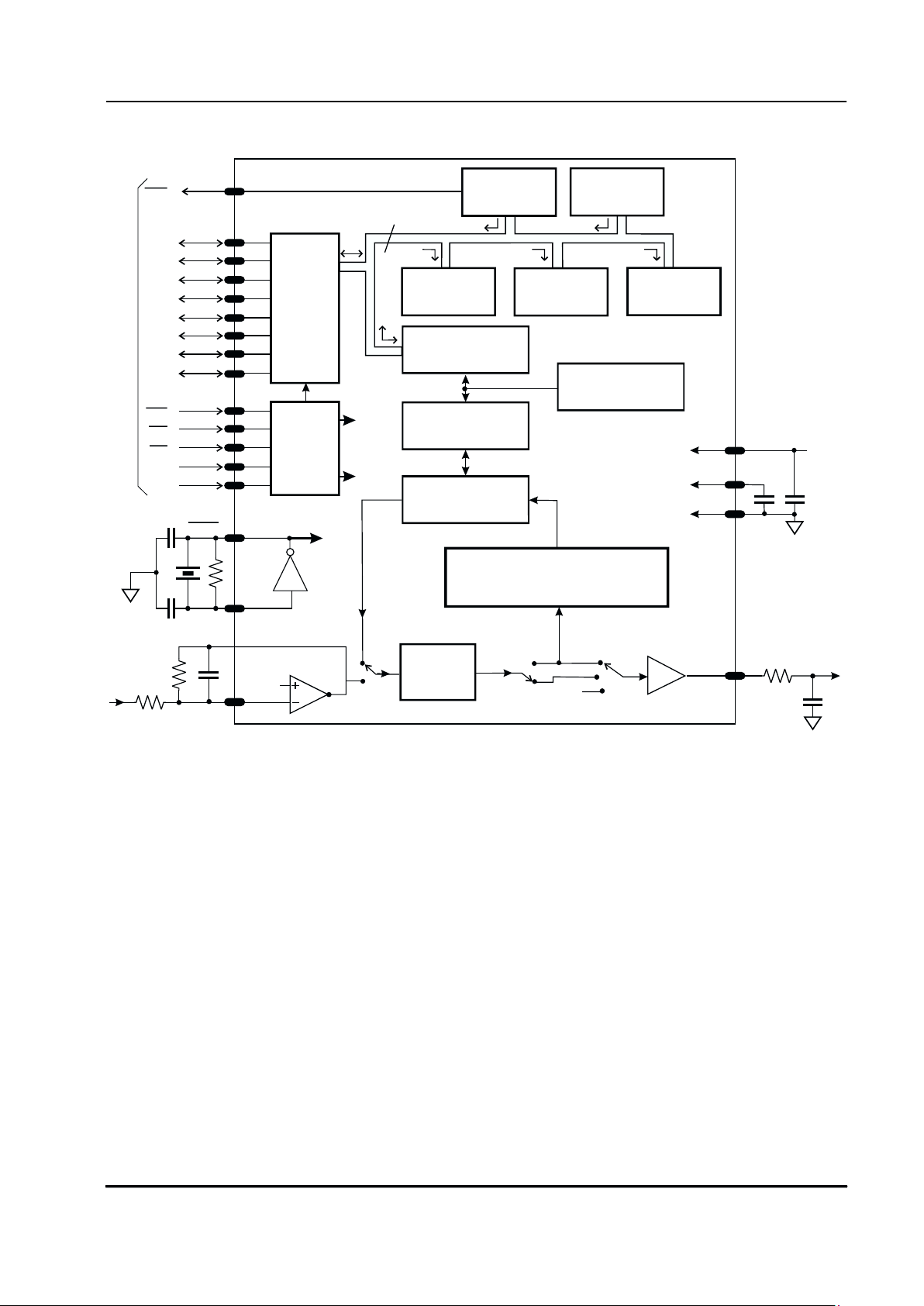
1 Block Diagram
V
BIAS
V
BIAS
TXOUT
To FM Modulator
RXIN
Rx Input Amp
Tx Output Buffer
D0
D1
D2
D3
D4
D5
D6
D7
A0
A1
8
Tx
Tx
Symbols
Rx
Symbols
Tx
Rx
RxEye
Tx
Rx
Rx
V
BIAS
CONTROLLER INTERFACE
DATA
BUS
BUFFERS
ADDRESS
AND
R/W
DECODE
FEC
ENCODER/
DECODER
INTERLEAVE/
DE-INTERLEAVE
AUTO FRAME SYNC DETECT,
Rx LEVEL & TIMING EXTRACTION,
Rx DATA SYMBOL EXTRACTION
IRQ
WR
RD
CS
CONTROL
REGISTER
MODE
REGISTER
COMMAND
REGISTER
DATA BLOCK
BUFFER
STATUS
REGISTER
DATA
QUALITY
REGISTER
LOW PASS
FILTER
XTAL
RXFB
From FM
Demod
V
DD
V
SS
XTAL
Clock oscillator
and dividers
CRC
GENERATOR/
CHECKER
Figure 1: Block Diagram
MOTIENTSM/ARDIS
SM
RD-LAP
TM
MDC4800 Modem 5 CMX969 Advance Information
¤¤¤¤2001 MX-COM, Inc. www.mxcom.com Tel: 800 638 5577 336 744 5050 Fax: 336 744 5054 Doc. # 20480211.002
4800 Bethania Station Road, Winston-Salem, NC 27105-1201 USA All trademarks and service marks are held by their respective companies.
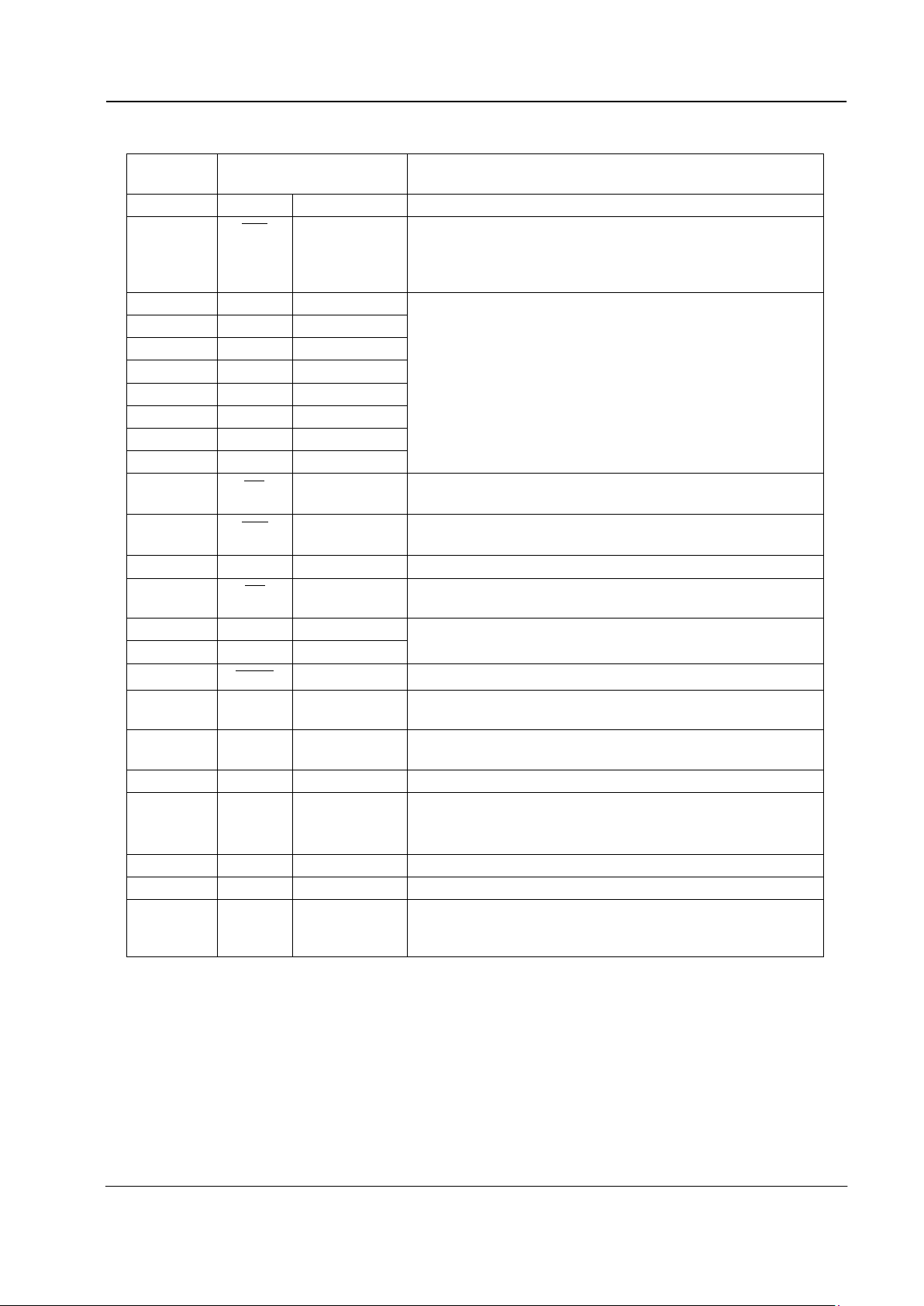
2 Signal List
Package
P4/E2/D5
Signal Description
Pin No. Name Type
1
IRQ
output
A 'wire-ORable' output for connection to the host
µC's
Interrupt Request input. This output has a low impedance
pull down to V
SS
when active and is high impedance when
inactive.
2 D7 bi-directional
3 D6 bi-directional
4 D5 bi-directional
5 D4 bi-directional
6 D3 bi-directional
7 D2 bi-directional
8 D1 bi-directional
9 D0 bi-directional
8-bit bi-directional 3-state
µC interface data lines.
10
RD
input Read: An active low logic level input used to control the
reading of data from the modem into the host
µC.
11
WR
input Write: An active low logic level input used to control the
writing of data into the modem from the host
µC.
12 VSS power The negative supply rail (ground).
13
CS
input Chip Select: An active low logic level input to the modem,
used to enable a data read or write operation.
14 A0 input
15 A1 input
Two logic level modem register select inputs.
16
XTAL
output The output of the on-chip oscillator.
17 XTAL input The input to the on-chip oscillator, for external Xtal circuit or
clock.
18,19 NC No connection should be made to these pins (reserved for
possible future use)
20 TXOUT output The Tx signal output from the modem.
21 V
BIAS
output A bias line for the internal circuitry, held at VDD/2.
This pin must be decoupled to V
SS
by a capacitor mounted
close to the device pins.
22 RXIN input The input to the Rx input amplifier.
23 RXFB output The output of the Rx input amplifier.
24 VDD power The positive supply rail. Levels and voltages are dependent
upon this supply. This pin should be decoupled to V
SS
by a
capacitor.
Table 1: Signal List
Note: Internal protection diodes are connected from each signal pin to V
DD
and V
SS
.
MOTIENTSM/ARDIS
SM
RD-LAP
TM
MDC4800 Modem 6 CMX969 Advance Information
¤¤¤¤2001 MX-COM, Inc. www.mxcom.com Tel: 800 638 5577 336 744 5050 Fax: 336 744 5054 Doc. # 20480211.002
4800 Bethania Station Road, Winston-Salem, NC 27105-1201 USA All trademarks and service marks are held by their respective companies.
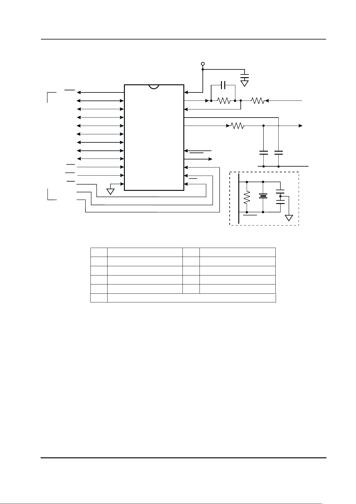
3 External Components
V
DD
V
DD
V
SS
V
BI AS
RXIN
FROM Rx FM
DISCRIMINATOR
TO Tx
FREQUENCY
MODULATOR
RXFB
V
SS
WR
IRQ
RD
CS
CS
R2
R4
R1
µCONTROLLER INTERFACE
CMX969
P4/E2/D5
TXOUT
C5
C3
C4
R3
X1
C1
C6
C2
D7
D6
D5
D4
D3
D2
D1
D0
A0
A1
A1
A0
XTAL
XTAL
XTAL
XTAL
1
2
3
4
5
6
8
9
10
11
12
13
14
7
24
23
22
21
20
19
18
17
17
16
16
15
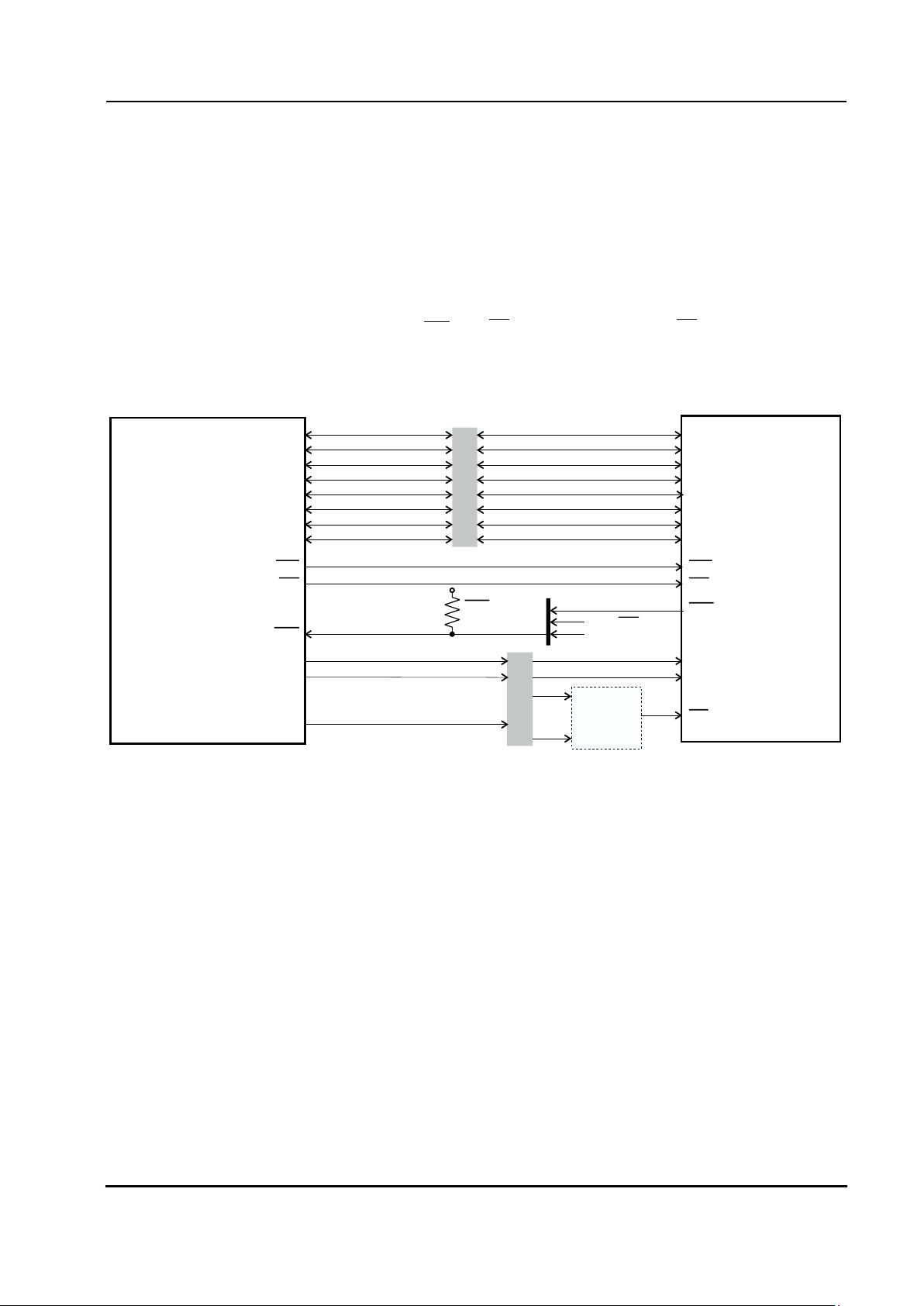
Figure 2: Recommended External Components
R1 See Section 4.1 C2
0.1 µF
± 20%
R2
100k
Ω ± 5%
C3
± 20%, see Note 1
R3
1M
Ω ± 20%
C4
± 20%, see Note 1
R4
100k
Ω ± 5%
C5
100pF ± 5%
C1
0.1 µF
± 20%
C6
100pF ± 5%
X1 4.9152, 7.3728 or 9.8304 MHz ±100ppm. See Section 4.5.2
Table 2: Recommended External Components
Recommended External Component Notes:
1. The values used for C3 and C4 should be suitable for the frequency of the crystal X1. As a guide, values
(including stray capacitances) of 33pF at 1MHz falling to 18pF at 10MHz will generally prove suitable.
2. For best results, a crystal oscillator design should drive the clock inverter input with signal levels of at
least 40% of V
DD
, peak to peak. Tuning fork crystals generally cannot meet this requirement. To obtain
crystal oscillator design assistance, please consult your crystal manufacturer.
MOTIENTSM/ARDIS
SM
RD-LAP
TM
MDC4800 Modem 7 CMX969 Advance Information
¤¤¤¤2001 MX-COM, Inc. www.mxcom.com Tel: 800 638 5577 336 744 5050 Fax: 336 744 5054 Doc. # 20480211.002
4800 Bethania Station Road, Winston-Salem, NC 27105-1201 USA All trademarks and service marks are held by their respective companies.
4 General Description
4.1 Description of Blocks
Refer to Figure 1.
4.1.1 Data Bus Buffers
Eight bi-directional 3-state logic level buffers between the modem's internal registers and the host µC's data
bus lines.
4.1.2 Address and R/W Decode
This block controls the transfer of data bytes between the µC and the modem's internal registers, according to
the state of the Write and Read Enable inputs (
WR and RD ), the Chip Select input ( CS ) and the Register
Address inputs A0 and A1.
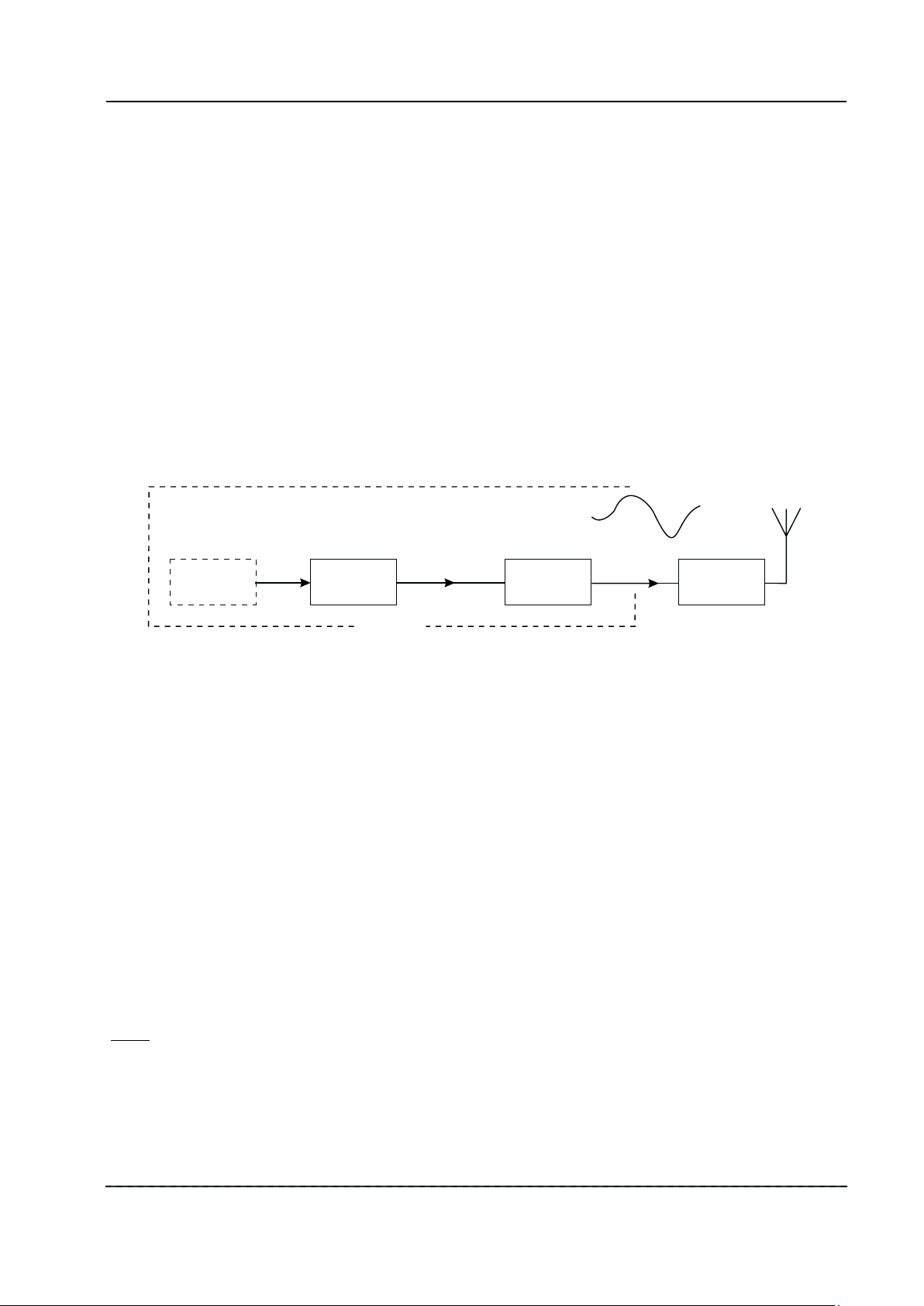
The Data Bus Buffers, Address and R/W Decode blocks provide a byte-wide parallel µC interface, which can
be memory-mapped, as shown in Figure 3.
MODEM
other inputs
to µController
IRQ
.
.
.
.
.
.
.
.
.
.
.
.
.
.
.
WR WR
RD RD
IRQ
IRQ
IRQ pull up
resistor
V
DD
A0 A0
A1 A1
An
CS
µCONTROLLER
µC Address Bus
µC Data Bus
Modem
Address
Decode
D0 D0
D1
D2
D3
D4
D5
D6
D7
D1
D2
D3
D4
D5
D6
D7
Figure 3: Typical Modem µµµµC Connections
4.1.3 Status and Data Quality Registers
Two 8-bit registers which the µC can read to determine the status of the modem and the received data
quality.
4.1.4 Command, Mode and Control Registers
The values written by the µC to these 8-bit registers control the operation of the modem.
4.1.5 Data Buffer
A 12-byte buffer used to hold receive or transmit data to or from the µC.
4.1.6 CRC Generator/Checker
A circuit which generates (in transmit mode) or checks (in receive mode) the Cyclic Redundancy Checksum
bits, which are included in transmitted data blocks so that the receive modem can detect transmission errors.
4.1.7 FEC Encoder/Decoder
In transmit mode, this circuit adds Forward Error Correction information to the transmitted data. In RD-LAP
mode it also converts the binary data to 4-level symbols. In receive mode, this block translates received
symbols to binary data, using the FEC information to correct a large proportion of transmission errors.
MOTIENTSM/ARDIS
SM
RD-LAP
TM
MDC4800 Modem 8 CMX969 Advance Information
¤¤¤¤2001 MX-COM, Inc. www.mxcom.com Tel: 800 638 5577 336 744 5050 Fax: 336 744 5054 Doc. # 20480211.002
4800 Bethania Station Road, Winston-Salem, NC 27105-1201 USA All trademarks and service marks are held by their respective companies.
4.1.8 Interleave/De-interleave Buffer
This circuit interleaves data symbols within a block before transmission and de-interleaves the received data
so that the FEC system is best able to handle short noise bursts or fades.
4.1.9 Auto Frame Sync Detect, Rx Level & Timing Extraction, Rx Data Symbol Extraction
This block, which is only active in receive mode, is used to look for the Frame Synchronization pattern which
is transmitted to mark the start of every frame and to extract the received symbols from the received signal
using extracted signal level and timing information.
4.1.10 Rx Input Amp
This amplifier allows the received signal input to the modem to be set to the optimum level by suitable
selection of the external components R1 and R2. The dc level of the received signal should be adjusted so
that the signal at the modem's RXFB pin is centered around V
BIAS
(VDD/2). See Section 6.1.3 for details of the
optimum levels.
4.1.11 Low Pass Filter
This filter, which is used in both transmit and receive modes, is a linear-phase low pass filter having a
frequency response automatically switched to suit RD-LAP or MDC operation.
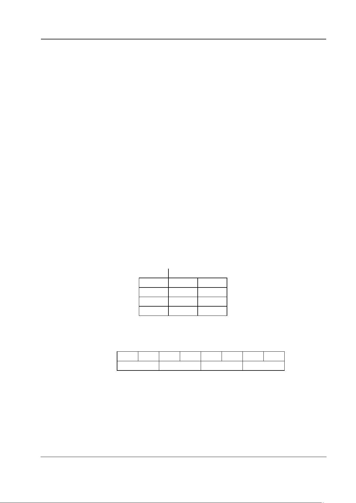
In transmit mode, the data symbols are passed through this filter to eliminate the high frequency components
that would otherwise cause interference into adjacent radio channels.
Data
encoding
binary symbol
Transmit
filter
Frequency
modulator
Binary
data
Modem
2 or 4-level
symbols
Filtered
baseband
signal
Figure 4: Generation of Filtered Tx Baseband Signal
In receive mode, the filter is used to reject HF noise and to equalize the received signal to a form suitable for
extracting the received data.
4.1.12 Tx Output Buffer
This is a unity gain amplifier used in transmit mode to buffer the output of the Tx low pass filter. In receive
mode, the input of this buffer is connected to V
BIAS
unless the RXEYE bit of the Control Register is '1', when it
is connected to the received signal. When changing from Rx to Tx mode the input to this buffer will be
connected to V
BIAS
for 8 symbol times in RD-LAP mode, 2 symbol times in MDC mode, while the low pass
filter settles.
Note: The RC low pass filter formed by the external components R4 and C5 between the TXOUT pin and the
input to the radio's frequency modulator forms an important part of the transmit out of band spurious signal
filtering. These components may form part of any dc level-shifting and gain adjustment circuitry. C5 should be
positioned to give maximum attenuation of high frequency noise into the modulator.
4.1.13 Clock Oscillator and Dividers
These circuits derive the transmit symbol rate (and the nominal receive symbol rate) by frequency division of
a reference frequency which may be generated by the on-chip Xtal oscillator or applied from an external
source.
Note: If the on-chip xtal oscillator is to be used, then the external components X1, C3, C4 and R3 are
required. If an external clock source is to be used, then it should be connected to the XTAL input pin, the
XTAL pin should be left unconnected, and X1, C3, C4 and R3 not fitted.
MOTIENTSM/ARDIS
SM
RD-LAP
TM
MDC4800 Modem 9 CMX969 Advance Information
¤¤¤¤2001 MX-COM, Inc. www.mxcom.com Tel: 800 638 5577 336 744 5050 Fax: 336 744 5054 Doc. # 20480211.002
4800 Bethania Station Road, Winston-Salem, NC 27105-1201 USA All trademarks and service marks are held by their respective companies.
4.2 Modem - µC Interaction
In general, data is transmitted over-air in the form of messages, or 'Frames', consisting of a 'Frame Preamble'
followed by one or more formatted data blocks. The Frame Preamble includes a Frame Synchronization
pattern designed to allow the receiving modem to identify the start of a frame. The following data blocks are
constructed from the 'raw' data using a combination of CRC (cyclic redundancy checksum) generation,
Forward Error Correction coding and Interleaving. Details of the message formats handled by the modem are
given in Section 4.4 and Figure 5 and Figure 6.
To reduce the processing load on the associated
µC, the CMX969 modem has been designed to perform as
much as possible of the computationally intensive work involved in Frame formatting and de-formatting and when in receive mode - in searching for and synchronizing onto the Frame Preamble. In normal operation the
modem will only require servicing by the µC once per received or transmitted block.
Thus, to transmit a block, the controlling µC has only to load the - unformatted - 'raw' binary data into the
modem's Data Block Buffer then instruct the modem to format and transmit that data. The modem will then
calculate and add the CRC bits as required, encode the result as 2 or 4-level symbols (with Forward Error
Correction coding) and interleave the symbols before transmission.
In receive mode, the modem can be instructed to assemble a block's worth of received symbols, de-interleave
the symbols, translate them to binary - using the FEC coding to correct as many errors as possible - and
check the resulting CRC before placing the received binary data into the Data Block Buffer for the µC to read.
The modem can also transmit and receive un-formatted data using the T4S, T24S, R4S, T8B, T40B and R8B
tasks described in Section 4.5.4. These are normally used for the transmission of Symbol and Frame
Synchronization sequences. They may also be used for the transmission and reception of special test
patterns.
4.3 Binary to RD-LAP 4-Level Symbol Translation
Although the over-air signal, and hence the signals at the modem TXOUT and RXIN pins, consists of 4-level
symbols in RD-LAP mode, the raw data passing between the modem and the µC is in binary form. Translation
between binary data and the 4-level symbols is done in one of two ways, depending on the task being
performed.
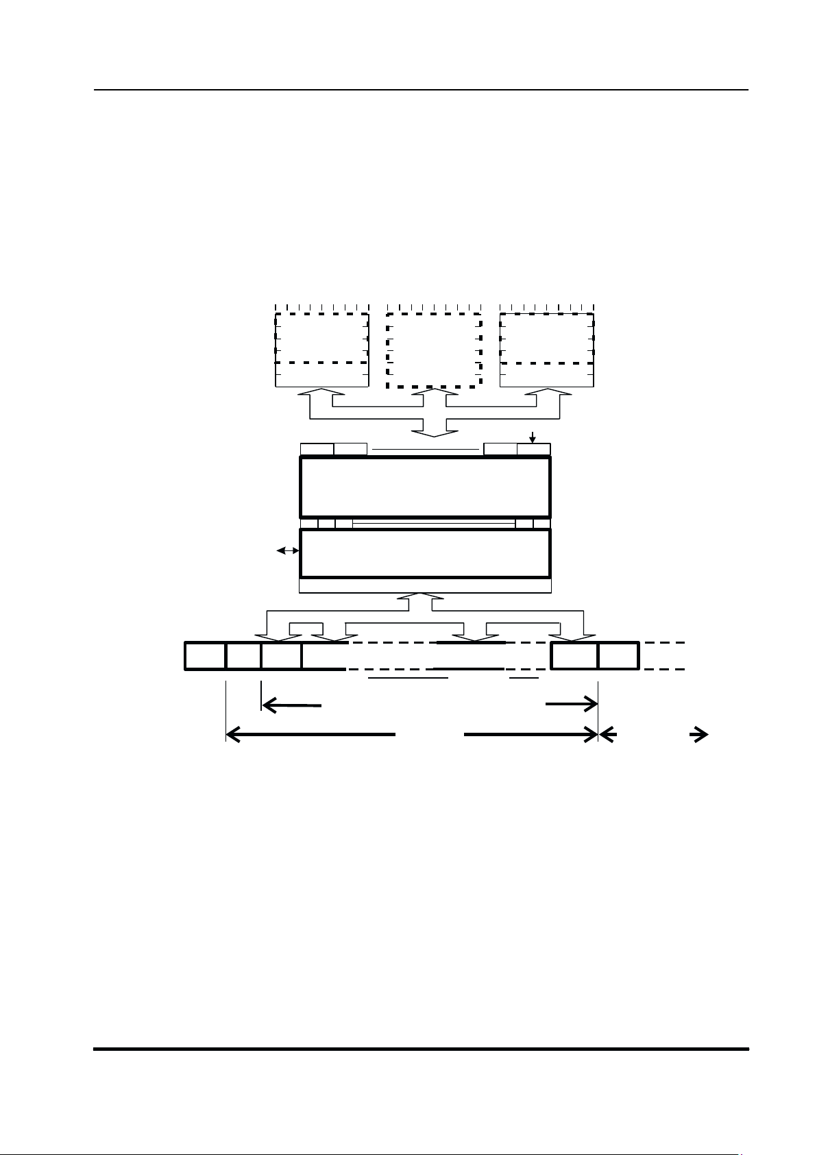
Direct: the simplest form, which converts between 2 binary bits and a single symbol, such as the 'S' Channel
Status symbol.
Symbol MSB LSB
+3 1 1
+1 1 0
-1 0 0
-3 0 1
This is expanded so that an 8-bit byte translates to four symbols for the T4S, T24S and R4S tasks described
in Section 4.5.2.
MSB LSB
Bits:
7 6 5 4 3 2 1 0
Symbols:
a b c d
sent first sent last
With FEC: This is more complicated, but essentially translates groups of 3 binary bits to pairs of 4-level
symbols using a Forward Error Correcting coding scheme for the block oriented tasks THB, TIB, TLB, TSID,
RHB, RILB and RSID described in Section 4.5.4.
MOTIENTSM/ARDIS
SM
RD-LAP
TM
MDC4800 Modem 10 CMX969 Advance Information
¤¤¤¤2001 MX-COM, Inc. www.mxcom.com Tel: 800 638 5577 336 744 5050 Fax: 336 744 5054 Doc. # 20480211.002
4800 Bethania Station Road, Winston-Salem, NC 27105-1201 USA All trademarks and service marks are held by their respective companies.
4.4 Frame Structure
In both RD-LAP and MDC modes the CMX969 performs all of the block formatting and de-formatting, the
binary data transferred between the modem and its
µC being that enclosed by the thick dashed rectangles
near the top of Figure 5 and Figure 6.
4.4.1 MDC Mode
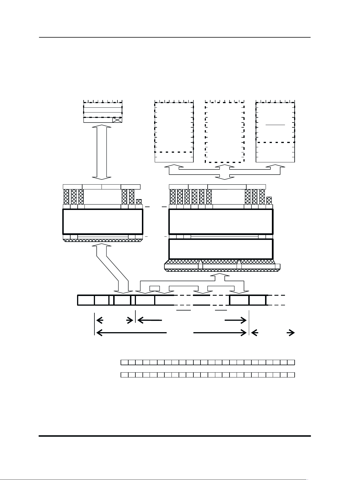
The CMX969 Frame Structure in MDC mode is illustrated in Figure 5, and consists of a Frame
Synchronization pattern followed by one or more 'Header’ blocks, one or more 'Intermediate’ blocks and a
'Last’ block. Channel Status bits are included at regular intervals. The first Frame of any transmission is
preceded by a Bit Synchronization pattern.
INTERLEAVING / DE-INTERLEAVING
FEC CODING / DECODING
(ERROR CORRECTION)
76543
Byte 0
Byte 1 Byte 5
21 0
Byte 4
Byte 5
Byte 0
Byte 1
Byte 2
Byte 3
Address
&
Control
(4 bytes)
CRC1
(2 bytes)
Header Block(s)
76543210
CRC2
(2 bytes)
Data and Pad bytes
(4)
Last Block
765432
00000000
10
Data Bytes
(6)
Intermediate Blocks
BIT
SYNC
FRAME
SYNC
FRAME
SYNC
PACKET (1 TO 46 BLOCKS)
FRAME
24 40
112 112 112 112
NEXT FRAME
(OPTIONAL)
Over-air
signal
(bits)
'LAST'
BLOCK
'HEADER'
BLOCK
INTERMEDIATE
BLOCKS
ADDITIONAL
HEADER BLOCKS
112 bits
Channel
Status bits
Figure 5: MDC Over Air Signal Format
MOTIENTSM/ARDIS
SM
RD-LAP
TM
MDC4800 Modem 11 CMX969 Advance Information
¤¤¤¤2001 MX-COM, Inc. www.mxcom.com Tel: 800 638 5577 336 744 5050 Fax: 336 744 5054 Doc. # 20480211.002
4800 Bethania Station Road, Winston-Salem, NC 27105-1201 USA All trademarks and service marks are held by their respective companies.
4.4.2 RD-LAP Mode
The CMX969 Frame Structure in RD-LAP mode is illustrated in Figure 6, and consists of a Frame Preamble
(comprising a 24-symbol Frame Synchronization pattern and Station ID block) followed by one or more
'Header’ blocks, one or more 'Intermediate’ blocks and a 'Last’ block. Channel Status (S) symbols are
included at regular intervals. The first Frame of any transmission is preceded by a Symbol Synchronization
pattern.
INTERLEAVING / DE-INTERLEAVING
76543210
Byte 4
Byte 5
Byte 6
Byte 7
Byte 8
Byte 9
Byte 0
Byte 1
Byte 2
Byte 3
Byte 10
Byte 11
Address
&
Control
(10 bytes)
CRC1
(2 bytes)
Header Block
76543210
CRC2
(4 bytes)
Pad bytes
(0 - 8)
Data bytes
(0 - 8)
Last Block
+3 +3 -3 -3 +3 +3 -3 -3 +3 +3 -3 -3 +3 +3 +3+3-3-3-3-3-3 -3 +3 +3
-1 +1 -1 +1 -1 +3 -3 +3 -3 -1 +1 -3 +3 +3 -1 +1 -3 -3 +1 +3 -1 -3 +1 +3
Frame Sync:
Symbol Sync:
sent first last
'S' : Channel Status Symbol : +3 = Busy +1 = Unknown -1 = Unknown -3 = Idle
76543210
Data Bytes
(12)
Intermediate Blocks
System ID
Domain ID
Base ID
CRC0
76543210
Byte 0
Byte 1
Byte 2
Byte 3
Station ID
msb lsb
FRAME
PREAMBLE
SYMBOL
SYNC
FRAME
SYNC
S
STATION
ID
S
FRAME
SYNC
PACKET (1 TO 44 BLOCKS)
FRAME
24 242211
69 69 6969
NEXT FRAME
(OPTIONAL)
Over-air
signal
(symbols)
'LAST'
BLOCK
'HEADER'
BLOCK
INTERMEDIATE BLOCKS
SS22 symbols 22 symbolsS 22 symbols
012 6465
012 3132
7070 70
Byte 0 Byte 1 Byte 11
'000'
34 5 2930
Block:
tri-bits
4-level
symbols
FEC TRELLIS CODING / DECODING
( ERROR CORRECTION )
12 9100
777000 0
8
'000'
0 1 20 21
7
2
Byte 0 Byte 1 Byte 2 Byte 3
FEC TRELLIS CODING / DECODING
( ERROR CORRECTION )
Figure 6: RD-LAP Over Air Signal Format
 Loading...