

MX COM Inc MX909ADS, MX909ADW, MX909ALH, MX919BDS, MX919BDW Datasheet
...
DATA BULLETIN
MX909A
GMSK MODEM DATA PUMP
1998 MX-COM, Inc. www.mxcom.com Tel: 800 638 5577 336 744 5050 Fax: 336 744 5054 Doc. # 20480134.003
4800 Bethania Station Road, Winston-Salem, NC 27105-1201 USA All trademarks and service marks are held by their respective companies.
PRELIMINARY INFORMATION
GMSK Modulation
Flexible Operating Modes
RX or TX up to 19.2k bits/sec
Host C Interface
Full Data Packet Framing
Low Power 3.3V/5.0V Operation
Mobitex Compatible
24-Pin Small Form Package Option
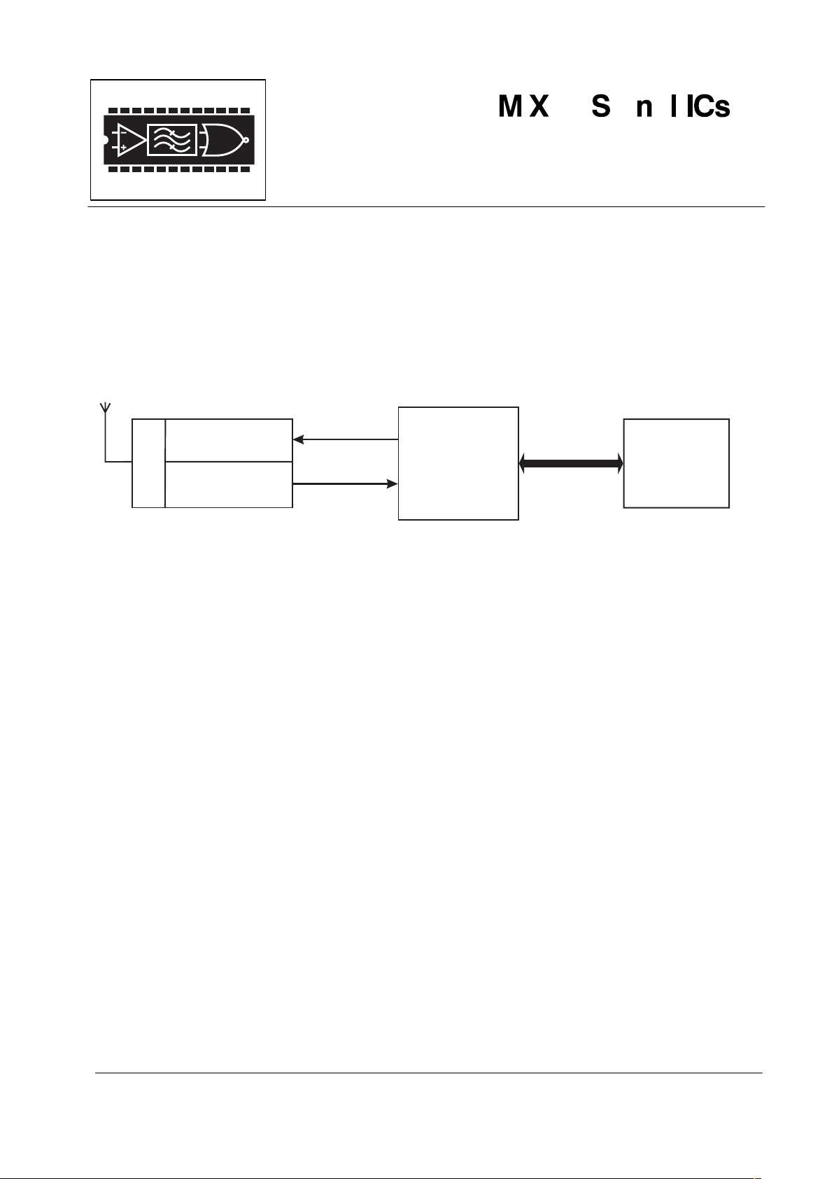
MODEM
DAT A
PUMP
MX909A
ANALOG TX
DATA AND
CONTROL BUS
ANALOG RX
RF
RADIO
DISCRIMINAT OR
MODULATOR
SYSTEM
APPLICATION
PROCESSING
HOST Cµ
The MX909A is a low power CMOS device containing all of the baseband signal processing and Medium
Access Control (MAC) protocol functions required for a high performance GMSK Wireless Packet Data
Modem. The MX909A interfaces with a host C and radio modulation/demodulation circuits to deliver reliable
two-way transfer of application data over a wireless link.
The MX909A assembles application data received from the host C, adds forward error correction (FEC), and
error detection (CRC) codes, time-spreads this data by interleaving (burst-error protection) and scrambles
(randomizes) the bit pattern. After automatically adding bit and frame sync codewords, the data packet is
converted into analog GMSK signals for modulating into the radio transmitter.
In the receive mode, the MX909A performs the reverse function using the analog signals from the receivers
discriminator. After error correction and removal of the packet overhead, the recovered application data is
supplied to the host C. Any CRC detected residual uncorrected errors in the data will be flagged. Readout
of the SNR value during receipt of a packet is also provided.
The MX909A uses data block sizes and FEC/CRC algorithms compatible with the Mobitex Wide Area
Network over-air standard. The format used is suitable for other private applications where the high-speed
transfer of data over narrow-band wireless links is required. The MX909A is programmable to operate at
standard bit-rates from a wide choice of XTAL/CLOCK frequencies.
The MX909A may be used with a 3.0V to 5.5V power supply and is available in the following packages:
24-pin SSOP (MX909ADS), 24-pin SOIC (MX909ADW), 24-pin PLCC (MX909ALH), and
24-pin PDIP (MX909AP).

GMSK Modem Data Pump 2 MX909A PRELIMINARY INFORMATION
1998 MX-COM, Inc. www.mxcom.com Tel: 800 638 5577 336 744 5050 Fax: 336 744 5054 Doc. # 20480134.003
4800 Bethania Station Road, Winston-Salem, NC 27105-1201 USA All trademarks and service marks are held by their respective companies.
CONTENTS
Section Page
1 Block Diagram................................................................................................................3
2 Signal List.......................................................................................................................4
3 External Components....................................................................................................5
4 General Description.......................................................................................................6
4.1 Description of Data Blocks................................................................................................ 6
4.2 Modem - µC Interaction.................................................................................................... 9
4.3 Data Formats.................................................................................................................... 9
4.4 The Programmer's View................................................................................................. 11
4.5 CRC, FEC, Interleaving and Scrambling Information..................................................... 22
5 Application ...................................................................................................................25
5.1 Transmit Frame Example ............................................................................................... 25
5.2 Receive Frame Example ................................................................................................ 27
5.3 Clock Extraction and Level Measurement Systems ....................................................... 29
5.4 AC Coupling ................................................................................................................... 30
5.5 Radio Performance......................................................................................................... 32
6 Performance Specification..........................................................................................33
6.1 Electrical Performance ................................................................................................... 33
6.2 Packaging....................................................................................................................... 37
MXCOM, Inc. Reserves the right to change specifications at any time and without notice.
GMSK Modem Data Pump 3 MX909A PRELIMINARY INFORMATION
1998 MX-COM, Inc. www.mxcom.com Tel: 800 638 5577 336 744 5050 Fax: 336 744 5054 Doc. # 20480134.003
4800 Bethania Station Road, Winston-Salem, NC 27105-1201 USA All trademarks and service marks are held by their respective companies.
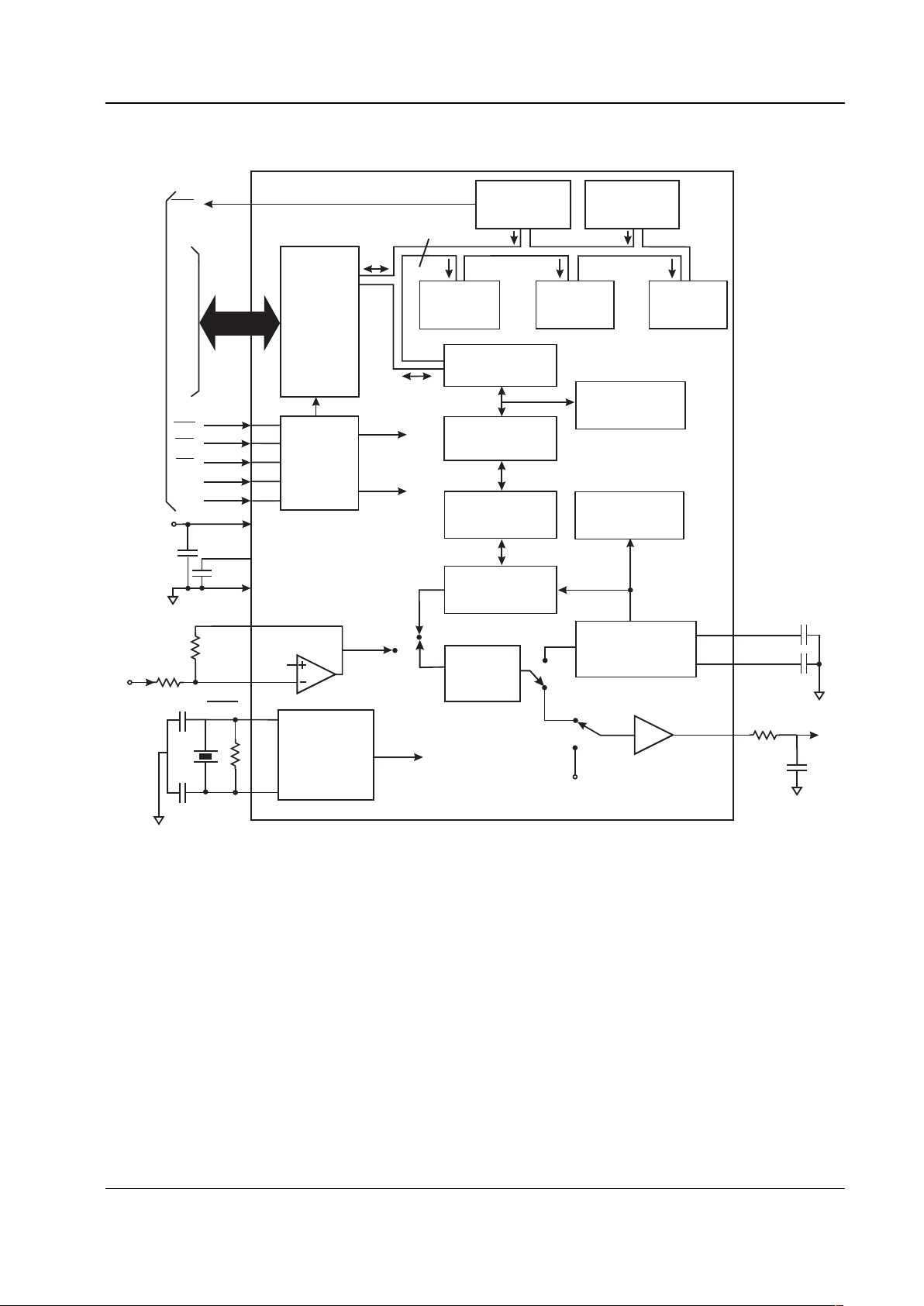
1 Block Diagram
V
SS
V
BIAS
XTAL /
CLOCK
TXOUT
RXIN
Rx Input Amp
Tx Output Buffer
DOC1
DOC2
D0
D1
D2
D3
D4
D5
D6
D7
A0
A1
8
Tx
Tx Bits
Rx Bits
Tx
Rx
Tx
Rx
Rx
V
BIAS
µCONTROLLER
INTERFACE
DATA
BUS
BUFFERS
ADDRESS
AND
R/W
DECODE
CRC
GENERATOR/
CHECKER
FRAME
SYNC DETECT
Rx LEVEL/CLOCK
EXTRACTION
FEC
GENERATOR/
CHECKER
INTERLEAVE/
DE-INTERLEAVE
SCRAMBLE/
DE-SCRAMBLE
CONTROL
REGISTER
MODE
REGISTER
COMMAND
REGISTER
DA T A
BUFFER
STA TUS
REGISTER
DATA
QUALITY
REGISTER
LOW PASS
FIL TER
CLOCK
OSCILLATOR
AND
DIVIDERS
RXAMPOUT
V
DD
XTAL
WR
RD
CS
IRQ
V
DD
V
BIAS
Figure 1: Block Diagram
GMSK Modem Data Pump 4 MX909A PRELIMINARY INFORMATION
1998 MX-COM, Inc. www.mxcom.com Tel: 800 638 5577 336 744 5050 Fax: 336 744 5054 Doc. # 20480134.003
4800 Bethania Station Road, Winston-Salem, NC 27105-1201 USA All trademarks and service marks are held by their respective companies.
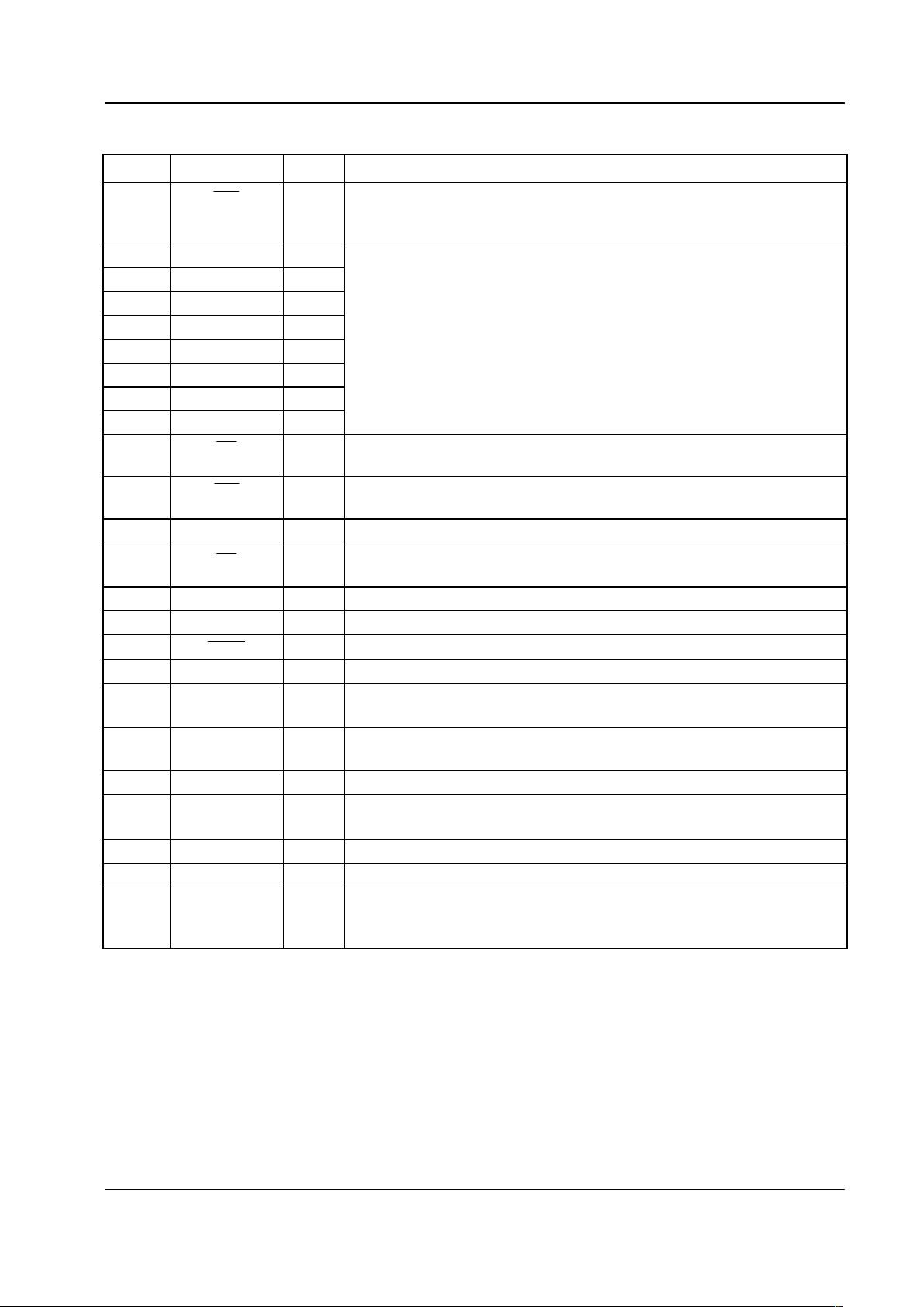
2 Signal List
Pin No Signal Type Description
1
IRQ
output
This pin is a ‘wire-ORable' output for connection to the host C's Interrupt
Request input. When active, this output has a low impedance pull down
to V
SS
. It has a high impedance when inactive.
2D7BUS
3D6BUS
4 D5 BUS Pins 2-9 (D7 - D0) are 8-bit, bi-directional, 3-state
5D4BUS
C interface data lines
6D3BUS
7D2BUS
8D1BUS
9D0BUS
10
RD
input Read. An active low logic level input used to control the reading of data
from the modem into the host C.
11
WR
input Write. An active low logic level input used to control the writing of data
into the modem from the host C.
12
V
SS
power Negative supply. (ground).
13
CS
input Chip Select. An active low logic level input to the modem. It is used to
enable a data read or write operation.
14 A0 input Logic level modem register select input.
15 A1 input Logic level modem register select input.
16
XTAL
output Output of the on-chip oscillator.
17 XTAL/CLOCK input Input to the on-chip oscillator, for an external CLOCK or XTAL circuit.
18 DOC 2 output Connects to the Rx level measurement circuitry. Should be capacitive
coupled to V
SS
.
19 DOC 1 output Connects to the Rx level measurement circuitry. Should be capacitive
coupled to V
SS.
20 TXOUT output Tx output signal from the modem.
21
V
BIAS
output
A bias line for the internal circuitry, held at V
DD
/2. This pin must be
bypassed to V
SS
by a capacitor mounted close to the device pins.
22 RXIN input Input to the Rx input amplifier.
23 RXAMPOUT output The output of the Rx input amplifier.
24
V
DD
power Positive supply. Voltage levels are dependent upon this supply. This pin
should be bypassed to V
SS
by a capacitor mounted close to the device
pins.
GMSK Modem Data Pump 5 MX909A PRELIMINARY INFORMATION
1998 MX-COM, Inc. www.mxcom.com Tel: 800 638 5577 336 744 5050 Fax: 336 744 5054 Doc. # 20480134.003
4800 Bethania Station Road, Winston-Salem, NC 27105-1201 USA All trademarks and service marks are held by their respective companies.
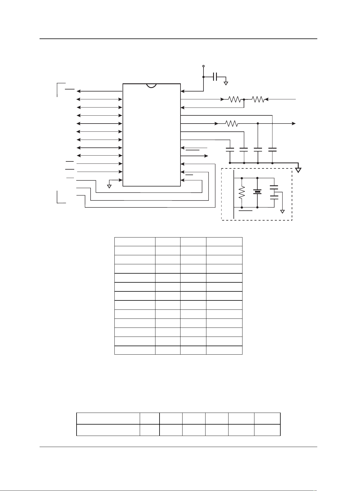
3 External Components
DOC1
DOC2
V
DD
V
DD
V
SS
V
BIAS
RXIN
GMSKIN
GMSKOUT
RXAMPOUT
R2
R4
R1
µCONTROLLER INTERFACE
MX909A
TXOUT
C7
C5
C3
C4
R3
X1
C6
C1
C2
D7
D6
D5
D4
D3
D2
D1
D0
A0
A1
A1
A0
XTAL/CLOCK
XTAL/CLOCK
1
2
3
4
5
6
8
9
10
11
12
13
14
7
24
23
22
21
20
19
18
17
17
16
16
15
IRQ
XT AL
XT AL
RD
WR
CS
CS
Figure 2: Recommended External Components
Component Notes Value Tolerance
R1 1
20%
R2
100k
10%
R3
1M
20%
R4 2
5%
C1 0.1 µF
20%
C2 0.1 µF
20%
C3 3
20%
C4 3
20%
C5 2
10%
C6 4
20%
C7 4
20%
X1 3
Recommended External Component Notes:
1. See section 4.1.10.
2. See section 4.1.12.
3. See section 4.4.3.
4. C6 and C7 values should satisfy the following formula:
C (Farads) = 120 x 10-6 / Data Rate (bits/second)
Data Rate (kbits/sec) 4.0 4.8 8.0 9.6 16.0 19.2
C6 / C7 (uF) 0.03 0.022 0.015 0.012 0.0068 0.0068
GMSK Modem Data Pump 6 MX909A PRELIMINARY INFORMATION
1998 MX-COM, Inc. www.mxcom.com Tel: 800 638 5577 336 744 5050 Fax: 336 744 5054 Doc. # 20480134.003
4800 Bethania Station Road, Winston-Salem, NC 27105-1201 USA All trademarks and service marks are held by their respective companies.
4 General Description
This product has been designed to be compliant with the appropriate sections of the “MobitexTM Interface
Specification”.
4.1 Description of Data Blocks
4.1.1 Data Bus Buffers
8 bi-directional, 3-state logic level buffers between the modem’s internal registers and the host C’s data bus
lines.
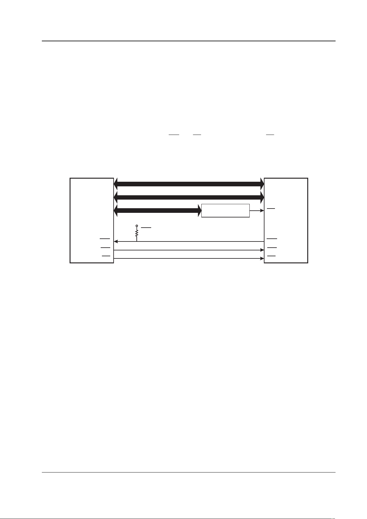
4.1.2 Address and R/W Decode
This block controls the transfer of data bytes between the C and the modem’s internal registers, according to
the state of the Write and Read Enable inputs (
WR and RD ), the Chip Select input CS), and the Register
Address inputs A0 and A1.
The Data Bus Buffers, Address, and R/W Decode blocks provide a byte-wide parallel C interface, which can
be memory mapped, as shown in Figure 3.
Address Bus
µC
MODEM
WR
RD
CS
RD
Address Decode
Circuit
Data Bus
IRQ
V
DD
D0:7
A0:1
WR
IRQ pull up
resistor
D0:7
IRQ
A2:7
A0:1
Figure 3: Typical Modem C Connections
4.1.3 Status and Data Quality Registers
8-bit registers which the µC can read to determine the status of the modem and the received data quality.
4.1.4 Command, Mode and Control Registers
The values written by the µC to these 8-bit registers control the operation of the modem.
4.1.5 Data Buffer
An 18-byte buffer used to hold receive or transmit data to or from the µC.
4.1.6 CRC Generator/Checker
A circuit which generates (in transmit mode) or checks (in receive mode) the Cyclic Redundancy Checksum
bits, which are included in transmitted Mobitex data blocks so the receive modem can detect transmission
errors.
4.1.7 FEC Generator/Checker
In transmit mode this circuit calculates and adds the Forward Error Correction (4 bits) to each byte presented
to it. In receive mode the FEC information is used to correct most transmission errors that have occurred in a
Mobitex Data Block or in the Frame Head control bytes.
4.1.8 Interleave / De-interleave Buffer
This circuit interleaves data bits within a data block before transmission and de-interleaves the received data
block so the FEC system is best able to handle short noise bursts or signal fades.
4.1.9 Frame Sync Detect
This circuit, (only active in receive mode), is used to look for the user specified 16-bit Frame Synchronization
pattern which is transmitted to mark the start of every frame.

GMSK Modem Data Pump 7 MX909A PRELIMINARY INFORMATION
1998 MX-COM, Inc. www.mxcom.com Tel: 800 638 5577 336 744 5050 Fax: 336 744 5054 Doc. # 20480134.003
4800 Bethania Station Road, Winston-Salem, NC 27105-1201 USA All trademarks and service marks are held by their respective companies.
4.1.10 Rx Input Amp
This amplifier allows the received signal input to the modem to be set to the optimum level by suitable
selection of the external components R1 and R2. The value of R1 should be calculated to give (0.2 x V
DD)VP-
P
at the RXAMPOUT pin for a received '...11110000...' sequence.
A capacitor may be fitted if AC coupling of the received signal is desired (see section 5.4), otherwise the DC
level of the received signal should be adjusted so that the signal at the modem's RXAMPOUT pin is centered
around V
BIAS
(VDD/2).
4.1.11 Tx/Rx Low Pass Filter
This filter, which is used in both transmit and receive modes, is a low pass transitional Gaussian filter having a
loss of 3dB at 0.3 times the selected bit rate (BT = 0.3). See Figure 4.
In transmit mode, the bits are passed through this filter to eliminate the high frequency components which
would otherwise cause interference into adjacent radio channels.
In receive mode this filter is used with an increased BT factor (0.56) to reject HF noise, so the signal is
suitable for extraction of the received data.
4.1.12 Tx Output Buffer
This is a unity gain amplifier used in transmit mode to buffer the output of the Tx low pass filter. In receive
mode, the input of this buffer is connected to V
BIAS
. When changing from Rx to Tx mode the input to this
buffer will be connected to V
BIAS
for 2 bit periods to prevent unwanted signals, from the low pass filter, at the
output. When the modem is set to powersave mode, the buffer is turned off and the TXOUT pin connected to
V
BIAS
via a high value resistance. When exiting from power save mode the Tx output is only reconnected to
the buffer after 2 bit periods, to prevent unwanted signals, from the low pass filter, at the output.
Note: The RC low pass filter formed by the external components R4 and C5 between the Tx Output Buffer
and the input to the radio's frequency modulator forms an important part of the transmit signal filtering.
These components may form part of any DC level-shifting and gain adjustment circuitry. The ground
connection to the capacitor C5 should be positioned to give maximum attenuation of high frequency
noise into the modulator. R4 and C5 should be chosen so that the product of the resistance of R4 and
capacitance of C5 is 0.34/bit rate (bit rate in bits per second). R4 should be not less than 47k and the
value used for the external capacitor should take into account parasitic capacitance.
Suitable values being:
R4 C5
8000 bits/sec 100k
430pF
4800 bits/sec
100k
710pF
The signal at the TXOUT pin is centered around V
BIAS
and is approx. (0.2 x VDD)V
P-P
, going positive for a
logic '1' and negative for a logic '0', if the modem is not inverting the Tx data.
A capacitor may be fitted if AC coupling of the input to the frequency modulator is desired, see section 5.4.
The 'eye' diagram of the transmitted signal (after the external R4/C5 network) is shown in Figure 5.

GMSK Modem Data Pump 8 MX909A PRELIMINARY INFORMATION
1998 MX-COM, Inc. www.mxcom.com Tel: 800 638 5577 336 744 5050 Fax: 336 744 5054 Doc. # 20480134.003
4800 Bethania Station Road, Winston-Salem, NC 27105-1201 USA All trademarks and service marks are held by their respective companies.
-80
-70
-60
-50
-40
-30
-20
-10
0
0 0.2 0.4 0.6 0.8 1 1.2 1.4 1.6 1.8 2
GAIN (dB)
FREQUENCY
DA T A RATE
Figure 4: Typical Tx Filter Frequency Response (after the external RC Filter)
012
Figure 5: Transmitted Eye Signal Diagram (after the external RC Filter)
4.1.13 Rx Level/Clock Extraction
These circuits, which operate only in receive mode, extract a bit rate clock from the received signal and
measure the received signal amplitude and DC offset. This information is then used to extract the received
bits and also to provide an input to the received Data Quality measuring circuit. The external capacitors C6
and C7 form part of the received signal level measuring circuit.

GMSK Modem Data Pump 9 MX909A PRELIMINARY INFORMATION
1998 MX-COM, Inc. www.mxcom.com Tel: 800 638 5577 336 744 5050 Fax: 336 744 5054 Doc. # 20480134.003
4800 Bethania Station Road, Winston-Salem, NC 27105-1201 USA All trademarks and service marks are held by their respective companies.
4.1.14 Clock Oscillator and Dividers
This circuit derives the transmit bit rate (and the nominal receive bit rate) by frequency division of a reference
frequency which may be generated by the on-chip Xtal oscillator or applied from an external source.
Note: If the on-chip Xtal oscillator is to be used, then external components X1, C3, C4 and R3 are required.
If an external clock source is to be used, then the external clock source should be connected to the
XTAL/CLOCK input pin, the
XTALpin should be left unconnected, and X1, C3, C4, and R3 not fitted.
4.1.15 Scramble/De-scramble
This block may be used to scramble/de-scramble the transmitted/received data blocks. It does this by
modulating the data with a 511-bit pseudorandom sequence, as described in section 4.5.4, smoothes the
transmitted spectrum, especially when repetitive sequences are to be transmitted.
4.2 Modem - µC Interaction
In general, data is transmitted over air in the form of messages, or 'Frames', consisting of a 'Frame Head'
optionally followed by one or more formatted data blocks. The Frame Head includes a Frame
Synchronization pattern designed to allow the receiving modem to identify the start of a frame. The following
data blocks are constructed from the 'raw' data using a combination of CRC (Cyclic Redundancy Checksum)
generation, Forward Error Correction coding, Interleaving and Scrambling. Details of the message formats
handled by this modem are given in section 4.3.
To reduce the processing load on the host µC, this modem has been designed to perform as much as
possible of the computationally intensive work involved in Frame formatting / de-formatting and (when in
receive mode) in searching for and synchronizing onto the Frame Head. In normal operation the modem will
only require servicing by the µC once per received or transmitted data block.
Thus, to transmit a block, the host µC has only to load the unformatted (raw) binary data into the modem's
data buffer then instruct the modem to format and transmit that data. The modem will then calculate and add
the CRC bits as required, encode the result with Forward Error Correction coding, interleave then scramble
the bits before transmission.
In receive mode, the modem can be instructed to assemble a block's worth of received bits, de-scramble and
de-interleave the bits, check and correct them (using the FEC coding) and check the resulting CRC before
placing the received binary data into the Data Buffer for the µC to read.
The modem can also handle the transmission and reception of unformatted data, to allow the transmission of
special Bit and Frame Synchronization sequences or test patterns.
4.3 Data Formats
4.3.1 General Purpose Formats
In a proprietary system the user may employ the data elements provided by this device to construct a custom,
over-air data structure.
For example, 16 bits of bit sync + 2 bytes of frame sync + 4 bytes of receiver and sender address + n data
blocks would be: transmitted as:
TQB (bit and frame sync) + TQB (addresses) + (n x TDB) + TSB
received as:
SFS + RSB + RSB + RSB + RSB + (n x RDB)
Note: It is important to have established frame Synchronization before receiving data to enable the receiving
device to decode synchronously. The user may add, by way of algorithms performed on the controlling
device, additional data correction with the bytes in the data block task.
4.3.2 Mobitex Frame Structure
The Mobitex format for transmitted data is in the form of a Frame Head immediately followed by a number of
Data Blocks (0 to 32).
The Frame Head consists of 7 bytes:
2 bytes of bit sync:
1100110011001100 from base,
0011001100110011 from mobile
bits are transmitted from left to right

GMSK Modem Data Pump 10 MX909A PRELIMINARY INFORMATION
1998 MX-COM, Inc. www.mxcom.com Tel: 800 638 5577 336 744 5050 Fax: 336 744 5054 Doc. # 20480134.003
4800 Bethania Station Road, Winston-Salem, NC 27105-1201 USA All trademarks and service marks are held by their respective companies.
Mobitex Frame Structure cont...
2 bytes of frame sync:
System specific.
2 bytes of control data.
1 byte of FEC code, 4 bits for each of the control bytes:
bits 7-4 (leftmost) operate on the first control byte.
bits 3-0 (rightmost) operate on the second control byte.
Each byte in the Frame Head is transmitted bit 7 (MSB) first to bit 0 (LSB) last.
The Data Block consists of:
18 bytes of data.
2 bytes of CRC calculated from the 18 data bytes.
4 bits of FEC code for each of the data and CRC bytes
The resulting 240 bits are interleaved and scrambled before transmission.
The over air signal is composed of Frame Sync and Bit Sync patterns, Control bytes, and Data Blocks as
shown in Figure 6.
The binary data transferred between the modem and the host µC is shown in the Frame Head and Data Block
of Figure 6 as shaded areas.
INTERLEAVING / DE-INTERLEAVING
SCRAMBLE / DESCRAMBLE
7654321
0
CRC (2 bytes)
loaded first
loaded last
4
5
6
7
8
9
0
1
2
3
18
19
14
15
16
17
10
11
12
13
FEC
LSB
MSB
321076543210
Frame H ead
MSB LSB
FEC2FEC1
Byte
loaded first
loaded last
1
2
4
3
5
6
Data Block
DB 0
DB n
DB 1
DB 2 DB 3 DB 4
FRAME
SYNC
16
16
8
FRAME HEAD
16
BITS
CTRL
BYTES
BIT
SYNC
FEC
DATA
BLOCKS
DAT A BLOCKS (0 to 32)
FRAME
OVER - AIR
SIGNAL
0
Byte
Data
(18 bytes)
Bit Sync 1
Bit Sync 2
Frame Sync 1
Frame Sync 2
Control Byte 1
Control Byte 2
Figure 6: Mobitex Over Air Signal Format
GMSK Modem Data Pump 11 MX909A PRELIMINARY INFORMATION
1998 MX-COM, Inc. www.mxcom.com Tel: 800 638 5577 336 744 5050 Fax: 336 744 5054 Doc. # 20480134.003
4800 Bethania Station Road, Winston-Salem, NC 27105-1201 USA All trademarks and service marks are held by their respective companies.
4.4 The Programmer's View
The modem appears to the programmer as 4 write only 8-bit registers shadowed by 3 read only registers,
individual registers being selected by the A0 and A1 chip inputs:
A1 A0 Write to Modem Read from Modem
0 0 Data Buffer Data Buffer
0 1 Command Register Status Register
1 0 Control Register Data Quality Register
1 1 Mode Register not used
4.4.1 Data Buffer
This is an 18-byte read/write buffer which is used to transfer data (as opposed to command, status, mode,
data quality and control information) between the modem and the host µC.
It appears to the µC as a single 8-bit register; the modem ensuring that sequential µC reads or writes to the
buffer are routed to the correct locations within the buffer.
The µC should only access this buffer when the Status Register BFREE (Buffer Free) bit is '1'.
The buffer should only be written to while in Tx mode and read from while in Rx mode (except when loading
Frame Sync detection bytes while in Rx mode).
4.4.2 Command Register
Writing to this register tells the modem to perform a specific action or actions, depending on the setting of the
TASK, AQLEV and AQBC bits.
76543210
Command Register
AQBC AQLEV
Reserved
set to '0 0 0'
TASK
When there is no action to perform and not 'powersaved', the modem will be in an 'idle' state. If the modem is
in transmit mode the input to the Tx filter will be connected to V
BIAS
. In receive mode the modem will
continue to measure the received data quality and extract bits from the received signal, supplying them to the
de-interleave buffer, otherwise the received data is ignored.
4.4.2.1 Command Register B7: AQBC - Acquire Bit Clock
This bit has no effect in transmit mode.
In receive mode, when a byte with AQBC bit set to '1' is written to the Command Register, and TASK is not
set to RESET, it initiates an automatic sequence designed to achieve bit timing Synchronization with the
received signal as quickly as possible. This involves setting the Phase Locked Loop of the received bit timing
extraction circuits to its widest bandwidth, then gradually reducing the bandwidth as timing Synchronization is
achieved, until the 'normal' value set by the PLLBW bits of the Control Register is reached.
Setting this bit to '0' (or changing it from '1' to '0') has no effect, however note that the acquisition sequence
will be re-started every time that a byte written to the Command Register has the AQBC bit set to '1'.
The AQBC bit will normally be set up to 12 bits before an SFS (Search for Frame Sync) or SFH (Search for
Frame Head) task, however it may also be used independently to re-establish clock Synchronization quickly
after a long fade. Alternatively, an SFS or SFH task may be written to the Command Register with the AQBC
bit '0' if it is known that clock Synchronization does not need to be re-established. More details of the bit clock
acquisition sequence are given in section 5.3.
4.4.2.2 Command Register B6: AQLEV - Acquire Receive Signal Levels
This bit has no effect in transmit mode.
In receive mode, when a byte with AQLEV bit set to '1' is written to the Command Register and TASK is not
set to RESET, it initiates an automatic sequence designed to measure the amplitude and DC offset of the
received signal as rapidly as possible. This sequence involves setting the measurement circuits to respond
quickly at first, then

GMSK Modem Data Pump 12 MX909A PRELIMINARY INFORMATION
1998 MX-COM, Inc. www.mxcom.com Tel: 800 638 5577 336 744 5050 Fax: 336 744 5054 Doc. # 20480134.003
4800 Bethania Station Road, Winston-Salem, NC 27105-1201 USA All trademarks and service marks are held by their respective companies.
Command Register B6: AQLEV - Acquire Receive Signal Levels (cont...)
gradually increasing their response time, thereby improving the measurement accuracy, until the 'normal'
value set by the LEVRES bits of the Control Register is reached.
Setting this bit to '0' (or changing it from '1' to '0') has no effect, however the acquisition sequence will be re-
started every time a byte written to the Command Register has the AQLEV bit set to '1'.
The AQLEV bit will normally be set up to 12 bits before an SFS (Search for Frame Sync) or SFH (Search for
Frame Head) task is initiated, however it may also be used independently to re-establish signal levels quickly
after a long fade. Alternatively, an SFS or SFH task may be written to the Command Register with the
AQLEV bit at '0' if it is known that there is no need to re-establish the received signal levels. Further
information of the level measurement acquisition sequence is provided in section 5.3.
The error rate is highest immediately after an AQBC and AQLEV sequence is triggered and rapidly reduces to
its static value soon after. These erroneous bits could incorrectly trigger the frame sync detection circuits. It
is suggested that an SFH or SFS task be set 12 bits after setting either of the AQLEV or AQBC sequences.
4.4.2.3 Command Register B5, B4, B3
These bits should be set to '0'.
4.4.2.4 Command Register B2, B1, B0: TASK - Task
Operations such as transmitting a data block are treated by the modem as 'tasks' and are initiated when the
µC writes a byte to the Command Register with the TASK bits set to anything other than the 'NULL' code.
The µC should not write a task (other than NULL or RESET) to the Command Register or write to or read
from the Data Buffer when the BFREE (Buffer Free) bit of the Status Register is '0'.
Different tasks apply in receive and transmit modes.
When the modem is in transmit mode, all tasks other than NULL, RESET and TSO instruct the modem to
transmit data from the Data Buffer, formatting it as required. For these tasks the µC should wait until the
BFREE (Buffer Free) bit of the Status Register is '1', before writing the data to the Data Buffer, then it should
write the desired task to the Command Register. If more than 1 byte needs to be written to the Data Buffer,
byte number 0 of the block should be written first.
Once the byte containing the desired task has been written to the Command Register, the modem will:
Set the BFREE (Buffer Free) bit of the Status Register to '0'.
Take the data from the Data Buffer as quickly as it can - transferring it to the Interleave Buffer for
eventual transmission. This operation will start immediately if the modem is 'idle' (i.e. not transmitting
data from a previous task), otherwise it will be delayed until there is sufficient room in the Interleave
Buffer.
Once all of the data has been transferred from the Data Buffer the modem will set the BFREE and
IRQ bits of the Status Register to '1', (causing the chip
IRQ
output to go low if the IRQEN bit of the
Mode Register has been set to '1') to tell the µC that it may write new data and the next task to the
modem.
In this way the µC can write a task and the associated data to the modem while the modem is still transmitting
the data from the previous task. See Figure 7.
When the modem is in receive mode, the µC should wait until the BFREE bit of the Status Register is '1', then
write the desired task to the Command Register.
Once the byte containing the desired task has been written to the Command Register, the modem will:
Set the BFREE bit of the Status Register to '0'.
Wait until enough received bits are in the De-interleave Buffer.
Decode them as needed, and transfer any resulting data to the Data Buffer
Then the modem will set the BFREE and IRQ bits of the Status Register to '1', (causing the
IRQ
output to go low if the IRQEN bit of the Mode Register has been set to '1') to tell the µC that it may
read from the Data Buffer and write the next task to the modem. If more than 1 byte is contained in
the Data Buffer, byte number '0' of the data will be read first.
In this way the µC can read data and write a new task to the modem while the received bits needed for this
new task are being stored in the De-interleave Buffer. See Figure 8.
The above is not true for loading the Frame Sync detection bytes (LFSB): the bytes to be compared with the
incoming data must be loaded prior to the task bits being written.
Detailed timings for the various tasks are given in Figure 9 and Figure 10.
 Loading...