

COMMUNICATION SEMICONDUCTORS
CMX860
DATA BULLETIN
Telephone Signaling
Transceiver
¤¤¤¤2000 MX-COM, Inc. www.mxcom.com tel: 800 638 5577 336 744 5050 fax: 336 744 5054 Doc. # 20480222.001
4800 Bethania Station Road, Winston-Salem, NC 27105-1201 USA All trademarks and service marks are held by their respective companies.
ADVANCE INFORMATION
Features Applications
• V.23 1200/75bps FSK Transmit and Receive
• DTMF/Tones Transmit and Receive
• Line & Telephone Complementary Drivers
• Call Progress Decoder
• CAS Tones Detection and Generation
• Simple ‘C-BUS’ Serial Interface
• Low Power Operation
• ‘Powersave’ Standby Mode
• Least Cost Routers
• Vending Machines
• Alarm Systems
• Home Management Systems
• Remote Meter Reading
• Internet Appliance Applications
• Cable TV Set-Top Boxes
• Advanced Feature Phones
'C-BUS'
SERIAL
INTERFACE
PHONE
LINE
CMX860
PHONE
INTERFACE
LINE
INTERFACE
HOST
µC
TX USART / FSK MODULATOR
& TONE / DTMF GENERATOR
RX USART / FSK RECEIVER
CALL PROGRESS, CAS &
ANSWER TONE DETECTOR
DTMF DECODER
RING DETECTOR
HOOK DETECTOR
RELAY DRIVER
The CMX860 is a flexible, low power Telephone Signaling Transceiver IC designed for use in a wide range of
line-powered telephone equipment.
The IC combines the functions of a DTMF encoder and decoder, V.23 modulator and demodulator plus call
progression circuitry with analog switching between line and phone interfaces. Ring detection, local phone offhook detection, and a relay for line hook-switch operation are also provided under the control of C-BUS. The
ring and hook detectors operate while the remainder of the IC is powersaved, generating an interrupt to wakeup the host
µC when further processing or signaling is required.
All on-chip functions and switching arrangements are controlled via a serial bus (C-BUS). The CMX860 is
designed to operate at 2.7V and utilizes MX-COM’s low power DTMF decoder and V.23 modem technology.
The CMX860 is available in 28-pin SSOP (CMX860D6) and 28-pin SOIC (CMX860D1) packages.

Telephone Signaling Transceiver 2 CMX860 Advance Information
¤¤¤¤2000 MX-COM, Inc. www.mxcom.com tel: 800 638 5577 336 744 5050 fax: 336 744 5054 Doc. # 20480222.001
4800 Bethania Station Road, Winston-Salem, NC 27105-1201 USA All trademarks and service marks are held by their respective companies.
CONTENTS
Section Page
1. Block Diagram............................................................................................................... 4
2. Signal List...................................................................................................................... 5
3. External Components ................................................................................................... 7
3.1 Ring Detector Interface.........................................................................................................9
3.2 Hook Detector Interface...................................................................................................... 10
3.3 Line Interface...................................................................................................................... 10
3.4 Phone Interface .................................................................................................................. 10
4. General Description .................................................................................................... 11
4.1 Tx USART ..........................................................................................................................11
4.2 FSK Modulator.................................................................................................................... 12
4.3 Tx Filter and Equalizer........................................................................................................ 12
4.4 DTMF/Tones Generator...................................................................................................... 12
4.5 Tx Level Control and Output Buffers ................................................................................... 12
4.6 DTMF Decoder and Tone Detectors ................................................................................... 12
4.7 Rx Modem Filter and Equalizer........................................................................................... 13
4.8 FSK Demodulator ............................................................................................................... 13
4.9 Rx Data Register and USART............................................................................................. 14
4.10 Rx Modem Pattern Detectors (and Descrambler)............................................................. 14
4.11 Analog Signal Routing ..................................................................................................... 15
4.12 C-BUS Interface............................................................................................................... 15
4.12.1 General Reset Command (no data) ($01) ............................................................................ 16
4.12.2 General Control Register: 16-bit write-only ($E0)................................................................. 17
4.12.3 Transmit Mode Register: 16-bit write-only ($E1) .................................................................. 18
4.12.4 Receive Mode Register: 16-bit write-only ($E2) ................................................................... 20
4.12.5 Tx Data Register: 8-bit write-only ($E3) ............................................................................... 21
4.12.6 Rx Data Register: 8-bit read-only ($E5) ............................................................................... 21
4.12.7 Analog Signal Path Register: 8-bit write-only ($EC)............................................................. 22
4.12.8 Status Register: 16-bit read-only ($E6) ................................................................................ 23
4.12.9 Programming Register
(includes generation & detection of CAS): 16-bit write-only ($E8) ....................................... 26
4.12.10 Other Registers..................................................................................................................... 28

Telephone Signaling Transceiver 3 CMX860 Advance Information
¤¤¤¤2000 MX-COM, Inc. www.mxcom.com tel: 800 638 5577 336 744 5050 fax: 336 744 5054 Doc. # 20480222.001
4800 Bethania Station Road, Winston-Salem, NC 27105-1201 USA All trademarks and service marks are held by their respective companies.
5. Application Notes........................................................................................................ 29
6. Performance Specification......................................................................................... 30
6.1 Electrical Performance........................................................................................................ 30
6.1.1 Absolute Maximum Ratings .................................................................................................. 30
6.1.2 Operating Limits.................................................................................................................... 30
6.1.3 Operating Characteristics ..................................................................................................... 31
6.1.4 Timing ................................................................................................................................... 35
6.2 Packages............................................................................................................................ 35
MX-COM, Inc. reserves the right to change specifications at any time and without notice.
Telephone Signaling Transceiver 4 CMX860 Advance Information
¤¤¤¤2000 MX-COM, Inc. www.mxcom.com tel: 800 638 5577 336 744 5050 fax: 336 744 5054 Doc. # 20480222.001
4800 Bethania Station Road, Winston-Salem, NC 27105-1201 USA All trademarks and service marks are held by their respective companies.
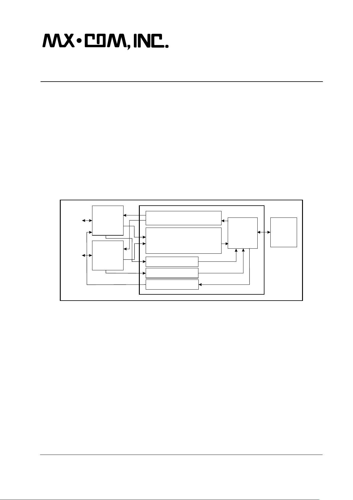
1. Block Diagram
CALL PROGRESS DECODER
DTMF DECODER
V.23 FSK DECODER
CAS DETECTOR
ANSWER TONE DETECTOR
DTMF/TONES GENERATOR
V.23 FSK GENERATOR
'C-BUS'
SERIAL
INTERFACE
SERIAL CLOCK
COMMAND DATA
REPLY DATA
CS
IRQ
V
BI AS
LINE
CONNECTION
PHONE
CONNECTION
RING
DETECT
OFF-HOOK
DETECT
XTAL
RDRV
XTAL/
CLOCK
RESET
DV
SS
AV
SS
DV
DD
AV
DD
EN
EN
LINE
RXAMPOUT
LINERX-
LINERX+
LINETX+
LINETX-
PHONE
RXAMPOUT
PHONERX-
PHONERX+
PHONETX+
PHONETX-
RT
RD
HT
HD
+
-
-
+
-
+
-
+
Figure 1: Block Diagram

Telephone Signaling Transceiver 5 CMX860 Advance Information
¤¤¤¤2000 MX-COM, Inc. www.mxcom.com tel: 800 638 5577 336 744 5050 fax: 336 744 5054 Doc. # 20480222.001
4800 Bethania Station Road, Winston-Salem, NC 27105-1201 USA All trademarks and service marks are held by their respective companies.
2. Signal List
CMX860
D6, D1
Signal
Pin No. Name Type
Description
1
XTAL
output The output of the on-chip Xtal oscillator inverter.
2 XTAL/CLOCK input The input to the oscillator inverter from the Xtal circuit or
external clock source.
3
RDRV
output Relay drive output, low resistance pull down to DV
SS
when active and medium resistance pull up to DV
DD
when inactive.
4 DVSS Power The digital negative supply rail (ground).
5 RD input Schmitt trigger input to the Ring signal detector. Connect
to DV
SS
if Ring Detector not used.
6 RT bi-directional Open drain output and Schmitt trigger input forming part
of the Ring signal detector. Connect to DV
DD
if Ring
Detector not used.
7
RESET
input An active-low reset pin. Can be used as part of a power-
up reset function.
8 LINE
RXAMPOUT
output The output of the Phone Rx Input Amplifier.
9 LINERX- input The inverting input to the Phone Rx Input Amplifier.
10 LINERX+ input The non-inverting input to the Phone Rx Input Amplifier.
11 PHONE
RXAMPOUT
output The output of the Line Rx Input Amplifier.
12 PHONERX- input The inverting input to the Line Rx Input Amplifier.
13 PHONERX+ input The non-inverting input to the Line Rx Input Amplifier.
14 AVSS Power The analog negative supply rail (ground).
15 V
BIAS
output Internally generated bias voltage of approximately
AV
DD
/2, except when the device is in ‘Powersave’ mode
when V
BIAS
will discharge to AVSS. Should be decoupled
to AV
SS
by a capacitor mounted close to the device pins.
16 PHONETX- output The inverted output of the Phone Tx Output Buffer.
17 PHONETX+ output The non-inverted output of the Phone Tx Output Buffer.
18 LINETX- output The inverted output of the Line Tx Output Buffer.
19 LINETX+ output The non-inverted output of the Line Tx Output Buffer.
20 AVDD Power The analog positive supply rail. Levels and thresholds
within the device are proportional to this voltage.
21 HT bi-directional Open drain output and Schmitt trigger input forming part
of the Hook signal detector. Connect to DV
DD
if Hook
Detector not used.
22 HD input Schmitt trigger input to the Hook signal detector.
Connect to DV
SS
if Hook Detector not used.
23
CS
input
The C-BUS chip select input from the
µC.
24 COMMAND DATA input
The C-BUS serial data input from the
µC.
25 SERIAL CLOCK input
The C-BUS serial clock input from the
µC.

Telephone Signaling Transceiver 6 CMX860 Advance Information
¤¤¤¤2000 MX-COM, Inc. www.mxcom.com tel: 800 638 5577 336 744 5050 fax: 336 744 5054 Doc. # 20480222.001
4800 Bethania Station Road, Winston-Salem, NC 27105-1201 USA All trademarks and service marks are held by their respective companies.
26 REPLY DATA tri-state
A 3-state C-BUS serial data output to the
µC. This output
is high impedance when not sending data to the
µC.
27
IRQ
output
A ‘wire-ORable’ output for connection to a
µC Interrupt
Request input. This output is pulled-down to DV
SS
when
active and is high impedance when inactive. An external
pull-up resistor is required i.e. R1 of Figure 2.
28 DVDD Power The digital positive supply rail. Levels and thresholds
within the device are proportional to this voltage.
The J5 package is only available as samples.
Table 1: Signal List
Telephone Signaling Transceiver 7 CMX860 Advance Information
¤¤¤¤2000 MX-COM, Inc. www.mxcom.com tel: 800 638 5577 336 744 5050 fax: 336 744 5054 Doc. # 20480222.001
4800 Bethania Station Road, Winston-Salem, NC 27105-1201 USA All trademarks and service marks are held by their respective companies.
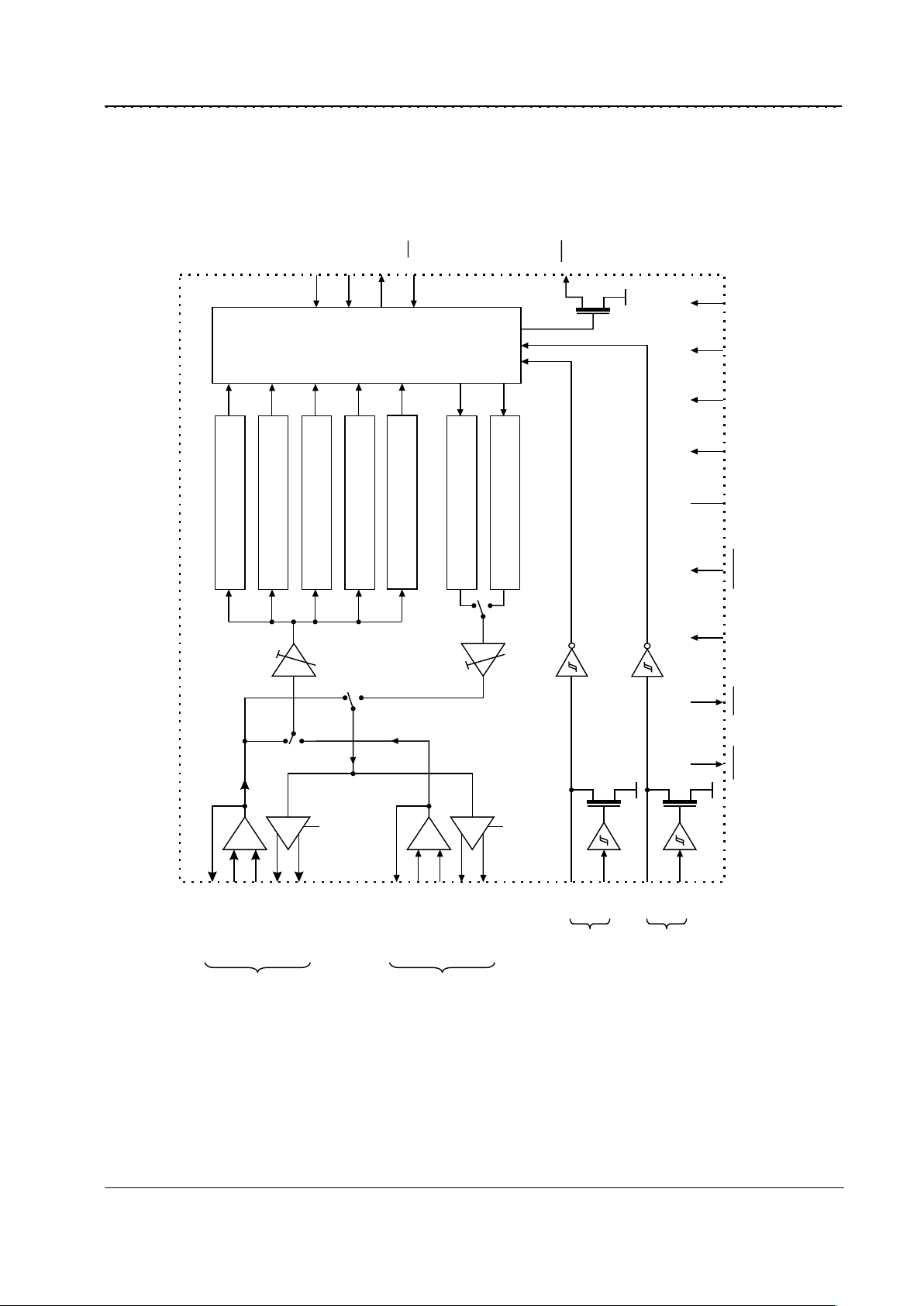
3. External Components
CMX860
D6/D1
1
C1
C2
C3
X1
XTAL
XTAL/CLOCK
'C-BUS'
to/from
µC
Ring
Detector
Hook
Detector
Phone
Interface
Line
Interface
Phone
Interface
Line
Interface
SERIAL CLOCK
COMMAND DATA
REPLY DATA
CS
HD
HT
IRQ
RDRV
RT
RESET
LINERXAMPOUT
LINERX+
LINERX-
PHONETX+
LINETX+
PHONERX-
PHONERXAMPOUT
PHONERX+
PHONETX-
LINETX-
RD
DV
DD
AV
SS
AV
SS
AV
SS
DV
SS
V
BI AS
2
5
6
8
9
10
11
7
12
13
14 15
16
17
18
19
20
21
22
23
24
25
26
27
28
R1
DV
DD
DV
DD
DV
SS
3
4
AV
DD
C6
C7
+
AV
DD
AV
SS
AV
SS
C4
C5
+
DV
DD
DV
SS
DV
SS
Figure 2: Recommended External Components for a Typical Application
R1
100k
Ω
C1, C2 22pF
X1 11.0592MHz C3, C4 100nF
or 12.288MHz C5 10uF
Resistors ±5%, capacitors ±20% unless otherwise stated.
Table 2: Recommended External Components for a Typical Application
This device is capable of detecting and decoding small amplitude signals. To achieve this DV
DD,
AV
DD,
and
V
BIAS
should be decoupled and the receive path protected from extraneous in-band signals. It is
recommended that the printed circuit board be laid out with both AV
SS
and DVSS ground planes in the
CMX860 area, as shown in Figure 3, with provision to make a link between them close to the CMX860. To
provide a low impedance connection to ground, the decoupling capacitors (C3-C7) must be mounted as close
to the CMX860 as possible and connected directly to their respective ground plane. This will be achieved
more easily by using surface mounted capacitors.
V
BIAS
is used as an internal reference for detecting and generating the various analog signals. It must be
carefully decoupled, to ensure its integrity. Apart from the decoupling capacitor shown (C3), no other loads
are allowed. If V
BIAS
needs to be used to set external analog levels, it must be buffered with a high input
impedance buffer. The DV
SS
connections to the Xtal oscillator capacitors C1 and C2 should also be of low
impedance and preferably be part of the DV
SS
ground plane to ensure reliable start up of the oscillator.

Telephone Signaling Transceiver 8 CMX860 Advance Information
¤¤¤¤2000 MX-COM, Inc. www.mxcom.com tel: 800 638 5577 336 744 5050 fax: 336 744 5054 Doc. # 20480222.001
4800 Bethania Station Road, Winston-Salem, NC 27105-1201 USA All trademarks and service marks are held by their respective companies.
CMX860
1
2
3
4
5
6
7
8
9
10
11
12
13
14
15
16
17
18
19
20
21
22
23
24
25
26
27
28
AV
SS
AV
SS
V
BI AS
DV
SS
Provision
for a
Wire Link
DV
SS
DV
DD
C3
C7
L2
L1
C6
C5
C4
DV
DD
AV
DD
AV
DD
+
+
Figure 3: Recommended Power Supply Connections and De-coupling
ANALOG DIGITAL
C3, C6 100nF C4 100nF
C7
10
µF
C5
10µF
L2 100nH L1 100nH
Note: Inductors L1 and L2 can be omitted but this may degrade system performance.
Table 3: Recommended Power Supply Connections and De-coupling
Telephone Signaling Transceiver 9 CMX860 Advance Information
¤¤¤¤2000 MX-COM, Inc. www.mxcom.com tel: 800 638 5577 336 744 5050 fax: 336 744 5054 Doc. # 20480222.001
4800 Bethania Station Road, Winston-Salem, NC 27105-1201 USA All trademarks and service marks are held by their respective companies.
3.1 Ring Detector Interface
Figure 4 shows how the CMX860 may be used to detect the large amplitude ringing signal voltage present on
the 2-wire line at the start of an incoming telephone call.
The ring signal is usually applied at the subscriber's exchange as an ac voltage inserted in series with one of
the telephone wires and will pass through either C20 and R20 or C21 and R21 to appear at the top end of
R22 (point X in Figure 4) in a rectified and attenuated form.
The signal at point X is further attenuated by the potential divider formed by R22 and R23 before being
applied to the CMX860 RD input. If the amplitude of the signal appearing at RD is greater than the input
threshold (Vt
HI
) of Schmitt trigger 'A' then the N transistor connected to RT will be turned on, pulling the
voltage at RT to DV
SS
by discharging the external capacitor C22. The output of the Schmitt trigger 'B' will then
go high, setting bit 14 (Ring Detect) of the Status Register.
The minimum amplitude ringing signal that is certain to be detected is:
( 0.7 + Vt
HI
x [R20 + R22 + R23] / R23 ) x 0.707V
RMS
where Vt
HI
is the high-going threshold voltage of the Schmitt trigger A (see Section 6.1).
With R20-22 all 470k
Ω as Figure 4, then setting R23 to 68kΩ will guarantee detection of ringing signals of
40Vrms and above for DV
DD
over the range 3V to 5V.
2-Wire
Telephone
Line
RD
CMX860
To Status
Register
RT
DV
DD
DV
SS
DV
SS
D1 - 4
C20
C22
R20
R21
R22
R23
R24
C21
RT
Status Register bit 14
(Ring Detect)
Bridge rectifier output (X)
Ring signal
Vt
HI
DV
SS
DV
SS
Vt
HI
A
B
X
Figure 4: Ring Signal Detector Interface Circuit
R20, 21, 22
470k
Ω
C20, 21
0.1µF
R23 See text C22
0.33
µF
R24
470k
Ω
D1-4 1N4004
Resistors ±5%, capacitors ±20%, unless otherwise stated
If the time constant of R24 and C22 is large enough then the voltage on RT will remain below the threshold of
the 'B' Schmitt trigger for the duration of a ring cycle.
The time for the voltage on RT to charge from DV
SS
towards DVDD can be derived from the formula:
V
RT
= DV
DD
x [1 - exp(-t/(R24 x C22)) ]
As the Schmitt trigger high-going input threshold voltage (Vt
HI
) has a minimum value of 0.56 x DVDD, then the
Schmitt trigger B output will remain high for a time of at least 0.821 x R24 x C22 following a pulse at RD.

Telephone Signaling Transceiver 10 CMX860 Advance Information
¤¤¤¤2000 MX-COM, Inc. www.mxcom.com tel: 800 638 5577 336 744 5050 fax: 336 744 5054 Doc. # 20480222.001
4800 Bethania Station Road, Winston-Salem, NC 27105-1201 USA All trademarks and service marks are held by their respective companies.
The values of R24 and C22 given in Figure 4 (470kΩ and 0.33µF) give a minimum RT charge time of 100ms,
which is adequate for ring frequencies of 10Hz or above.
Note, that the circuit will also respond to a telephone line voltage reversal. If necessary, the
µC can
distinguish between a Ring signal and a line voltage reversal by measuring the time that bit 14 of the Status
Register (Ring Detect) is high.
If the Ring detect function is not used then pin RD should be connected to DV
SS
and RT to DV
DD
.
3.2 Hook Detector Interface
This is identical internally to the Ring Detector interface circuit and similar components could be used
externally, with appropriate values, if hook detection is to be performed by detecting a voltage change across
the tip and ring lines to the local phone.
3.3 Line Interface
Figure 5: 2-Wire Line Interface Circuit: Application Circuits are TBD
3.4 Phone Interface
Figure 6: 2-Wire Phone Interface Circuit: Application Circuits are TBD
Telephone Signaling Transceiver 11 CMX860 Advance Information
¤¤¤¤2000 MX-COM, Inc. www.mxcom.com tel: 800 638 5577 336 744 5050 fax: 336 744 5054 Doc. # 20480222.001
4800 Bethania Station Road, Winston-Salem, NC 27105-1201 USA All trademarks and service marks are held by their respective companies.
4. General Description
The CMX860 transmit and receive operating modes are independently programmable.
The transmit mode can be set to any one of the following:
• V.23 modem. 1200 or 75bps FSK.
• DTMF transmit.
• Single tone transmit (from a range of modem calling, answer and other tone frequencies)
• User programmed tone or tone pair transmit (programmable frequencies and levels)
• Disabled.
The receive mode can be set to any one of the following:
• V.23 modem. 1200 or 75bps FSK.
• DTMF decode.
• 2100Hz and 2225Hz answer tone detect.
• Call progress signal detect.
• User programmed tone or tone pair detect.
• Disabled.
The CMX860 may also be set into a Powersave mode that disables all circuitry except for the C-BUS
interface, the Ring Detector and the Hook Detector.
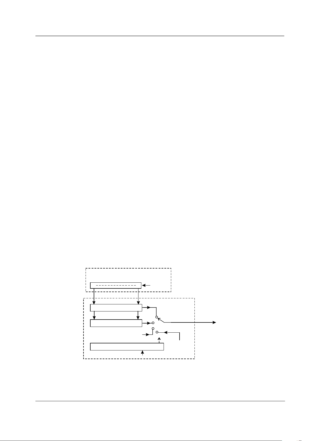
4.1 Tx USART
A flexible Tx USART is provided. It can be programmed to transmit continuous patterns, Start-Stop characters
or Synchronous Data.
In both Synchronous Data and Start-stop modes the data to be transmitted is written by the µC into the 8-bit
C-BUS Tx Data Register from which it is transferred to the Tx Data Buffer.
If Synchronous Data mode has been selected the 8 data bits in the Tx Data Buffer are transmitted serially, b0
being sent first.
In Start-stop mode a single Start bit is transmitted, followed by 5, 6, 7 or 8 data bits from the Tx Data Buffer b0 first - followed by an optional Parity bit then - normally - one or two Stop bits. The Start, Parity and Stop
bits are generated by the USART as determined by the Tx Mode Register settings and are not taken from the
Tx Data Register.
Tx Data Register
'C-BUS' Interface
Tx USART
Modem bit rate clock
Continuous
patterns
To FSK
Modulator
Tx data
from µC
Start/Stop
bits
Tx Data Buffer
Parity bit generator
USART Control
7 0
Figure 7: Tx USART
 Loading...