

DATA BULLETIN
Digitally Controlled
MX839
Analog I/O Processor
PRELIMINARY INFORMATION
Features Applications
x 4 input intelligent 10 bit A/D monitoring
subsystem
4 High and 4 Low Comparators
External IRQ Generator
Free Running Operation
x Three 8/10 bit DACs
x Two Variable Attenuators
x Selectable A/D Clock Frequencies
x Full Control via 4-wire Serial Interface
x Low Power 3.0 Operation
RECEIVER
RSSI VSWR
x PCS, Cellular, LMR, Wireless
Transceivers, and General Purpose
x Monitor and Control:
RSSI, Battery State, Temperature,
VSWR, and Error Voltages
x Digital Trim and Calibration:
VCOs, TCXO, Power Output, Bias,
Current, IF Gain, Deviation,
Modulation Depth, and Baseband
Gain
RF TRANSMITTER
RADIO
BATTERY
SYSTEM
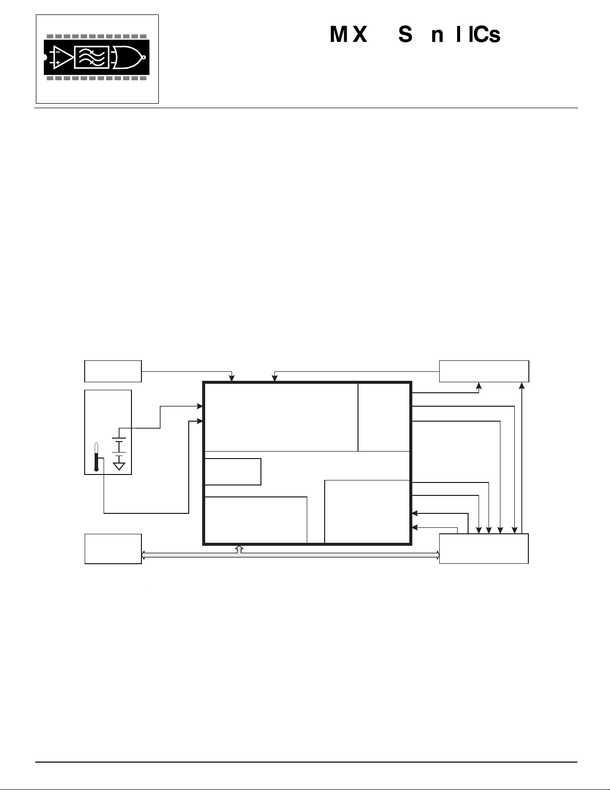
The MX839 is a low power CMOS µC peripheral device which provides digitally controlled calibration, trimming, and
monitoring functions for PCS, cellular, LMR, wireless transceivers, and general purpose applications.
Featuring a four input intelligent 10 bit A/D monitoring subsystem, an interrupt generator, three 8/10 bit DACs, and two
variable attenuator functions, the MX839 automatically monitors, produces, and trims up to nine analog signals via a
simple four wire serial control bus. The free running A/D intelligent monitoring subsystem includes independent high and
low limit comparators for each of four analog input signals which can be configured to generate external µC interrupts.
The MX839’s high level of integration reduces end product parts count, component size, and software complexity. MX839
digital trimming functions also reduce manufacturing costs by eliminating manual trimming operations.
Featuring an operating range of 3.0V to 5.5V the MX839 is available in 24-pin SSOP (MX839DS), 24-pin SOIC
(MX839DW), and 24-pin PDIP (MX839P) packages.
BATTERY STATE
TEMPERATURE
µC
C-BUS SERIAL BUS 0 : 3
4 x 10 bit Free Run A/D
4 x Hi Comparator
4 x Low Comparator
IRQ on Compare
Clock Osc
& Dividers
MX839
C-BU S In te rface
& Control Logic
3 x
8/10 bit
DAC
2 x
Variable
Attenuator
TX POWER
REF.OFFSET TRIM
VCO TRIM
MOD 1 OUT
MOD 2 OUT
MOD 1 IN
MOD 2 IN
TRANSMITTER
MODULATOR
© 1998 MXxCOM Inc. www.mxcom.com Tele: 800 638-5577 336 744-5050 Fax: 336 744-5054 Doc. # 20480164.002
4800 Bethania Station Road, Winston-Salem, NC 27105-1201 USA All trademarks and service marks are held by their respective companies.

Digitally Controlled Analog I/O Processor 2 MX839 PRELIMINARY INFORMATION
CONTENTS
Section Page
1 Block Diagram ................................................................................................................................ 3
2 Signal List ....................................................................................................................................... 4
3 External Components..................................................................................................................... 5
4 General Description ....................................................................................................................... 6
4.1 Variable Attenuators............................................................................................................................... 6
4.2 Digital to Analog Converters...................................................................................................................6
4.3 Analog to Digital Converter and A/D Clock Generator ........................................................................... 6
4.4 Magnitude Comparators and Interrupt Request..................................................................................... 7
4.5 Software Description .............................................................................................................................. 7
4.6 Read Only Registers (8-Bit and 16-Bit).................................................................................................. 9
4.7 Write Only Register Description ............................................................................................................. 9
4.8 Read Only Register Description............................................................................................................ 13
5 Application..................................................................................................................................... 13
5.1 C-Bus Clock .......................................................................................................................................... 13
6 Performance Specification ........................................................................................................... 14
6.1 Electrical Performance .......................................................................................................................... 14
6.2 Packaging.............................................................................................................................................. 19
MXxCOM, Inc. reserves the right to change specifications at any time and without notice.
© 1998 MXxCOM Inc. www.mxcom.com Tele: 800 638-5577 336 744-5050 Fax: 336 744-5054 Doc. # 20480164.002
4800 Bethania Station Road, Winston-Salem, NC 27105-1201 USA All trademarks and service marks are held by their respective companies.
Digitally Controlled Analog I/O Processor 3 MX839 PRELIMINARY INFORMATION
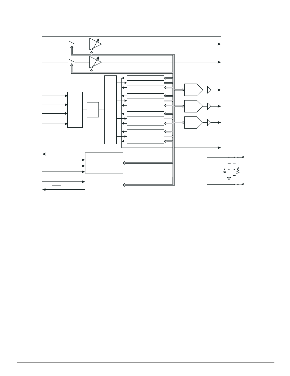
1 Block Diagram
MOD1 IN
MOD2 IN
MUTE1
MUTE2
A/DIN1
A/DIN2
4:1
A/DIN3
MUX
A/DIN4
REPLY DATA
COMMAND DATA
CS
SERIAL CLOCK
XTAL/CLOCK
XTAL
0 to 12dB x 0.4dB Steps
0 to 16dB x 0.2dB Steps
A/D
10
bit
1:4
MUX
4-wire
SERIAL INTERFACE
AND LOGIC
CONTROL
CLOCK
OSCILLATOR
AND DIVIDERS
HIGH COMPARATOR
A/D REG1
LOW COMPARATOR
HIGH COMPARATOR
A/D REG2
LOW COMPARATOR
HIGH COMPARATOR
A/D REG3
LOW COMPARATOR
HIGH COMPARATOR
A/D REG4
LOW COMPARATOR
MOD1OUT
MOD2OUT
DACOUT1
DAC1
8/10 bit
DACOUT2
DAC2
8/10 bit
DACOUT3
DAC3
8/10 bit
ADC COMP IRQ
AV
DD
V
SS
V
BIAS
DV
DD
AV
DV
DD
DD
Figure 1: Block Diagram
© 1998 MXxCOM Inc. www.mxcom.com Tele: 800 638-5577 336 744-5050 Fax: 336 744-5054 Doc. # 20480164.002
4800 Bethania Station Road, Winston-Salem, NC 27105-1201 USA All trademarks and service marks are held by their respective companies.
Digitally Controlled Analog I/O Processor 4 MX839 PRELIMINARY INFORMATION
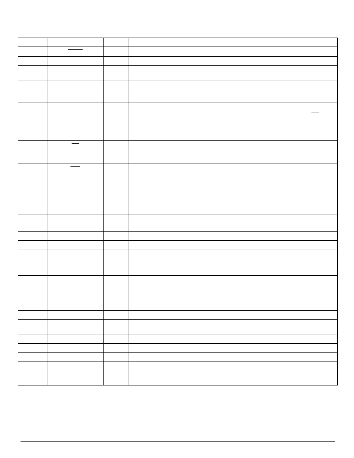
2 Signal List
Pin No. Name Type Description
1
XTAL
2 XTAL/CLOCK input The input to the on-chip oscillator inverter, for external Xtal circuit or clock.
3 SERIAL CLOCK input The 'C-BUS' serial clock input. This clock, produced by the µC, is used for
4 COMMAND DATA input The 'C-BUS' serial data input from the µC. Data is loaded into this device in
5 REPLY DATA output The 'C-BUS' serial data output to the µC. The transmission of REPLY DATA
6
7
CS
IRQ
8 A/DIN1 input Analog to digital converter input 1 (A/D1)
9 A/DIN2 input Analog to digital converter input 2 (A/D2)
10 A/DIN3 input Analog to digital converter input 3 (A/D3)
11 A/DIN4 input Analog to digital converter input 4 (A/D4)
12 V
13 V
SS
BIAS
14 N/C No internal connection. Do not make any connection to this pin.
15 DACOUT1 output Digital to analog converter No. 1 output (DAC1)
16 DACOUT2 output Digital to analog converter No. 2 output (DAC2)
17 DACOUT3 output Digital to analog converter No. 3 output (DAC3)
18 N/C No internal connection. Do not make any connection to this pin.
19 AV
DD
20 MOD1 IN input Input to MOD1 variable attenuator.
21 MOD2 IN input Input to MOD2 variable attenuator.
22 MOD1 output Output of MOD1 variable attenuator.
23 MOD2 output Output of MOD2 variable attenuator.
24 DV
DD
output The output of the on-chip oscillator inverter.
transfer timing of commands and data to and from the device. See Figure 5.
8-bit bytes, MSB (B7) first, and LSB (B0) last, synchronized to the SERIAL
CLOCK. See Figure 5.
bytes is synchronized to the SERIAL CLOCK under the control of the
CS
input.
This tri-state output is held at high impedance when not sending data to the
µC. See Figure 5.
input The 'C-BUS' data loading control function. This input is provided by the µC.
Data transfer sequences are initiated, completed or aborted by the
CS signal.
See Figure 5.
output This output indicates an interrupt condition to the µC by going to a logic '0'.
This is a 'wire-ORable' output, enabling the connection of up to 8 peripherals
to 1 interrupt port on the µC. This pin has a low impedance pulldown to logic
'0' when active and a high-impedance when inactive. An external pullup
resistor is required.
The conditions that cause interrupts are indicated in the IRQ FLAG register
and are effective if not disabled.
power Negative supply (ground) for both analog and digital supplies.
output An analog bias line for the internal circuitry, held at AVDD/2. This pin must be
bypassed by a capacitor mounted close to the device pins.
power Positive analog supply. Analog levels and voltages are dependent upon this
supply. This pin should be bypassed to V
by a capacitor.
SS
power Positive digital supply. Digital levels and voltages are dependent upon this
supply. This pin should be bypassed to V
by a capacitor.
SS
© 1998 MXxCOM Inc. www.mxcom.com Tele: 800 638-5577 336 744-5050 Fax: 336 744-5054 Doc. # 20480164.002
4800 Bethania Station Road, Winston-Salem, NC 27105-1201 USA All trademarks and service marks are held by their respective companies.
Digitally Controlled Analog I/O Processor 5 MX839 PRELIMINARY INFORMATION
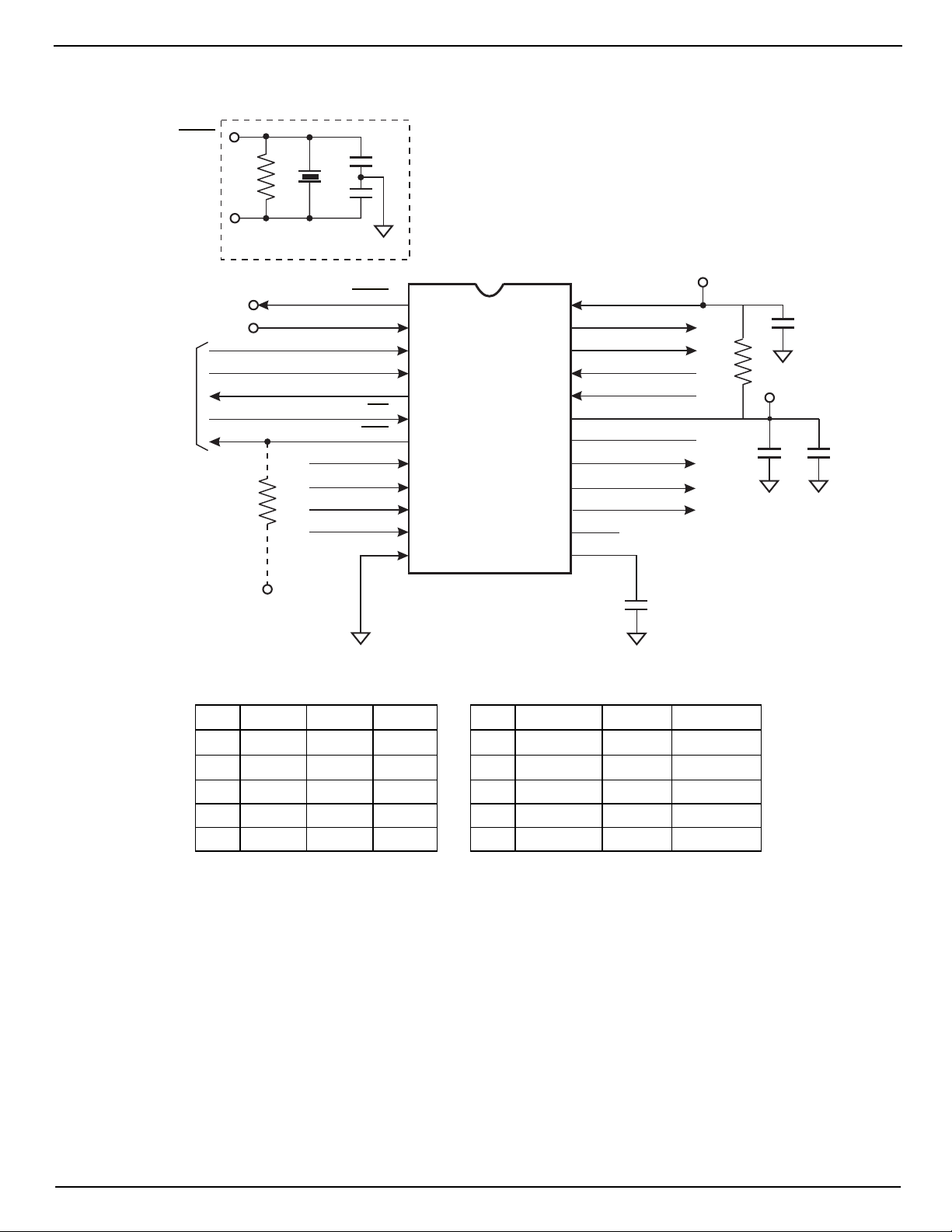
3 External Components
XTAL
X1
R1
XTAL/CLOCK
SERIAL CLOCK
COMMAND DATA
C-BUS
INTERFACE
R2
C2
C1
XTAL
XTAL/CLOCK
REPLY DATA
CS
IRQ
ADCIN1
ADCIN2
ADCIN3
ADCIN4
V
1
2
3
4
5
6
MX839
7
8
9
10
11
SS
12 13
24
23
22
21
20
19
18
17
16
15
14
DV
DD
MOD2 OUT
MOD1 OUT
MOD2 IN
MOD1 IN
AV
DD
N/C
DA COUT3
DA COUT2
DA COUT1
N/C
V
BIAS
DV
R3
DD
C5
AV
DD
C4
C6
DV
DD
C3
Figure 2: Recommended External Components
R1 1M
: ±5% C4 Note 1 0.1µF ±20%
R2 22k: ±10% C5 0.1µF ±20%
R3 Note 1 10: ±10% C6 Note 1 10.0µF ±20%
C1 22pF ±20%
C2 22pF ±20%
C3 0.1µF ±20% X1 Note 2, 3 ±100ppm
Table 1: Recommended External Components
Notes:
1. These values should be determined in regard to the amount of supply filtering required for D/A outputs.
2. If an external clock is to be used, then it should be connected to Pin 2 and the components C1, C2, R1, and X1
omitted. The ADC clock frequency is derived from the crystal or external clock by means of internal programmable
dividers. See Section 6 for details of crystal or external clock frequency range.
3. For best results, a crystal oscillator design should drive the clock inverter input with signal levels of at least 40% of
, peak to peak. Tuning fork crystals generally cannot meet this requirement. To obtain crystal oscillator design
V
DD
assistance, consult your crystal manufacturer.
© 1998 MXxCOM Inc. www.mxcom.com Tele: 800 638-5577 336 744-5050 Fax: 336 744-5054 Doc. # 20480164.002
4800 Bethania Station Road, Winston-Salem, NC 27105-1201 USA All trademarks and service marks are held by their respective companies.

Digitally Controlled Analog I/O Processor 6 MX839 PRELIMINARY INFORMATION
4 General Description
The device comprises four groups of related functions: variable attenuators, digital to analog converters, a multiplexed
analog to digital converter with multiplexer, clock generator and four 8-bit magnitude comparators with variable reference
levels. These functions are all controlled by the 'C-BUS' serial interface and are described below:
4.1 Variable Attenuators
The two variable attenuators have a range of 0 to -12dB and 0 to -6dB respectively and may be controlled independently.
4.2 Digital to Analog Converters
Three DACs are provided with default resolutions of 8 bits, which are defined at the initial chip reset. In this mode the
'C-BUS' data is transferred in a single byte. An option is provided to define any one or more of the DAC resolutions to be
10 bits, then the DAC requires the transfer of two 'C-BUS' data bytes.
The upper and lower DAC reference voltages are defined internally as AV
expressed as:
V
= AVDD x (DATA / 2n) [Volts]
OUT
Where, n is the DAC resolution (8 or 10 bits) and DATA is the decimal value of the input code. For example: n = 8 and
binary code = 11111111 therefore DATA = 255
V
= AVDD x (255 / 256) [Volts]
OUT
Any one of the three DAC input latches might be loaded by sending an address/command byte followed by one or two
data bytes to the 'C-BUS' interface. The data is then latched and the static voltage is updated at the appropriate output.
When a DAC is disabled, its output is defined as open-circuit.
and VSS respectively. The output voltage is
DD
4.3 Analog to Digital Converter and A/D Clock Generator
A single successive approximation A/D is provided with four multiplexed inputs. After a general reset command $01, the
A/D converter subsystem is disabled. To start conversions the Clock Control ($D0) and A/D control ($D7) registers must
be written (refer to Tables 2,6, and 8). Please note that A/D channel 1 must be active for any other channel to work. Also
note that A/D control register bit 5 (
conversions so the data being read does not change during the read which could otherwise result in erroneous data being
read. To re-enable conversions the A/D control register bit 5 (
The internal A/D clock frequency (f
control of this clock signal via the Clock Control Register ($D0), DIVIDER set per Table 6, and the choice of an external
system clock signal or a dedicated crystal. f
Since the typical application is for monitoring slowly changing control voltages, a Sample and Hold circuit is not included
at the input of the A/D. Thus, for the analog to digital conversion to be accurate, the input signal should not change
significantly during the conversion time. For ‘n-bit’ accuracy (with a maximum error of 1LSB) the maximum signal ‘linear
rate of change,’ ‘S,’ is defined by:
where: n is the number of bits of accuracy with a maximum error of 1 LSB
f
where:
A/D_CLK
XTAL
=f
DIVIDER
, DIVIDER is selected per Table 6.
For Example: The most significant bits (n) of accuracy.
For (n = 6) bit accuracy with AV
S = 9.77 [mV/PS]
For (n = 8) bit accuracy with AV
S = 1.95 [mV/PS]
For (n = 10) bit accuracy with AV
S = 0.27 [mV/PS]
The input signal should therefore be band limited to ensure the maximum signal ‘linear rate of change’ is not exceeded for
the desired accuracy.
READ) should be set low prior to issuing a ‘READ A/D DATA x’ command to disable
READ) bit must be set back high.
A/D_CLK
) is generated with a programmable clock generator. Users have flexible
A/D_CLK
should be chosen not to exceed 1MHz.
fAV
=S
n
=5V and f
DD
=5V and f
DD
=3.3V and f
DD
A/D_CLKDD
A/D_CLK
A/D_CLK
)2+n(10002
= 1MHz
= 1MHz
A/D_CLK
[mV/
= 1MHz
PS]
© 1998 MXxCOM Inc. www.mxcom.com Tele: 800 638-5577 336 744-5050 Fax: 336 744-5054 Doc. # 20480164.002
4800 Bethania Station Road, Winston-Salem, NC 27105-1201 USA All trademarks and service marks are held by their respective companies.
 Loading...