

MX COM Inc MX829DS, MX829DW, MX829P Datasheet
DATA BULLETIN
MX829
Baseband Signal Processor
© 1998 MX
•COM Inc. www.mxcom.com Tele: 800 638-5577 336 744-5050 Fax: 336 744-5054 Doc. # 20480160.004
4800 Bethania Station Road, Winston-Salem, NC 27105-1201 USA All trademarks and service marks are held by their respective companies.
PRELIMINARY INFORMATION
Features Applications
•
Rx Audio Processing
•
Tx Audio Processing
•
1200/2400 Baud Modem
•
DTMF Encoder
•
Low Voltage Operation
•
“C-BUS” Compatible
•
Host µC Interface
•
ETS/MPT/PAA Standards Compatible
•
LMR/PAMR/PMR Trunked Systems
•
Multi-standard Modem Formats
MX829
MSK MODEM
AUDIO PROCESSOR
DTMF ENCODER
LEVEL & VOLUME
CONTROLS
HOST µC
SERIAL BUS:
ANALOG Rx
Tx MOD 1
Tx MOD 2
RF
DISCRIMINAT OR
MODULA TOR
RADIO
DATA & CONTROL
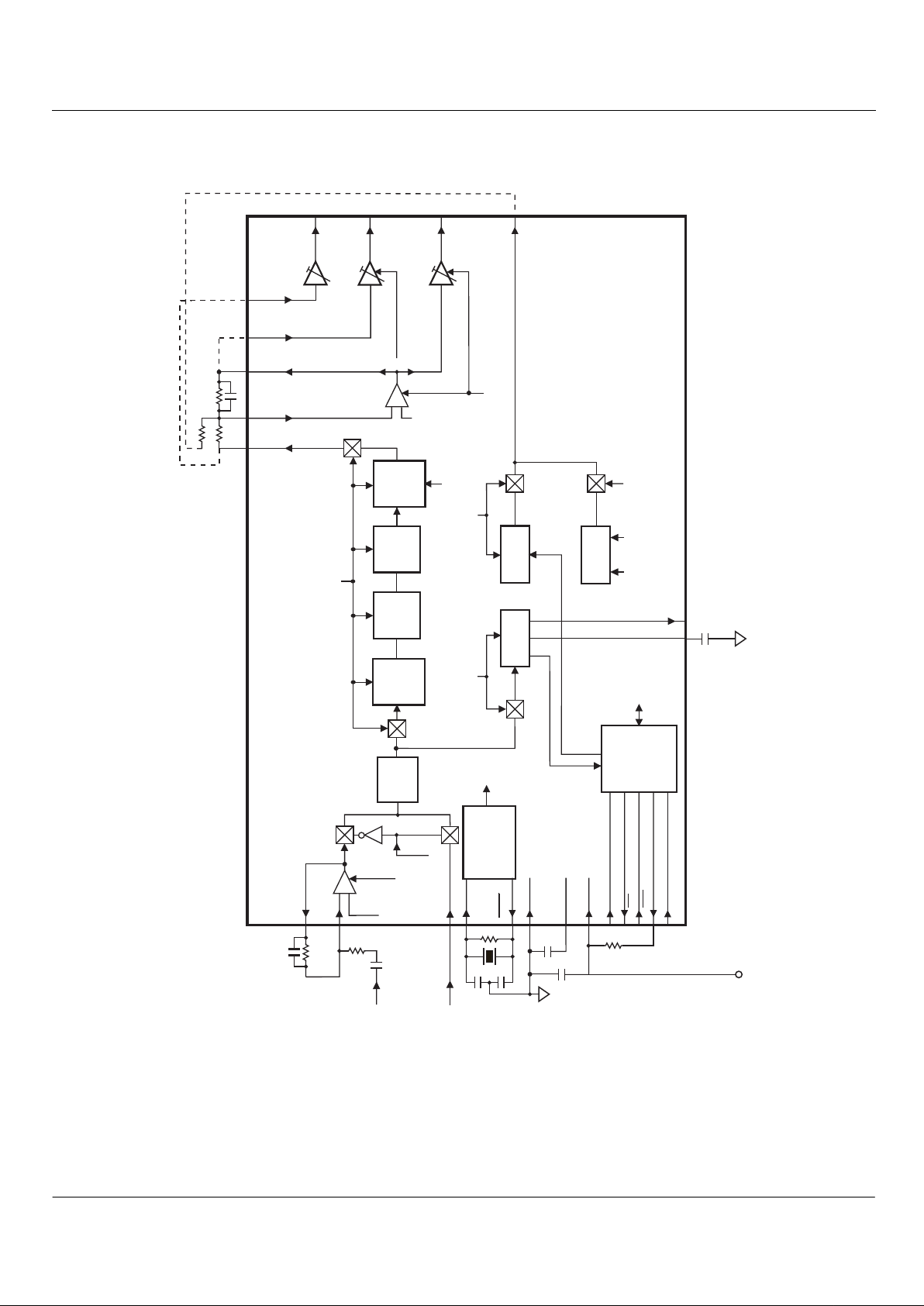
The MX829 is a low voltage CMOS integrated circuit, designed to provide baseband audio and system signal-processing
functions required for LMR/PAMR/PMR trunked radio applications. The MX829 operates in half-duplex mode under the
serial-bus control of a host µC.
The MX829 incorporates a dual-rate 1200/2400bps MSK modem, with a software-flexible choice of synchronization
codewords, data run-length and CRC checking to suit a wide range of applications. These features allow very flexible
handling of user defined data on traffic channels in addition to the network signaling sent on control channels. A 16
character DTMF encoder is available in the transmit mode. Software programmable output level-adjustment facilitates
two-point modulation circuits.
The audio processing stages include transmit and receive filtering (based on standards specified for 12.5kHz and 25kHz
LMR/PAMR/PMR channel operation), transmit deviation limiting, and a programmable Rx volume control. Power saving is
automatic when audio functions are disabled.
The MX829 is designed for use in radios compatible with MPT1327, PAA1382 and ETS 300 086 Trunking Standards.
The features and flexibility of the MX829 ensure that it is equally suitable for use with modified or proprietary standards.
The MX829 is available in the following packages: 24-pin SSOP (MX829DS), 24-pin SOIC (MX829DW), and
24-pin PDIP (MX829P).

Baseband Signal Processor 2 MX829 PRELIMINARY INFORMATION
© 1998 MX•COM Inc. www.mxcom.com Tele: 800 638-5577 336 744-5050 Fax: 336 744-5054 Doc. # 20480160.004
4800 Bethania Station Road, Winston-Salem, NC 27105-1201 USA All trademarks and service marks are held by their respective companies.
CONTENTS
Section Page
1. Block Diagram ................................................................................................................................ 3
2. Signal List ....................................................................................................................................... 4
3. External Components..................................................................................................................... 5
4. General Description ....................................................................................................................... 6
4.1 Audio Filtering........................................................................................................................................... 6
4.2 MOD1 and MOD2 Attenuators.................................................................................................................. 6
4.3 DTMF Encoder.......................................................................................................................................... 6
4.4 MSK Tx...................................................................................................................................................... 6
4.5 MSK Rx..................................................................................................................................................... 6
5. Software Description...................................................................................................................... 7
5.1 Address/Commands.................................................................................................................................. 7
5.2 Write Only Register Description................................................................................................................8
5.3 Read Only Register Description............................................................................................................... 14
5.4 MSK Checksum Generation and Checking..............................................................................................15
6. Application..................................................................................................................................... 17
6.1 Programming the MX829......................................................................................................................... 18
7. Performance Specification ........................................................................................................... 20
7.1 Electrical Performance............................................................................................................................. 20
7.2 Packaging................................................................................................................................................. 27
MX•COM, Inc. reserves the right to change specifications at any time and without notice
Baseband Signal Processor 3 MX829 PRELIMINARY INFORMATION
© 1998 MX•COM Inc. www.mxcom.com Tele: 800 638-5577 336 744-5050 Fax: 336 744-5054 Doc. # 20480160.004
4800 Bethania Station Road, Winston-Salem, NC 27105-1201 USA All trademarks and service marks are held by their respective companies.
1. Block Diagram
C-BUS
INTERFACE
AND
CONTROL
LOGIC
CLOCK
OSCILLATOR
AND
DIVIDERS
V
DD
V
BIAS
V
BIAS
V
BIAS
XT AL/
CLOCK
C1
C3
C6
C8
R2R6R3
R4
R5
C2
X1
R1
R7
MIC
DEMODIN
DEMODFB
DTMF
ENCODER
MSK Tx
SERIAL CLOCK
REPLY DATA
COMMAND DATA
MSK Rx ENABLE
AMP1
Input from
Demodulator
Input from
Mic. Amp.
MSK Tx ENABLE
DTMF
ENABLE
DTMFLO DTMFHI
CARDCAP
CARRIER
DETECT
BANDWIDTH
AUDIO ENABLE
LIMITER
TRIM
AMP2
TRIM
VOL
VOLUME
IN
AMP2
ENABLE
MOD1
ENABLE
AUDIO
LOW
P ASS
FILTER
AUDIO
LOW
P ASS
FILTER
SUM
OUT
MOD1
IN
SUM
IN
MOD1
MOD2
AUDIO
OUT
MSK/DTMF
OUT
ANTI-
ALIAS
FILTER
-
-
+
+
FILTER
OUT
HIGH
P ASS
FILTER
MIC/DEMODIN
AMP1
ENABLE
MSK Rx
C5
C7
C4
XT AL
CS
IRQ
V
SS
V
DD
Figure 1: Block Diagram

Baseband Signal Processor 4 MX829 PRELIMINARY INFORMATION
© 1998 MX•COM Inc. www.mxcom.com Tele: 800 638-5577 336 744-5050 Fax: 336 744-5054 Doc. # 20480160.004
4800 Bethania Station Road, Winston-Salem, NC 27105-1201 USA All trademarks and service marks are held by their respective companies.
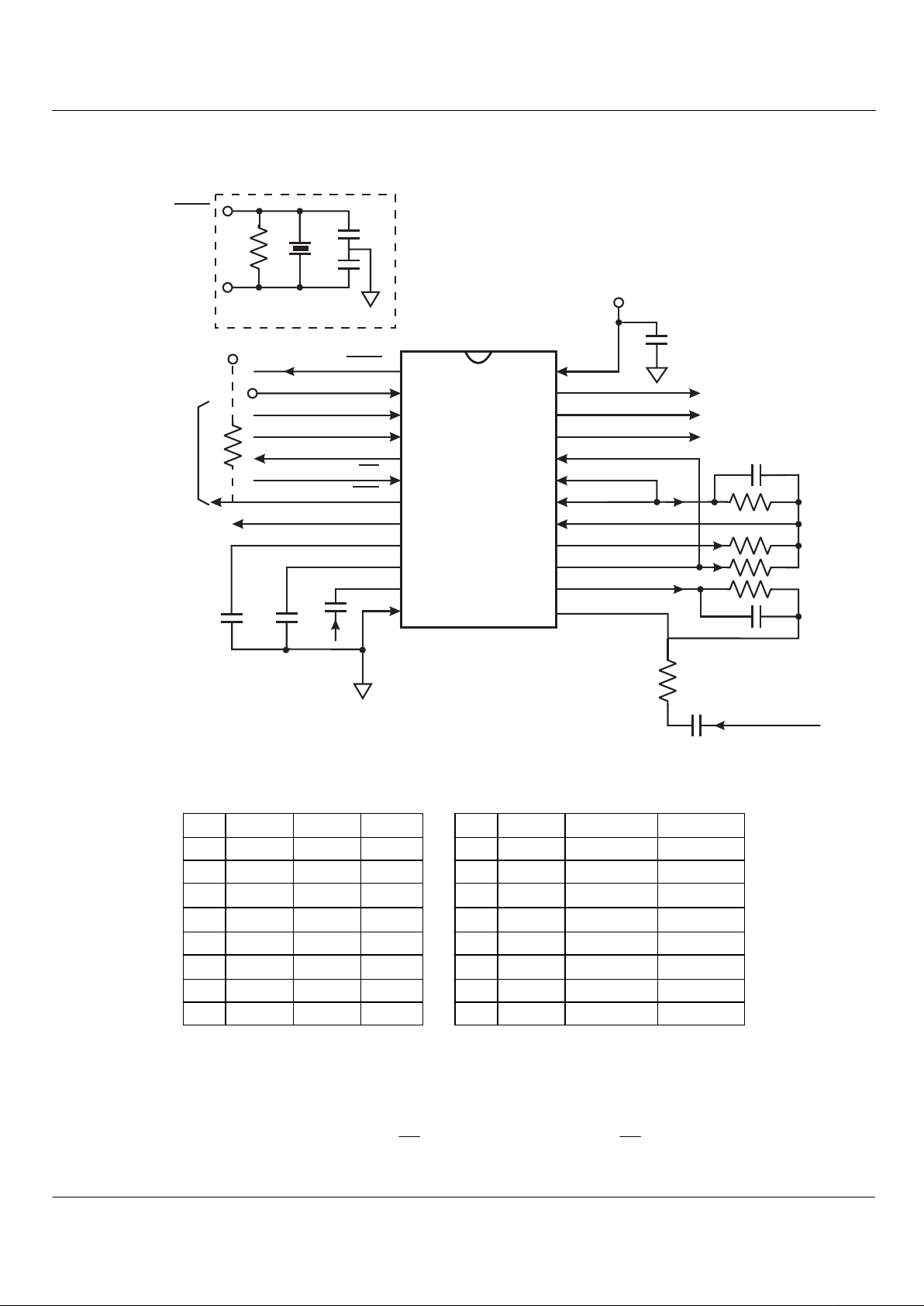
2. Signal List
PIN NO SIGNAL TYPE DESCRIPTION
1
XTAL
output Inverted output of the on-chip oscillator.
2 XTAL/CLOCK input Input to the on-chip oscillator, for external Xtal circuit or clock.
3 SERIAL CLOCK input "C-BUS" serial clock input. This clock, produced by the µController, is used for
transfer timing of commands and data to and from the device. See section
7.1.4
4 COMMAND DATA input "C-BUS" serial data input from the µController. Data is loaded into this device
in 8-bit bytes, MSB (B7) first, and LSB (B0) last, synchronized to the SERIAL
CLOCK. See section 7.1.4.
5 REPLY DATA output "C-BUS" serial data output to the µController. The transmission of REPLY
DATA bytes is synchronized to the SERIAL CLOCK under the control of the
CS
input. This 3-state output is held at high impedance when not sending
data to the µController. See section 7.1.4.
6
CS
input "C-BUS" data loading control function: this input is provided by the µController.
Data transfer sequences are initiated, completed or aborted by the
CS
signal.
See section 7.1.4.
7
IRQ
output This output indicates an interrupt condition to the µController by going to a
logic "0". This is a "wire-ORable" output, enabling the connection of up to 8
peripherals to 1 interrupt port on the µController. This pin has a low
impedance pulldown to logic "0" when active and a high-impedance when
inactive. An external pull-up resistor is required. The conditions that cause
interrupts are indicated in the STATUS register and are effective if not masked
out by a corresponding bit in the CONTROL register. The reading of the
Status Register resets the IRQ to a high impedance and sets the contents of
the Status Register to 0.
8 CARRIER DETECT output The carrier detect output for the MSK Rx.
9 CD CAP output The carrier detect integrating capacitor.
10 V
BIAS
output A bias line for the internal circuitry, held at VDD/2. This pin must be bypassed
to a capacitor mounted close to the device pins.
11 MIC input AC coupled Tx audio input (external amplification is required for use as a
microphone input).
12 V
SS
Power Negative supply (ground).
13 DEMOD IN input AC coupled inverting input to the Rx input amplifier (AMP1).
14 DEMOD FB output Output of the Rx input amplifier (AMP1)
15 FILTER OUT output Output of the audio filter/limiter section. In powersave mode this output is
connected to V
BIAS
via a 500kΩ resistor.
16 MSK/DTMF OUT output The 1200 or 2400 baud MSK Tx output and the DTMF encoder output. When
enabled but not transmitting MSK or DTMF signals, or when in powersave
mode, this output is connected to V
BIAS
via a 500kΩ resistor. On power-up,
this output can be any level: a General Reset command is required to ensure
that this output attains V
BIAS
initially.
17 SUM IN input Input to the audio summing amplifier (AMP2).
18 SUM OUT output Output of the audio summing amplifier (AMP2).
19 MOD1 IN input Input to MOD1 audio gain control.
20 VOL IN input Input to the audio volume control.
21 AUDIO OUT output Output of the audio volume control.
22 MOD1 output Output of MOD1 audio gain control.
23 MOD2 output Output of MOD2 audio gain control.
24 V
DD
Power Positive supply. Levels and voltages are dependent upon this supply. This pin
should be bypassed to V
SS
by a capacitor.
Baseband Signal Processor 5 MX829 PRELIMINARY INFORMATION
© 1998 MX•COM Inc. www.mxcom.com Tele: 800 638-5577 336 744-5050 Fax: 336 744-5054 Doc. # 20480160.004
4800 Bethania Station Road, Winston-Salem, NC 27105-1201 USA All trademarks and service marks are held by their respective companies.
3. External Components
MOD1 IN
SUM OUT
V
DD
V
DD
V
SS
V
BIAS
MOD1
AUDIO OUT
MOD2
SERIAL CLOCK
"C-BUS"
INTERFACE
COMMAND DATA
XTAL/CLOCK
MIC
DEMOD IN
R4
R2
R3
R5
R6
R7
Input from
Demodulator
MX829
VOL IN
C4
Mic
Input
C5
C3
C6
C8
C9
C7
REPLY DATA
CARRIER DETECT
CD CAP
DEMOD FB
FILTER OUT
SUM IN
MSK/DTMF OUT
1
2
3
4
5
6
8
9
10
11
12
13
14
7
24
23
22
21
20
19
18
17
16
15
XTAL/CLOCK
C1
C2
X1
R1
XTAL
XTAL
CS
IRQ
V
DD
Figure 2: Recommended External Components
C1 22pF ±20% R1
1M
Ω
±5%
C2 22pF ±20% R2 Note 1 ±10%
C3 68pF ±20% R3 Note 1 ±10%
C4 0.1µF ±20% R4
100k
Ω
±10%
C5 0.1µF ±10% R5
100k
Ω
±10%
C6 100pF ±20% R6 Note 2 ±10%
C7 0.1µF ±20% R7
22k
Ω
±10%
C8 Note 2 ±20%
C9 5.6nF ±20% X1 Note 3 4.032MHz ±100ppm
External Component Notes:
1. R2, R3, R4 and C3 form the gain components for the Summing Amplifier (AMP2).
R2 and R3 should be chosen as required from the system specification, using the following formula:
Audio Gain = -
R4
R3
DTMF Gain = -
R4
R2

Baseband Signal Processor 6 MX829 PRELIMINARY INFORMATION
© 1998 MX•COM Inc. www.mxcom.com Tele: 800 638-5577 336 744-5050 Fax: 336 744-5054 Doc. # 20480160.004
4800 Bethania Station Road, Winston-Salem, NC 27105-1201 USA All trademarks and service marks are held by their respective companies.
2. R5, R6, C6 and C8 form the gain components for the Rx Input Amplifier (AMP1).
R6 should be chosen as required by the signal level, using the following formula:
Gain = -
R5
R6
C8 x R6 should be chosen so as not to compromise the low frequency performance of this product.
3. For best results, a crystal oscillator design should drive the clock inverter input with signal levels of at least 40% of
VDD, peak to peak. Tuning fork crystals generally cannot meet this requirement. To obtain crystal oscillator design
assistance, consult your crystal manufacturer.
4. General Description
The MX829 consists of five main sections: the Audio Filter, the Programmable Attenuators, the DTMF encoder, the MSK
transmitter, and the MSK receiver. These sections are controlled via a serial ("C-BUS") interface. The five sections are
described below.
4.1 Audio Filtering
This consists of an input amplifier and a common audio filter section, which may be switched between Rx and Tx. The
filter section comprises an anti-alias filter followed by low-pass and high-pass filtering with an amplitude limiter to set the
maximum deviation. Three variable attenuation blocks may be used to set the volume (in Rx) or the modulation level (in
Tx). Pre- and de-emphasis can be added externally using resistors and capacitors around AMP1, AMP2 and the
microphone amplifiers, see Figure 7,Figure 8, and Figure 9. The anti-alias filter is designed to reduce aliasing effects
above 50kHz which is approximately half the internal filter's sample rate.
The filtering is designed to meet the ETS 300 086 specification.
Various powersave modes are incorporated.
4.2 MOD1 and MOD2 Attenuators
The MOD1 input can be connected directly to SUM OUT, so that the MOD1 and MOD2 outputs can then be used for two
point modulation. Alternatively, the MOD1 attenuator can be used for auxiliary gain adjustment, in which case the input
signal must be ac coupled with a suitable capacitor.
4.3 DTMF Encoder
This generates the standard DTMF tones according to the CONTROL 2 Register settings. It also has a powersave mode.
4.4 MSK Tx
The Tx function of the MSK modem continuously operates in a free format mode, which means that the preamble and
frame sync have to be programmed like normal data bytes. However, a 2-byte checksum may be generated automatically
by simply marking the beginning and end of the data to be used. Any number of whole bytes may be used to generate the
checksum.
After the last byte has been transmitted one additional "hang bit" is automatically added to the end. All Tx operations are
programmed from the "C-BUS" via an 8-bit buffer. The Tx part of the MSK Modem has a Powersave mode
The modulation output is one cycle of 1200Hz for a "1" and one and a half cycles of 1800Hz for a "0" at 1200 baud, or one
half cycle of 1200Hz for a "1" and one cycle of 2400Hz for a "0" at 2400 baud.
4.5 MSK Rx
In Rx, the modem automatically achieves bit sync and then recognizes the previously selected SYNC and/or SYNT word
of the MPT1327, ETS 300 230 or PAA1382 specifications. At the same time as one of the above, it can also recognize a
user programmed 16-bit RX SYNC WORD.
On reception of the SYNC, SYNT or RX SYNC WORD, the device will automatically (or manually at any time) start
checking the data and checksum. It provides a 1-bit correct/incorrect result every byte, so that any number of bytes can be
checked.
The Rx part of the MSK modem operates at 1200 or 2400 baud and has a powersave mode. Both MSK Rx and Tx work
in half duplex mode.

Baseband Signal Processor 7 MX829 PRELIMINARY INFORMATION
© 1998 MX•COM Inc. www.mxcom.com Tele: 800 638-5577 336 744-5050 Fax: 336 744-5054 Doc. # 20480160.004
4800 Bethania Station Road, Winston-Salem, NC 27105-1201 USA All trademarks and service marks are held by their respective companies.
5. Software Description
5.1 Address/Commands
Instructions and data are transferred, via "C-BUS", in accordance with the timing information given in Figure 14.
Instruction and data transactions to and from the MX829 consist of an Address/Command (A/C) byte followed by either:
1. a further instruction or data (1 or 2 bytes)
2. a status or Rx data reply (1 byte)
5.1.1 8-bit Write Only Registers
HEX
ADDRESS/
COMMAND
REGISTER
NAME
BIT 7
(D7)
BIT 6
(D6)
BIT 5
(D5)
BIT 4
(D4)
BIT 3
(D3)
BIT 2
(D2)
BIT 1
(D1)
BIT 0
(D0)
$01 RESET N/A N/A N/A N/A N/A N/A N/A N/A
$10 CONTROL 1 AMP1 AMP2 AUDIO MSKRX MSKTX UK/F MIC B/W
$11 CONTROL 2 CHKSUM DTMFEN DTMFHI DTMFLO DTMF3 DTMF2 DTMF1 DTMF0
$13 AUDIO
<-------------------------- GAIN -------------------------->
ATTENUATION 0 0 0 BIT 4 BIT 3 BIT 2 BIT 1 BIT 0
$40 CONTROL 3/
IRQ ENABLE
0 1200/2400 TXIDLEM RXDATAM TXDATAM RX SYNC
WORD
PRIME
SYNT
PRIME
SYNC
PRIME
$43 TXDATA
<----------------------------------------------- TXDATA ----------------------------------------------->
BIT 7 BIT 6 BIT 5 BIT 4 BIT 3 BIT 2 BIT 1 BIT 0
5.1.2 16-bit Write Only Registers
HEX
ADDRESS/
COMMAND
REGISTER
NAME
BIT 7
(D7)
BIT 6
(D6)
BIT 5
(D5)
BIT 4
(D4)
BIT 3
(D3)
BIT 2
(D2)
BIT 1
(D1)
BIT 0
(D0)
$12 MOD LEVELS MOD 1 <-------------------------- MOD 1 -------------------------->
(1) 0 0 ENABLE BIT 4 BIT 3 BIT 2 BIT 1 BIT 0
<-------------------------- MOD 2 -------------------------->
(2) 0 0 0 BIT 4 BIT 3 BIT 2 BIT 1 BIT 0
$44 RX SYNC <------------------------------------------- RX SYNC WORD ----------------------------------------->
WORD (1) BIT 15 BIT 14 BIT 13 BIT 12 BIT 11 BIT 10 BIT 9 BIT 8
<------------------------------------------- RX SYNC WORD ----------------------------------------->
(2) BIT 7 BIT 6 BIT 5 BIT 4 BIT 3 BIT 2 BIT 1 BIT 0

Baseband Signal Processor 8 MX829 PRELIMINARY INFORMATION
© 1998 MX•COM Inc. www.mxcom.com Tele: 800 638-5577 336 744-5050 Fax: 336 744-5054 Doc. # 20480160.004
4800 Bethania Station Road, Winston-Salem, NC 27105-1201 USA All trademarks and service marks are held by their respective companies.
5.2 Write Only Register Description
5.2.1 RESET Register (Hex address $01)
The reset command has no data attached to it. It sets the device registers into the specific states as listed below:
REGISTER NAME BIT 7
(D7)
BIT 6
(D6)
BIT 5
(D5)
BIT 4
(D4)
BIT 3
(D3)
BIT 2
(D2)
BIT 1
(D1)
BIT 0
D0)
CONTROL 1 00000000
CONTROL 2 00000000
CONTROL 3/IRQ ENABLE 00000000
AUDIO ATTENUATION 00000000
TXDATA XXXXXXXX
MOD LEVELS (1) 00000000
MOD LEVELS (2) 00000000
RX SYNC WORD (1) XXXXXXXX
RX SYNC WORD (2) XXXXXXXX
STATUS 00000000
RXDATA XXXXXXXX
X = undefined
5.2.2 CONTROL1 Register (Hex address $10)
This register is used to control the functions of the device as described below:
AMP1
(Bit 7)
When this bit is "1", AMP1 is enabled.
When this bit is "0", AMP1 is disabled (i.e. powersaved).
AMP2
(Bit 6)
When this bit is "1", both AMP2 and MOD2 are enabled.
When this bit is "0", both AMP2 and MOD2 are disabled (i.e. powersaved) and the MOD2 output is
pulled to V
BIAS
via a 1M
: resistor.
AUDIO
(Bit 5)
When this bit is "1", the audio filter/limiter section is enabled.
When this bit is "0", the audio filter/limiter section is disabled (i.e. powersaved).
MSKRX
(Bit 4)
When this bit is "1", the MSK Rx is enabled.
When this bit is "0", the MSK Rx is disabled (i.e. powersaved).
Note: The MSK Rx and Tx cannot both be enabled at the same time. If both MSKRX and MSKTX are "1", then they will
both be disabled (i.e. powersaved).
MSKTX
(Bit 3)
When this bit is "1", the MSK Tx is enabled.
When this bit is "0", the MSK Tx is disabled (i.e. powersaved).
Note: The MSK Tx and Rx cannot both be enabled at the same time. If both MSKTX and MSKRX are "1", then they will
both be disabled (i.e. powersaved).
The DTMF Encoder and MSK Tx cannot both be enabled at the same time. If both DTMFEN and MSKTX are "1",
then they will both be disabled.
UK/F
(Bit 2)
When this bit is "1", the SYNC/SYNT is set to the PAA standard of "1011010000110011" (SYNC)
When this bit is "0", the SYNC/SYNT is set to the MPT standard of "1100010011010111" (SYNC)
MIC
(Bit 1)
When this bit is "1", the MIC input is enabled and the AMP1 (DEMODIN) input is disabled.
When this bit is "0", the AMP1 (DEMODIN) input is enabled and the MIC input is disabled.
B/W
(Bit 0)
When this bit is "1", the bandwidth of the audio path is set wide for 20kHz/25kHz RF channel spacing.
When this bit is "0", the bandwidth of the audio path is set narrow for 12.5kHz RF channel spacing.
Baseband Signal Processor 9 MX829 PRELIMINARY INFORMATION
© 1998 MX•COM Inc. www.mxcom.com Tele: 800 638-5577 336 744-5050 Fax: 336 744-5054 Doc. # 20480160.004
4800 Bethania Station Road, Winston-Salem, NC 27105-1201 USA All trademarks and service marks are held by their respective companies.
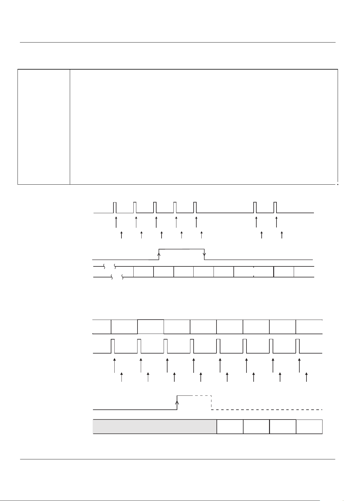
5.2.3 CONTROL 2 Register (Hex address $11)
This register is used to control the functions of the device as described below:
CHKSUM
(Bit 7)
In the Tx mode, when this bit is "1", the checksum generator is enabled. All complete bytes that are
transmitted after this time are used in the checksum calculation.
When this bit goes from "1" to "0", the checksum generator will complete its calculations on the
current byte and the result will be sent as the next two bytes of transmitted data.
In the Rx mode, the "0" to "1" transition of the CHKSUM bit is used at the start of the next byte
received at DEMODIN to manually reset the Rx checksum calculation, see Figure 4. The calculation
can also be reset automatically by a SYNC, SYNT, or RX SYNC WORD detection - see section 5.2.5.
In this case, the Rx checksum calculation starts with the first data byte after the 2-byte sync word has
been detected. The CHKSUM bit can be reset to "0" at any time. The result of the checksum is made
available in the STATUS Register after the reception of every complete byte (See section 5.3.1).
Note that the device is designed to work with any message length, and as a consequence it is not
aware of the position of the checksum within the incoming data message. It thus performs a
checksum assessment after every received byte. The controlling software should use its knowledge
of the system message length in order to determine which RXSUMF reading is valid, i.e. after the
second of the two checksum bytes has been received.
The timing of data bytes relative to the checksum bit is shown in Figure 3 and Figure 4.
READ STATUS
REGISTER
Tx OUTPUT
CHECKSUM based on bytes 3, 4, 5.
TXDAT AF(bit 3)
STATUS REGISTER
1
2
34
5
2 - BYTE
CHECKSUM
67
CHKSUM (bit 7)
CONTROL 2 REGISTER
WRITE TO
Tx DATABUFFER
12
5
6
7
3
4
Figure 3: Checksum Generation in Tx Mode
READ STATUS
REGISTER
RXDATAF (bit 4)
STATUS REGISTER
DEMODIN
(Rx Data)
1
READ Rx
DATA BUFFER
0
23
4
56
7
CHKSUM (bit 7)
CONTROL 2 REGISTER
1
2
3
4
4
CHECK CHECK CHECK CHECK
5
4
+
5
7
6
++
4
5
6
+++
4
5
7
6
RXSUMF (bit 6)
STATUS REGISTER
Figure 4: Checksum Calculation in Rx Mode
 Loading...