

DATA BULLETIN
VSR CODEC WITH
MX812
Features and Applications
• Half-Duplex Voice Storage and Retrieval
• Serial Bus
• On-Chip DRAM Controller
• Up To 2 Minutes of High-Quality
Recorded Audio
• Answering Functions and VoiceNotepad
• Low-Power 5-Volt CMOS
µµ
µProcessor Control
µµ
DRAM CONTROL
PRELIMINARY INFORMATION
• Selectable Sample Rates and “Memory
Size”
MX812DW MX812J
28-pin SOIC 28-pin CDIP
CLOCK
AUDIO OUT
V
BIAS
AUDIO IN
E
BIAS
V
DD
V
SS
CHIP SELECT
SERIAL CLOCK
COMMAND DAT A
REPLY DATA
IRQ
CLOCK
GENERA TOR
DEMOD
CV S D
CODEC
MOD
POWER METER
STATUS REGISTER
SERIAL
C-BUS
INTERFACE
and
LOGIC
STORE/PLA Y/WAIT COMMAND BUFFER
MODE REGISTER
DRAM
CONTROL
WE
CAS
RAS1
A10/R2
A9
A8
A7
A6
A5
A4
A3
A2
A1
A0
D
DGND
EXTERNAL
DRAM
1 or 2 x
1Mbit
DRAM
Chips
or
1 x
4Mbit
DRAM
Chip
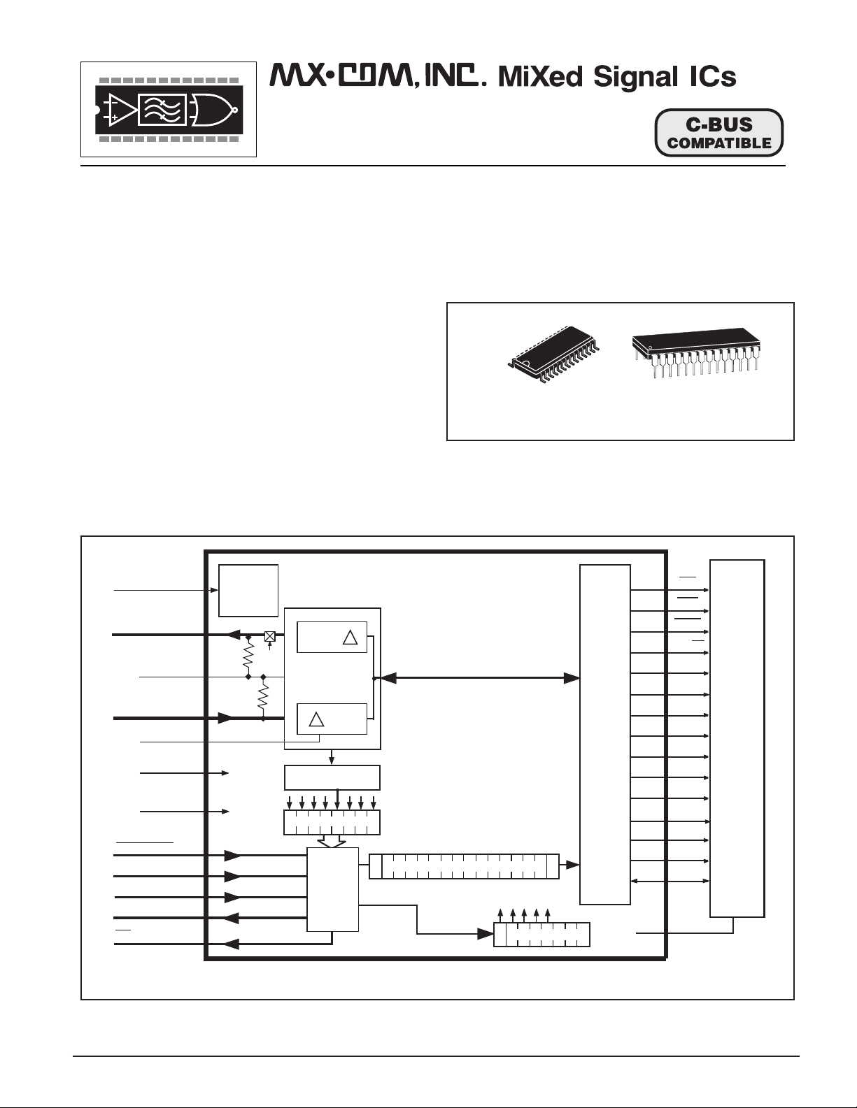
Figure 1 - MX812 Voice Store and Retrieve Codec
© 1997 MX•COM Inc. www.mxcom.com Tele: 800 638-5577 910 744-5050 Fax: 910 744-5054 Doc. # 20480076.003
4800 Bethania Station Road, Winston-Salem, NC 27105-1201 USA All trademarks and service marks are held by their respective companies.
VSR CODEC with DRAM CONTROL 2 MX812 PRELIMINARY INFORMATION
DESCRIPTION
The MX812 is a half-duplex VSR Codec, which
when connected to an audio processing microcircuit
(such as the MX816, 826 or 836), provides the storage
and recovery of speechband audio in attached Dynamic
RAM. The addition of this device will enhance the
communications system by providing cellular radios
with Answering Functions, “Message-Notepad” and
general announcement cababilities.
The MX812 will enable:
• Storage of a speech message for transmission
(replay) at a later time.
• Storage of a received speech message when the
operator is not attending.
• The storage and subsequent replay of speech.
All VSR operating functions are controlled by a
simple serial µProcessor interface which may operate
from the radio’s own µProcessor/Controller.
Input audio from the “Store” output of the audio
processor is digitized by delta modulation and stored
via the DRAM controller, in attached memory.
Audio for replay is recovered from the assigned
memory locations and after demodulation made
available for supply to the “Play” input of the audio
processor. For use with other audio systems, the input/
output audio can be connected to relevant points in
circuit.
The MX812 has no on-chip input or output audio
filtering; this capability must therefore be provided by
the host system. Sampling rates and memory capacity
are selectable to 32kb/s or 63kb/s and 1 x 4Mbit or 2 x
1Mbit respectively, which when used in conjunction
allow control of audio-quality and storage-time.
This low-power CMOS device is available 28-pin
plastic SOIC and 28-pin Cerdip packages.
Pin Function
1 CAS: This output should be connected to the “Column Address Strobe” input pin(s) of all DRAM
devices installed.
2 WE: This output should be connected to the “Write Enable” input pin(s) of all DRAM devices installed.
3D: Digital (speech) data into and out of the VSR Codec. This pin should be connected to the “Data
In” and “Data Out” pins (“D” and “Q”) of DRAM devices.
4 Xtal: The nominal 4.0MHz clock input to the VSR Codec. The signal applied to this device may be
derived from the attached Audio Processor on-chip Xtal Oscillator circuits (see Figures 2 and 3).
Note that the VSR Codec will be able to function and maintain correct DRAM refresh, with Xtal input
frequencies down to 2.0MHz. Compand and Local Decoder time constants will change accordingly
and minimum “C-BUS” timings (Figures 6 and 7) would have to be increased pro-rata.
5 Interrupt Request (IRQ): This Interrupt Request output from the MX812 is ‘wire-OR able’ allowing
the Interrupt Outputs of other peripherals to be commoned and connected to the Interrupt input of the
µProcessor (see the C-BUS Interface and System Applications document). This input has a lowimpedance pulldown to VSS when active, and a high-impedance when inactive.
6 Serial Clock: The C-BUS serial clock input. This clock produced by the µController, is used for
transfer timing of commands and data to and from the VSR Codec. See Timing Diagrams.
7 Command Data: The C-BUS serial (command) data input from the µController. Data is loaded to
this device in 8-bit bytes MSB (B7) first and LSB (B0) last, synchronized to the Serial Clock.
8 Chip Select (CS): The C-BUS data transfer control function. This input is provided by the
µController. Transfer sequences are initiated, completed or aborted by this signal. See Timing
Diagrams.
9 Reply Data: The C-BUS serial data output to the µController. The transmission of reply bytes is
synchronized to the Serial Clock under the control of the Chip Select input. This is a 3-state output
which is held at a high-impedance when not sending data to the µController.
10 V
: The output of the internal analog circuitry bias line, held internally at VDD/2. This pin should be
BIAS
decoupled to VSS by capacitor C2 (see Figure 2).
© 1997 MX•COM Inc. www.mxcom.com Tele: 800 638-5577 910 744-5050 Fax: 910 744-5054 Doc. # 20480076.003
4800 Bethania Station Road, Winston-Salem, NC 27105-1201 USA All trademarks and service marks are held by their respective companies.
VSR CODEC with DRAM CONTROL 3 MX812 PRELIMINARY INFORMATION
Pin Function
11 Audio Out: The analog output to the Audio Processor “Play” input when the VSR Codec is
configured as a Decoder. When configured as an active Decoder but with no Play Page commands
(62H) active, the VSR Codec will play-out an idle pattern of “101010........10s”. When not configured as
a Decoder, or Powersaved (Mode Register), this output will be held at V
resistor. The output at this pin is unfiltered; an external speechband filter – such as that included on
the MX816/826/836 Audio Processors – will be required. Since this output is centered around VDD/2 a
coupling capacitor is required.
via an internal 500kΩ
BIAS
12 E
: The Encoder d.c. internal balancing circuitry line. This pin should be decoupled to VSS by
BIAS
capacitor C4 (see Figure 2). Note that in the ‘Encode’ mode (Mode Register DE and PS both “0”) the
Codec drives this pin to approximately VDD/2 through a very high impedance; it can take more than
one second for the E
voltage to stabilize when power is first applied to this device. A faster start-up
BIAS
can be achieved by setting Bit DE or PS to “1” for 250mS (approx) during power-up. This will cause
the E
pin to be connected to V
BIAS
through a resistance of approximately 100kΩ.
BIAS
13 Audio In: The analog input to the VSR Codec in the Encode mode. When not configured as an
Encoder, or Powersaved (Mode Register), this input will be held at V
via an internal 500kΩ resistor.
BIAS
This pin should be coupled via a capacitor, see Figure 2. As this input does not contain an internal
audio filter, the audio to this pin should be limited to a 3400Hz “speechband” by an external audio filter
– such as included in the MX816/826/836 Audio Processors.
14 VSS: The “analog” ground connection. See D
description.
GND
15 A0:
16 A1:
17 A2:
18 A3:
19 A4:
20 A5:
DRAM address line outputs from the MX812.
These pins should be connected to the corresponding address
inputs of the associated DRAM.
21 A6:
22 A7:
23 A8:
24 A9:
25 A10/R2: A dual function output pin selected by the memory size (MS) bit (Mode Register),
as detailed in the table below:
MS bit DRAMs Connected To This Output
“0” 1Mbits' DRAM No 2 RAS RAS2
“1” 4Mbit DRAM A10 A10 Signal
26 RAS: An output from the VSR Codec which should be connected to the “Row Address Strobe” pin of
the 4Mbit DRAM or the first 1Mbit DRAM, see Figure 4, Example DRAM connections.
27 D
: The digital signal ground connection to the VSR Codec. Both D
GND
and VSS pins should be
GND
connected to the negative side of the d.c. power supply. However, a printed circuit board should be
laid out so that D
is connected as closely as possible to the DRAM section ground pins.
GND
28 VDD: Positive supply rail. A single, stable +5-volt supply is required. Levels and voltages within the
VSR Codec are dependent upon this supply. This pin should be decoupled to VSS via capacitor C5,
located close to the MX812 pins.
© 1997 MX•COM Inc. www.mxcom.com Tele: 800 638-5577 910 744-5050 Fax: 910 744-5054 Doc. # 20480076.003
4800 Bethania Station Road, Winston-Salem, NC 27105-1201 USA All trademarks and service marks are held by their respective companies.
VSR CODEC with DRAM CONTROL 4 MX812 PRELIMINARY INFORMATION
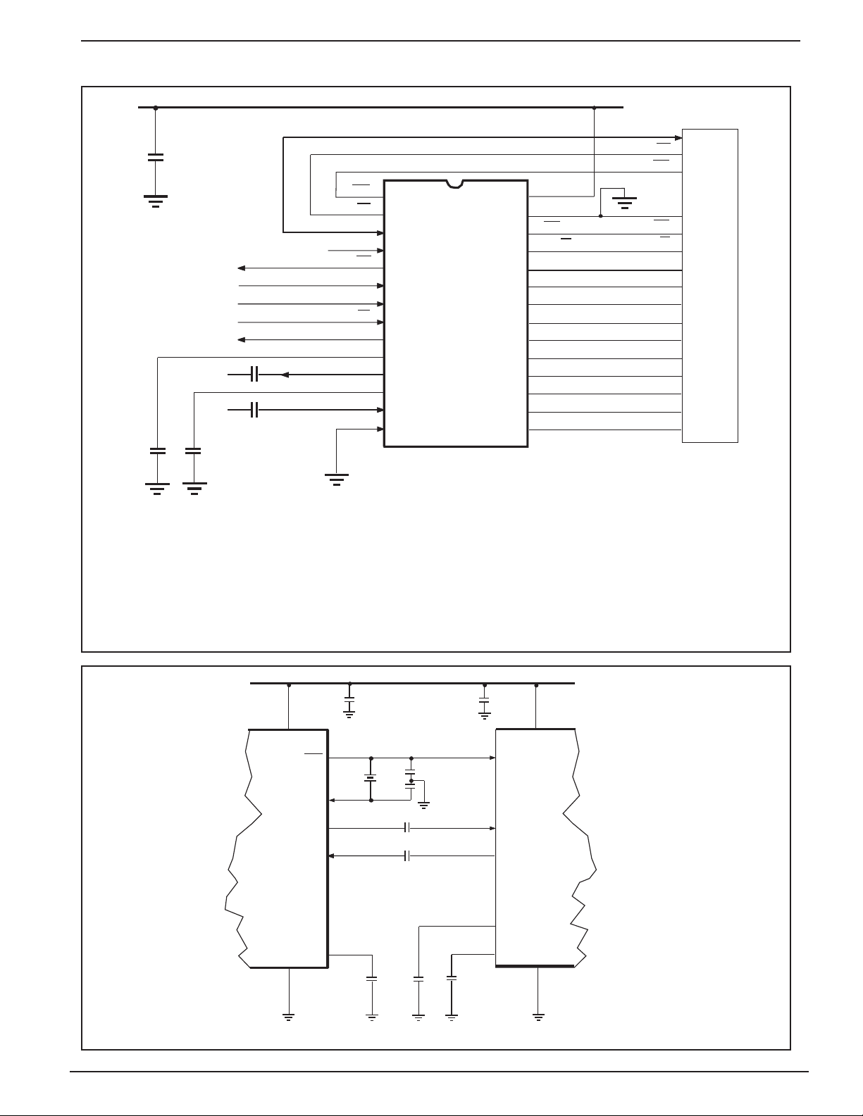
Application Information
V
DD
C
5
V
CAS
1
WE
2
D
SS
IRQ
CS
3
4
5
6
7
8
9
10
11
12
13
14
MX812J
XT AL
SERIAL CLOCK
COMMAND DATA
REPLY DATA
V
C
1
C
3
C
2
C
4
BIAS
AUDIO OUT
E
BIAS
AUDIO IN
V
28
27
26
25
24
23
22
21
20
19
18
17
16
15
DD
D
GND
RAS
A10/R2
A9
A8
A7
A6
A5
A4
A3
A2
A1
A0
WE
CAS
D
RAS
A10/R2
GND
A9
A8
A7
A6
A5
A4
A3
A2
A1
A0
D
D
R
A
M
Component Value
C
1
C
2
C
3
C
4
Tolerance: Capacitors = -50/+100%
Figure 2 - Recommended External Components
+ 5.0V
V
DD
XTAL
XTAL/CLOCK
STORE
Cellular
Audio
PLAY
Processor
eg. MX8n6
Dependent upon the input
impedance of the driven stage
1.0µF
0.1µF
1.0µF non-electrolytic
V
CC
XTAL
AUDIO IN
AUDIO OUT
MX812
E
BIAS
V
BIAS
V
SS
V
BIAS
V
SS
Figure 3 - Interfacing to an Audio Processor
© 1997 MX•COM Inc. www.mxcom.com Tele: 800 638-5577 910 744-5050 Fax: 910 744-5054 Doc. # 20480076.003
4800 Bethania Station Road, Winston-Salem, NC 27105-1201 USA All trademarks and service marks are held by their respective companies.
 Loading...