

MX COM Inc MX809J, MX809LH Datasheet
DATA BULLETIN
MX809
1200bps MSK Modem
1998 MX-COM, Inc. www.mxcom.com Tel: 800 638 5577 336 744 5050 Fax: 336 744 5054 Doc. # 20480036.004
4800 Bethania Station Road, Winston-Salem, NC 27105-1201 USA All trademarks and service marks are held by their respective companies.
PRELIMINARY INFORMATION
Features
Half-Duplex 1200bps MSK Modem
operating under C-BUS control
Software Selectable Checksum
Generation and Error Checking in
accordance with MPT1327
Low Power Operation
Member of DBS800 Family (C-BUS
Compatible)
ä
ä
ä
ää
ä
ä
ää
ä
ä
ä
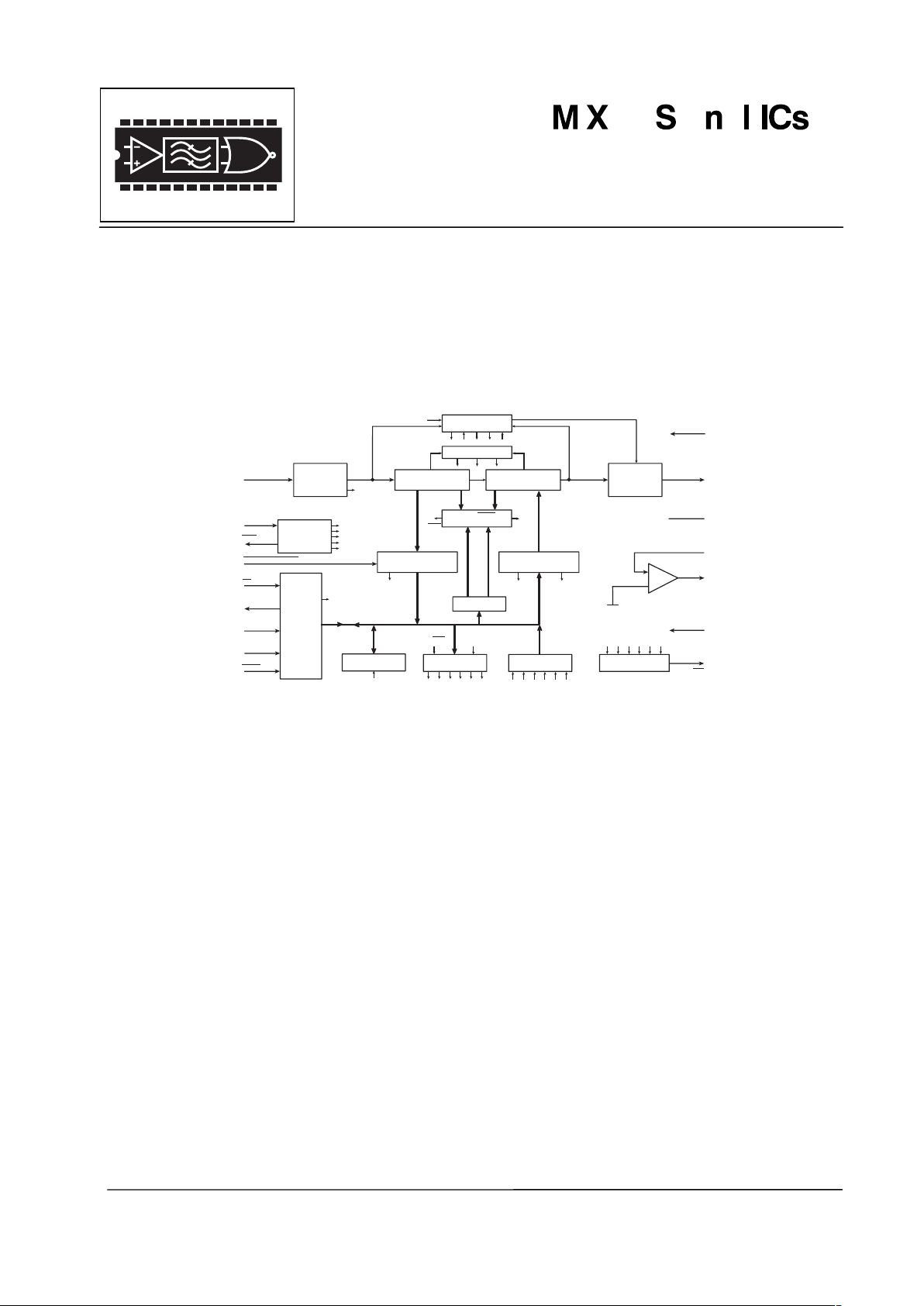
MSK
RECEIVER
CLOCK
GENERATOR
CHECKSUM
GEN/CHECK
BYTE COUNTER
SYNC/
DETECT
SYNC
DATA REGISTER 1 DATA REGISTER 2
MSK
TRANSMITTER
UNCOMMITTED
AMPLIFIER
INTERRUPT
GENERATOR
IRQ
AMP OUT
AMP IN
STATUS
REGISTER
C-BUS
INTERFACE
AND
CONTROL
LOGIC
RX DATA BUFFER TX DATA BUFFER
8-BIT PARALLEL BUS
TX OUT
V
V
V
V
DD
SS
BIAS
BIAS
RECOVERED
CLOCK
RX IN
XTAL/
CLOCK
XTAL
CS
RX FREEFORMAT
REPLY
DATA
SERIAL
CLOCK
COMMAND
DATA
WAKE
CONTROL
REGISTER
ADDRESS
DECODER
ADDRESS
SELECT
SYNC PROGRAM
LOW - HIGH
+
_
INTERRUPT
ENABLE
RX DATA
READY
RX
DETECT
SYNC
RX
DETECT
SYNC
RX SYNC
DETECT
RX SYNC
DETECT
TX DAT A
READY
TX IDLE
RECOVERED
CLOCK
The MX809 is an intelligent, half-duplex 1200-baud MSK Modem, which operates under C-BUS control. This
modem provides software selectable checksum generation and error checking in accordance with MPT1327.
In TX Mode the MX809 will:
1. a) Accept from the host and transmit 8-bit bytes of data as instructed (preamble, sync, address, and data), or
b) Internally calculate and inset a 2 byte checksum based on the preceding 6 bytes f data, or
c) Disable the internal checksum generator and continuously transmit the data supplied.
2. Transmit 1 hang-bit and go to TX idle when all loaded data bytes have been transmitted.
In RX Mode the MX809 will:
1. Detect and carry out bit synchronization within 16 bits.
2. a) Search and detect the user-programmed Sync (or its opposite logic sense) Word and carry out frame
synchronization. Data will then be output in 8-bit bytes via the RX Data Buffer.
b) Use the received checksum to calculate the presence of any errors, setting the Status Register accordingly.
3. Make the incoming data directly available via the RX Data Buffer (RX Freeformat), overriding the synchronization
requirements.
RX input timing is achieved by recovering an RX clock from the incoming data stream. Output tones are
timed to the internally generated TX clock. Filter, register clocks, and transmit MSK tone frequencies are
derived internally from the external Xtal or clock pulse input.
A 4.032MHz Xtal or clock input is required for compliance with the MPT1327 Signaling Specification. Note:
All information contained in this data bulletin is specified using a 4.032MHz Xtal, 1200bps baud rate, with
Mark and Space frequencies of 1200Hz and 1800Hz. The MX809 has a non-committed amplifier on-chip for
general applications in the DBS 800 series.
The MX809 may be used with a 5.0V power supply and is available in the following packages:
24-pin PLCC (MX809LH), and 24-pin CERDIP (MX809J).

MSK Modem 2 MX809
1998 MX-COM, Inc. www.mxcom.com Tel: 800 638 5577 336 744 5050 Fax: 336 744 5054 Doc. # 20480036.004
4800 Bethania Station Road, Winston-Salem, NC 27105-1201 USA All trademarks and service marks are held by their respective companies.
Contents
Section Page
1 Block Diagram................................................................................................................3
2 Signal List.......................................................................................................................4
3 External Components....................................................................................................6
4 General Description.......................................................................................................7
5 Controlling Protocol......................................................................................................7
5.1 Address/Commands............................................................................................................ 7
5.2 Address Select .................................................................................................................... 8
5.3 Write to Control Register ..................................................................................................... 9
5.4 RX Data buffer -- “Read RX Data Buffer” ............................................................................ 9
5.5 TX Data Buffer -- “Write to TX Data Buffer”....................................................................... 10
5.6 SYNC Program -- “Write to SYNC Program”..................................................................... 10
5.7 Read Status Register ........................................................................................................ 10
5.8 Interrupt Request............................................................................................................... 11
5.9 General Reset ................................................................................................................... 11
6 Application ................................................................................................................... 12
6.1 Checksum Generation and Checking................................................................................ 12
6.1.1 Generation..............................................................................................................................12
6.1.2 Checking.................................................................................................................................12
6.2 Modem Performance......................................................................................................... 12
6.3 Modem Timing Information................................................................................................ 13
6.4 TX Timing .......................................................................................................................... 14
6.4.1 TX More Than One Message, SYNC Before Every Message, TX Checksum Enabled .........14
6.4.2 TX More Than One Message, TX Checksum Not Enabled. ...................................................14
6.4.3 TX One Message, TX Checksum Enabled .............................................................................15
6.4.4 TX One Message, TX Checksum Not Enabled.......................................................................15
6.5 RX Timing.......................................................................................................................... 16
6.5.1 RX
SYNCSYNC
/ Required Before Every Message, Rx Checksum Not Enabled ................. 16
6.5.2 RX Additional Data Follows Initial Address (6 Data & 2 Checksum Bytes) Data, RX checksum
Enabled...................................................................................................................................16
7 Performance Specifications........................................................................................17
7.1 Electrical Specifications..................................................................................................... 17
7.1.1 Absolute Maximum Limits.......................................................................................................17
7.1.2 Operating Limits......................................................................................................................17
7.1.3 Operating Characteristics .......................................................................................................18
7.1.4 Timing.....................................................................................................................................20
7.2 Packages........................................................................................................................... 21
MXCOM, Inc. reserves the right to change specifications at any time without notice.

MSK Modem 3 MX809
1998 MX-COM, Inc. www.mxcom.com Tel: 800 638 5577 336 744 5050 Fax: 336 744 5054 Doc. # 20480036.004
4800 Bethania Station Road, Winston-Salem, NC 27105-1201 USA All trademarks and service marks are held by their respective companies.
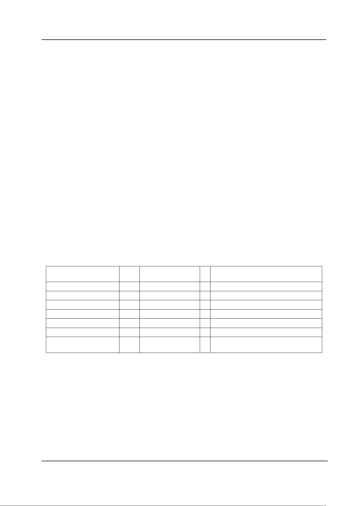
1 Block Diagram
ä
ä
ä
ää
ä
ä
ää
ä
ä
ä
MSK
RECEIVER
CLOCK
GENERA T OR
CHECKSUM
GEN/CHECK
BYTE COUNTER
SYNC/
DETECT
SYNC
DATA REGISTER 1 DATA REGISTER 2
MSK
TRANSMITTER
UNCOMMITTED
AMPLIFIER
INTERRUPT
GENERA T OR
IRQ
AMP OUT
AMP IN
ST ATUS
REGISTER
C-BUS
INTERFACE
AND
CONTROL
LOGIC
RX DATA BUFFER TX DATA BUFFER
8-BIT PARALLEL BUS
TX OUT
V
V
V
V
DD
SS
BIAS
BIAS
RECOVERED
CLOCK
RX IN
XT AL/
CLOCK
XT AL
CS
RX FREEFORMA T
REPLY
DAT A
SERIAL
CLOCK
COMMAND
DAT A
WAKE
CONTROL
REGISTER
ADDRESS
DECODER
ADDRESS
SELECT
SYNC PROGRAM
LOW - HIGH
+
_
INTERRUPT
ENABLE
RX DATA
READY
RX
DETECT
SYNC
RX
DETECT
SYNC
RX SYNC
DETECT
RX SYNC
DETECT
TX DATA
READY
TX IDLE
RECOVERED
CLOCK
Figure 1: Block Diagram
MSK Modem 4 MX809
1998 MX-COM, Inc. www.mxcom.com Tel: 800 638 5577 336 744 5050 Fax: 336 744 5054 Doc. # 20480036.004
4800 Bethania Station Road, Winston-Salem, NC 27105-1201 USA All trademarks and service marks are held by their respective companies.
2 Signal List
Pin Signal Description
1
Xtal
This is the output of the on-chip clock oscillator. External components are
required at this output when a Xtal is used. See Figure 2. Inset
2 Xtal/Clock
This is the input to the on-chip clock oscillator inverter. A Xtal or externally
derived clock should be connected here. See Figure 2. Inset
3
IRQ
The output of this pin indicates an interrupt condition to the microcontroller by
going to a logic “0”. This is a “wire-or-able” output that enables the connection of
up to 8 peripherals to 1 interrupt port on the microcontroller. This pin is an opendrain output, and therefore has a low impedance pulldown to logic “0” when active
and a high impedance when inactive. The conditions that cause interrupts are
indicted in the Status Register and are shown in Table 2. The system
IRQ
line
requires a pull-up resistor to V
DD
.
4 N/C
5 N/C
6
Freeformat RX
When this input is logic “0” in the RX Mode, it allows received data to be read
from the RX Data Buffer via the Reply Data line without having to achieve byte
synchronization (SYNC/
SYNC) first. Data will continue to be available after this
input goes to a logic “1” until either a SYNC or
SYNCPrime Bit is set or the
modem is set to TX Mode. When held at a logic “1” the modem operates
normally. This pin has an internal 1M pull-up resistor.
Note
: If this input is held at a logic “0” in the TX Mode, the RX Data Ready bit in
the Status Register may occasionally be set, but not cause an interrupt. If this
input is a logic “0” when going into the RX Mode, and RX Data Ready interrupt
may be generated immediately (in this case the first byte of RX data should be
ignored).
7V
BIAS
The internal circuitry bias line, this is held at VDD/2. This pin must be decoupled
to V
SS
by capacitor C3. See Figure 2.
8 Amp In The inverting input to the on-chip uncommitted amplifier.
9 Amp Out The output of the on-chip uncommitted amplifier.
10 RX In This is the 1200 baud, 1200Hz/1800Hz received MSK signal input. The input
signal to this pin must be AC coupled via capacitor C4. See Figure 2.
11 N/C
12 V
SS
Negative Supply (GND)
13 TX Out This is the 1200 baud, 1200Hz/1800Hz MSK TX output. When not transmitting
data the output impedance of this pin is high. On power-up this output can be any
level. A General Reset command is required to ensure that this output attains
V
BIAS
initially.
14 N/C
15 N/C
16 N/C
17 Reply Data This is the C-BUS serial data output to the microcontroller. The transmission of
Reply Data bytes is synchronized to the Serial Clock under the
CS
input. This 3state output is held high impedance when not sending data to the microcontroller.
See Section 6 and Section 7.1.4.
18 N/C
19
CS
Select Chip . This is the ‘C-BUS’ data loading control function. This input is
provided by the microcontroller. Data transfer sequences are initiated, completed
or aborted by the
CS signal. See Section 6 and Section 7.1.4.
20 Command Data This is the ‘C-BUS’ serial data input from the microcontroller. Data is loaded to
this device in 8-bit bytes, MSB (bit 7) first and LSB (bit 0) last, synchronized to the
Serial Clock. See Section 6 and Section 7.1.4.
MSK Modem 5 MX809
1998 MX-COM, Inc. www.mxcom.com Tel: 800 638 5577 336 744 5050 Fax: 336 744 5054 Doc. # 20480036.004
4800 Bethania Station Road, Winston-Salem, NC 27105-1201 USA All trademarks and service marks are held by their respective companies.
Pin Signal Description
21 Serial Clock
This is the ‘C-BUS’ serial Clock input. This clock, produced by the
microcontroller, is used for transfer timing of commands and data to and from the
MSK Modem. See Section 6 and Section 7.1.4.
22 Address Select This pin enables two MX809s to be used on the same C-BUS, providing full-
duplex operation. When at a logic “1” Address/Command bytes (with the
exception of a General Reset) must have bit 3 set to a logic “1” to address this
device. See Table 5 and Table 6.
23
Wake
This input can be used to reactivate the MX809 from Powersave. The device will
be in Powersave when both this pin and bit 2 of the Control Register are set to
logic “1”. Recovery from Powersave is achieved by putting either the
Wake pin or
the Powersave bit in the Control Register to logic “0”. This allows MX809
activation by the microcontroller or an external signal, such as R.S.S.I. or Carrier
Detect. See Table 3.
24 V
DD
Positive supply. A single +5.0V power supply is required. Levels and voltages
within the MSK Modem are dependent upon this supply.
Table 1: Signal List
TX Idle RX Data Ready TX Data Ready
RX SYNC Detect RX Sync Detect
Interrupt outputs can be disabled by bit 3 of the Control Register
Table 2:
IRQ
Conditions
Powersave (CR bit 2)
Wake
MX809 Condition
1
0
1
0
1
1
0
0
Powersave
Enabled
Enabled
Enabled
Table 3:
Wake
and Powersave Conditions
MSK Modem 6 MX809
1998 MX-COM, Inc. www.mxcom.com Tel: 800 638 5577 336 744 5050 Fax: 336 744 5054 Doc. # 20480036.004
4800 Bethania Station Road, Winston-Salem, NC 27105-1201 USA All trademarks and service marks are held by their respective companies.
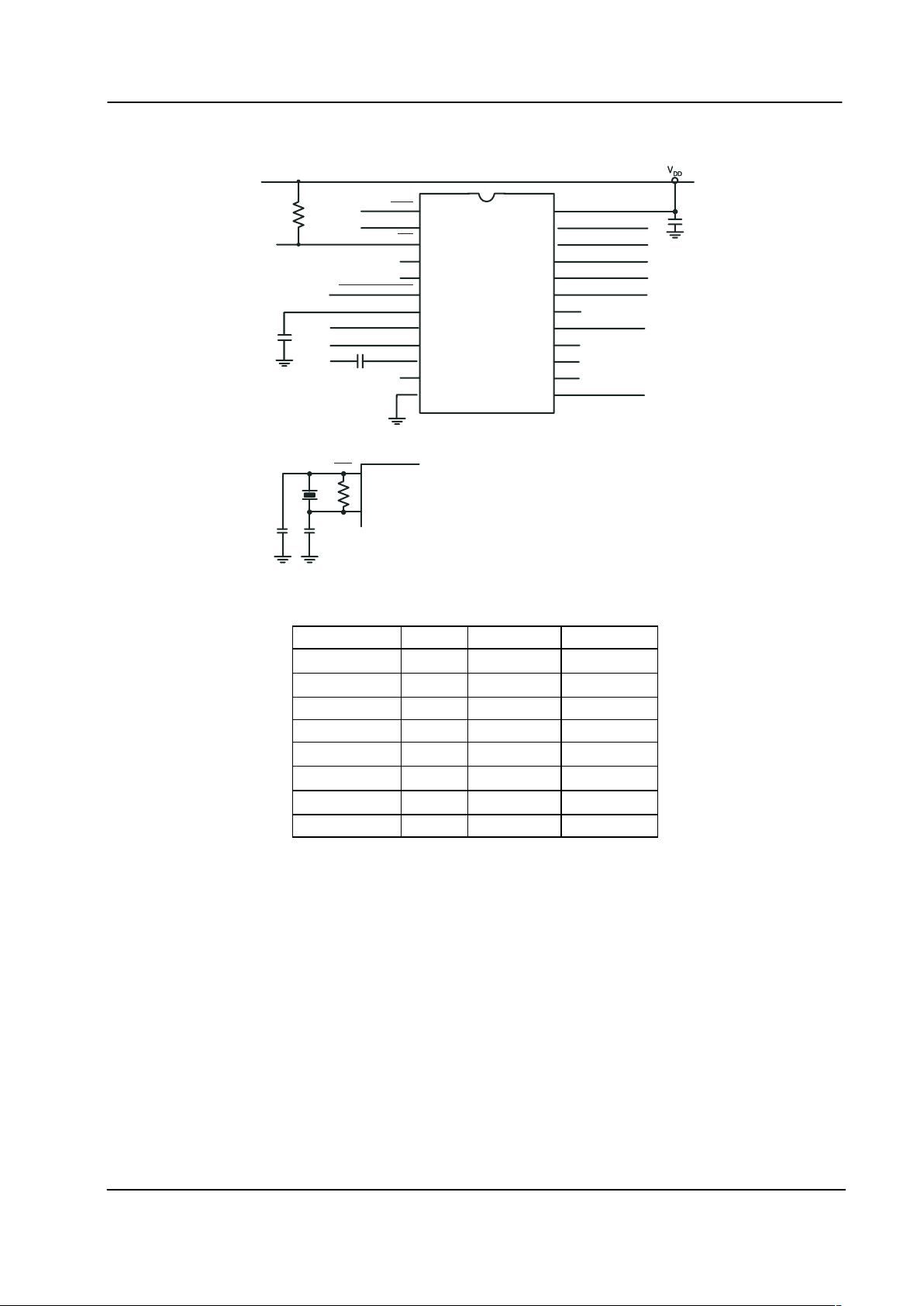
3 External Components
➤
➤
➤
➤
➤
➤
➤
➤
➤
➤
➤
➤
➤
➤
➤
➤
R2
SEE INSET
XTAL
XTAL/CLOCK
IRQ
RX FREEFORMAT
V
BIAS
AMP IN
AMP OUT
C3
1
2
3
4
5
6
7
8
9
10
11
12
13
14
15
16
17
18
19
20
21
22
23
24
MX809J
RX IN
C4
V
SS
V
DD
WAKE
ADDRESS SELECT
SERIAL CLOCK
COMMAND DA TA
CS
REPLY DATA
TX OUT
C5
INSET
XTAL
C2 C1
X1 R1
1
2
XTAL/CLOCK
MX809J
Figure 2: Recommended External Components
Component Notes Value Tolerance
R1
1.0M
±10%
R2
22.0K
±10%
C1 1 33pF ±20%
C2 1 33pF ±20%
C3
1.0F
±20%
C4
0.1F
±20%
C5
1.0F
±20%
X1 1 4.032MHz
Table 4: Recommended External Components
Recommended External Component Notes:
1. Xtal circuit capacitors C1 (CD) and C2 (CG) shown in Inset 2 are recommended in accordance with MXCOM’s Crystal Oscillator Application Note.
MSK Modem 7 MX809
1998 MX-COM, Inc. www.mxcom.com Tel: 800 638 5577 336 744 5050 Fax: 336 744 5054 Doc. # 20480036.004
4800 Bethania Station Road, Winston-Salem, NC 27105-1201 USA All trademarks and service marks are held by their respective companies.
4 General Description
The MX809 is an intelligent, half-duplex 1200-baud MSK Modem, which operates under C-BUS control. This
modem provides software selectable checksum generation and error checking in accordance with MPT1327.
In TX Mode the MX809 will:
1. a) Accept from the host and transmit 8-bit bytes of data as instructed (preamble, sync, address, and data), or
b) Internally calculate and inset a 2 byte checksum based on the preceding 6 bytes of data, or
c) Disable the internal checksum generator and continuously transmit the data supplied.
2. Transmit 1 hang-bit and go to TX idle when all loaded data bytes have been transmitted.
In RX Mode the MX809 will:
1. Detect and carry out bit synchronization within 16 bits.
2. a) Search and detect the user-programmed Sync (or its opposite logic sense) Word and carry out frame
synchronization. Data will then be output in 8-bit bytes via the RX Data Buffer.
b) Use the received checksum to calculate the presence of any errors, setting the Status Register accordingly.
3. Make the incoming data directly available via the RX Data Buffer (RX Freeformat), overriding the synchronization
requirements.
RX input timing is achieved by recovering an RX clock from the incoming data stream. Output tones are
timed to the internally generated TX clock. Filter, register clocks, and transmit MSK tone frequencies are
derived internally from the external Xtal or clock pulse input.
A 4.032MHz Xtal or clock input is required for compliance with the MPT1327 Signaling Specification. Note:
All information contained in this data bulletin is specified using a 4.032MHz Xtal, 1200bps baud rate, with
Mark and Space frequencies of 1200Hz and 1800Hz. The MX809 has a non-committed amplifier on-chip for
general applications in the DBS 800 series.
5 Controlling Protocol
Control of the functions within the MX809 MSK Modem is by a group of Address/Commands and appended
data instructions from the system microcontroller. Two separate MSK Modems can be addressed. The use
of these A/Cs is detailed in the following paragraphs and tables.
Command Assignment Address/Command
Binary
Command Data
HEX
MSB LSB
General Reset 01 00000001 Control Register bits set to logic “0”
Write to Control Register 40 01000000 + 1 byte instruction to Control Register
Read Status Register 41 01000001 + 1 byte reply from Status Register
Read RX Data Buffer 42 01000010 + 1 byte of data from RX Data Buffer
Write to TX Data Buffer 43 01000011 + 1 byte of data to TX Data Buffer
Write to SYNC Program 44 01000100 + 2 bytes of SYNC Word to SYNC
Program. Register
Table 5: Modem No. 1 C-BUS Address/Commands – (Address Select input at a logic “0”)
5.1 Address/Commands
Instructions and data transactions to and from the MX809 consist of an Address/Command (A/C) byte
followed by either further instructions or data, or a Status or RX Data Reply.
Control and configuration is by writing instructions from the microcontroller to the Control Register [40
H
(48H)].
Reporting of the MX809 configuration is by reading the Status Register [41
H
(49H)]. Instructions and data are
transferred via C-BUS in accordance with the timing information given in Figure 11.
Data to be transmitted as MSK is sent to the TX Data Buffer via the Command Data line. Received data is
read from the RX Data buffer via the Reply Data line.
Instructions and data transactions to and from this device are preceded by the relevant A/C.
 Loading...