DATA BULLETIN
MX805A
1998 MX-COM, Inc. www.mxcom.com Tel: 800 638 5577 336 744 5050 Fax: 336 744 5054 Doc. # 20480116.004
4800 Bethania Station Road, Winston-Salem, NC 27105-1201 USA All trademarks and service marks are held by their respective companies.
Sub-Audio Signaling
Processor
Features
Non-predictive CTCSS Tone Decoder
DCS Sub-Audio Signal demodulator
CTCSS /NRZ Encoder with TX level
adjustment and lowpass filter output
stage with optional NRZ pre-emphasis
Selectable Sub-Audio bandstop filter
NoTone (CTCSS RX) period timer
Low Power Operation
Member of DBS800 Family (C-BUS
Compatible)
RX SUB-AUDIO
IN
RX LPF
RX AMP
AMP IN
AMP OUT
RX SUB-AUDIO
OUT
COMPARATOR
AMP
COMPARATOR
NRZ RX
DATA AND
BAUD RATE
EXTRACTOR
+
+
_
_
DIGITAL
NOISE
FILTER
FREQUENCY
ASSESMENT
NOTONE
TIMER
FREQUENCY
MEASUREMENT
C-BUS
INTERFACE
AND
CONTROL
LOGIC
TX LEVEL
ADJUST
NOTONE
COMMAND DA TA
REPLY DATA
INTERRUPT
SERIAL CLOCK
WAKE
ADDRESS SELECT
TX SUB-AUDIO
OUT
TX SUB-AUDIO LPF
AUDIO OUT
AUDIO BYPASS
CLOCK
GENERAT OR
AUDIO IN
XTAL/
CLOCK
XTAL
IN
OUT
V
DD
V
SS
V
BIAS
NRZ
TX DAT A
NRZ RX
BAUD RATE
NRZ
RX DATA
CTCSS SUB-
AUDIO FREQUENCY
CHIP SELECT
RAW NRZ DATA
RX
TX
SUB-AUDIO BANDSTOP
AUDIO SIGNAL PATH
VARIABLE
BANDWIDTH
180Hz/260Hz
DATA BUFFER
AND
SHIFT REGISTER
The MX805A is a sub-audio frequency signaling processor that provides outband audio and digital signaling
capability for LMR systems. Designed for the transmission and non-predictive reception of Continuous Tone
Controlled Squelch (CTCSS) tones and other non-standard frequencies, the MX805A also handles NonReturn-to Zero (NRZ) data reception and transmission to provide Digitally Coded Squelch (DCS/DPL
TM
) and
LTR
TM
signaling.
Setting the MX805A functions and modes is accomplished by data loaded from the microcontroller to the
controlling registers within the device. Reply Data and Interrupt protocol keep the microcontroller up to date
on the operational status of the circuitry. CTCSS tone data for transmission is generated in the
microcontroller, loaded to the CTCSS TX Frequency Register, encoded and output as a tone via the TX Subaudio LPF. Received non-predicted CTCSS tone frequencies are measured and the resulting data, in the
form of a 2-byte data word, is presented to the microcontroller for matching against a lookup table. Noise
filtering is provided to improve the signal quality prior to measurement. NRZ coded data streams for
transmission, when generated within a microcontroller, are loaded to the NRZ TX Data Buffer and output, in
8-bit bytes, through the lowpass filter circuitry as subaudible signals. DCS turnoff tones can be added to the
data signals by switching the MX805A to the CTCSS transmit mode at the appropriate time. NRZ coding is
produced by the microcontroller and translated to subaudio signals by the MX805A. Received NRZ data is
filtered, detected, and placed into the NRZ Data Register, which is then available for transfer (one byte at a
time) to the microcontroller for decoding by software. Clock extraction circuitry is provided on-chip. TX ad RX
baud rates are selectable.
Hardware and software are designed to allow consecutive addressing of two MX805A Sub-Audio Signaling
Processors to achieve multi-mode duplex operation. Powersaving may be controlled by software or by an
input dedicated to the purpose.
The MX805A may be used with a 5.0V power supply and is available in the following packages:
24-pin SOIC (MX805ADW), 24-pin PLCC (MX805ALH), and 24-pin PDIP (MX805AP).

Sub-Audio Signaling Processor 2 MX805A
1998 MX-COM, Inc. www.mxcom.com Tel: 800 638 5577 336 744 5050 Fax: 336 744 5054 Doc. # 20480116.004
4800 Bethania Station Road, Winston-Salem, NC 27105-1201 USA All trademarks and service marks are held by their respective companies.
Contents
Section Page
1 Block Diagram................................................................................................................4
2 Signal List.......................................................................................................................5
3 External Components....................................................................................................7
3.1 Input configurations ............................................................................................................. 8
3.1.1 Using and External Op-Amp.....................................................................................................8
4 General Description.......................................................................................................9
4.1 Glossary .............................................................................................................................. 9
4.2 Operating Modes................................................................................................................. 9
4.2.1 NRZ Encoding...........................................................................................................................9
4.2.2 CTCSS Encoding......................................................................................................................9
4.2.3 NRZ Decoding ........................................................................................................................10
4.2.4 CTCSS Decoding....................................................................................................................10
5 Controlling Protocol....................................................................................................10
5.1 MX805A Internal Registers................................................................................................ 10
5.1.1 Control Register (70H/78H) ....................................................................................................10
5.1.2 Status Register (71H/79H)......................................................................................................10
5.1.3 CTCSS Rx Frequency Register (72H/7AH)............................................................................10
5.1.4 CTCSS Tx Frequency/NRZ Tx or Rx Baud Rate Register (73H/7BH) ...................................10
5.1.5 NRZ Rx Data Register (74H/7CH)..........................................................................................10
5.1.6 NRZ Tx Data Register (75H/7DH) ..........................................................................................10
5.1.7 Gain Set Register (76H/7EH)..................................................................................................10
5.2 Address/Commands.......................................................................................................... 11
5.2.1 Write to Control Register - A/C 70H (78H) followed by 1 byte of Command Data..................12
5.2.2 General Reset.........................................................................................................................12
5.2.3 Read Status Register –A/C 71H (79H) followed by 1 byte of Rely Data.................................13
5.2.4 Read CTCSS RX Frequency Register –A/C 72H (7AH) followed by 2 bytes of Reply Data ..13
5.2.5 Write to CTCSS TX Frequency/NRZ Baud Data Rate Register –A/C 73H (7BH) followed
by 2 bytes of Command Data. ................................................................................................15
5.2.6 Read NRZ RX Data Register – A/C 74H (7CH) followed by 1 byte Reply Data.....................17
5.2.7 Write to NRZ TX Data Register – A/C 75H (7DH) followed by 1 byte of Command Data. .....17
5.2.8 Write to Gain Set Register – A/C 76H (7EH) followed by 1 byte of Command Data..............17

Sub-Audio Signaling Processor 3 MX805A
1998 MX-COM, Inc. www.mxcom.com Tel: 800 638 5577 336 744 5050 Fax: 336 744 5054 Doc. # 20480116.004
4800 Bethania Station Road, Winston-Salem, NC 27105-1201 USA All trademarks and service marks are held by their respective companies.
6 Performance Specifications........................................................................................18
6.1 Electrical Specifications..................................................................................................... 18
6.1.1 Absolute Maximum Limits..............................................................................................................18
6.1.2 Operating Limits ............................................................................................................................18
6.1.3 Operating Characteristics..............................................................................................................19
6.1.4 Timing............................................................................................................................................22
6.2 Packages........................................................................................................................... 23
MXCOM, Inc. reserves the right to change specifications at any time without notice.

Sub-Audio Signaling Processor 4 MX805A
1998 MX-COM, Inc. www.mxcom.com Tel: 800 638 5577 336 744 5050 Fax: 336 744 5054 Doc. # 20480116.004
4800 Bethania Station Road, Winston-Salem, NC 27105-1201 USA All trademarks and service marks are held by their respective companies.
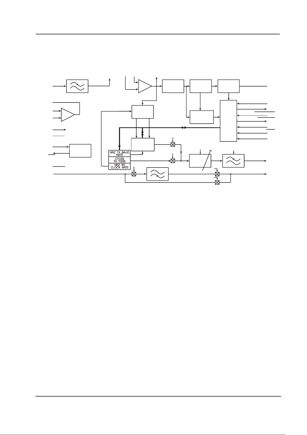
1 Block Diagram
RX SUB-AUDIO
IN
RX LPF
RX AMP
AMP IN
AMP OUT
RX SUB-AUDIO
OUT
COMPARATOR
AMP
COMPARATOR
NRZ RX
DATA AND
BAUD RATE
EXTRACTOR
+
+
_
_
DIGITAL
NOISE
FILTER
FREQUENCY
ASSESMENT
NOTONE
TIMER
FREQUENCY
MEASUREMENT
C-BUS
INTERFACE
AND
CONTROL
LOGIC
TX LEVEL
ADJUST
NOTONE
COMMAND DATA
REPL Y DAT A
INTERRUPT
SERIAL CLOCK
WAKE
ADDRESS SELECT
TX SUB-AUDIO
OUT
TX SUB-AUDIO LPF
AUDIO OUT
AUDIO BYPASS
CLOCK
GENERAT OR
AUDIO IN
XTAL/
CLOCK
XTAL
IN
OUT
V
DD
V
SS
V
BIAS
NRZ
TX DATA
NRZ RX
BAUD RATE
NRZ
RX DATA
CTCSS SUB-
AUDIO FREQUENCY
CHIP SELECT
RAW NRZ DATA
RX
TX
SUB-AUDIO BANDSTOP
AUDIO SIGNAL PATH
VARIABLE
BANDWIDTH
180Hz/260Hz
DATA BUFFER
AND
SHIFT REGISTER
Figure 1: Block Diagram

Sub-Audio Signaling Processor 5 MX805A
1998 MX-COM, Inc. www.mxcom.com Tel: 800 638 5577 336 744 5050 Fax: 336 744 5054 Doc. # 20480116.004
4800 Bethania Station Road, Winston-Salem, NC 27105-1201 USA All trademarks and service marks are held by their respective companies.
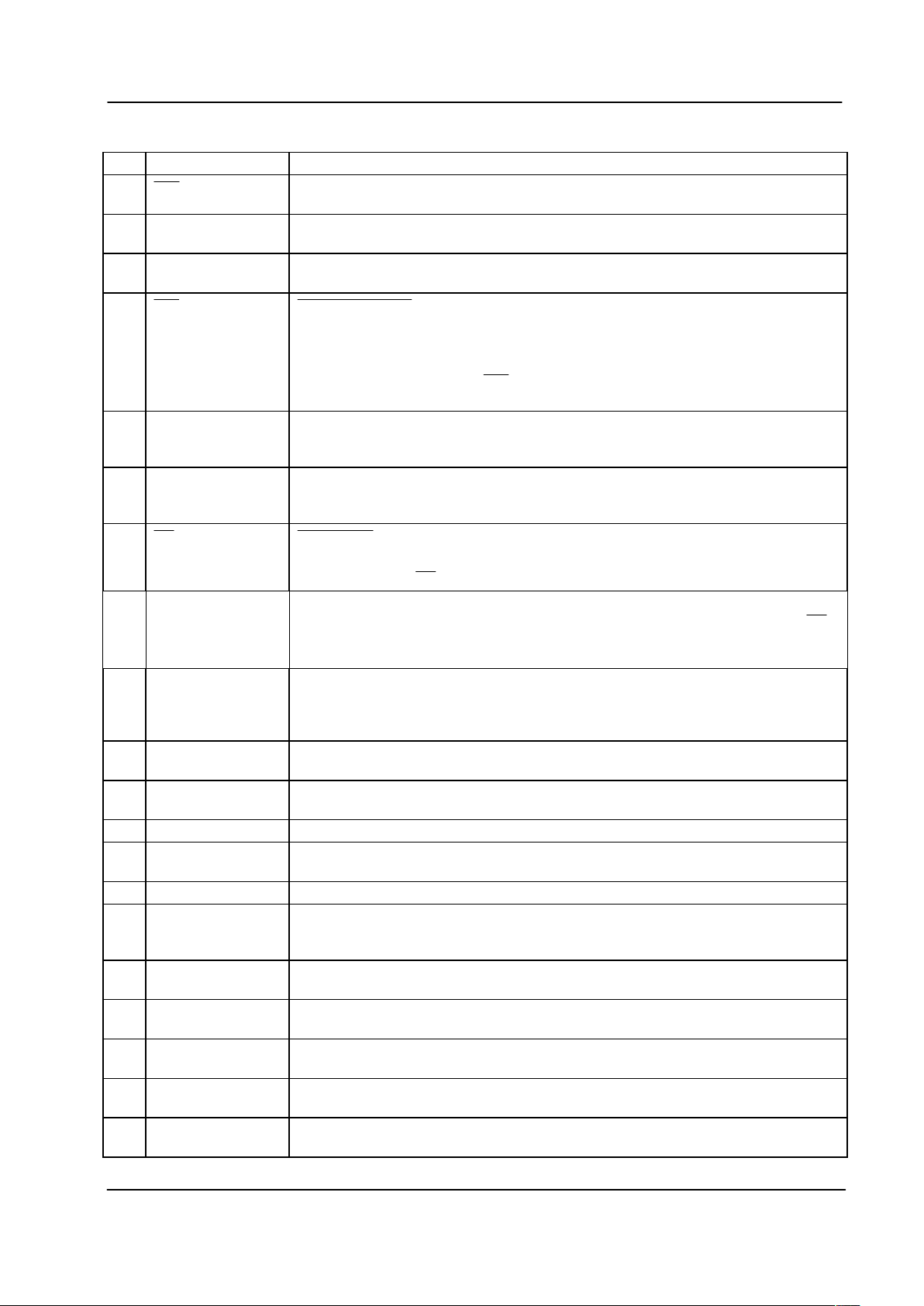
2 Signal List
Pin Signal Description
1
Xtal
The output from the on-chip clock oscillator inverter. External components are
required at this input when a Xtal input is used. See Figure 2.
2 Xtal/Clock
The input to the clock oscillator inverter. A Xtal or externally derived clock should
be connected here.
3 Address Select This input enables two MX805A’s to be used on the same C-BUS to provide dull-
duplex operation. See Table 4 and Table 5.
4
IRQ Request Interrupt . The output of this pin indicates an interrupt condition to the
microcontroller by going to a logic ‘0”. This ‘wire-or-able’ output allows the
connection of up to 8 peripherals to 1 interrupt port on the microcontroller. This
pin has a low impedance pulldown to logic ‘0’ when active, and a high impedance
when inactive. The system
IRQ line requires 1 pull-up resistor to VDD. The
conditions that cause interrupts are indicated in the Table 5 and Table 7.
5 Serial Clock
This is the ‘C-BUS’ serial Clock input. This clock, produced by the
microcontroller, is used for transfer timing of commands and data to and from the
MX805A. See timing diagrams.
6 Command Data This is the ‘C-BUS’ serial data input from the microcontroller. Data is loaded to
this device in 8-bit bytes, MSB (bit 7) first and LSB (bit 0) last, synchronized to the
Serial Clock. See Timing diagrams.
7
CS
Select Chip . This is the ‘C-BUS’ data loading control function. This input is
provided by the microcontroller. Data transfer sequences are initiated, completed
or aborted by the
CS signal. See Timing diagrams.
8 Reply Data This is the ‘C-BUS’ serial data output to the microcontroller. The transmission of
Reply Data bytes is synchronized to the Serial Clock under the control of the
CS
input. This 3-state output is held at high impedance when not sending data to the
microcontroller. See Timing Diagrams
9 TX Sub-Audio Out This is the subaudio output (pure or NRZ derived). Signals are band limited. The
TX Output Filter had a variable bandwidth (See Table 9). This output is at V
BIAS
(a) when the NRZ Encoder is enabled but no data is being transmitted, (b) when
the MX805A is placed in the Powersave All condition.
10 Audio In This is the input to the switched sub-audio bandstop (highpass) filter. It is
internally biased, and should be AC coupled by capacitor C7.
11 Audio Out This is the output of the audio signal path (filter or bandpass). It is controlled by
the Control Register. When disabled, the pin is held at V
BIAS
.
12 V
SS
Negative Supply (GND)
13 RX Amp In (-)
This is the inverting input to the on-chip RX Input Amp. (See Figure 2, Figure 3,
and Figure 4).
14 RX Amp In (+) This is the non-inverting input to the on-chip RX Input Amp.
15 RX Amp Out This is the output of the on-chip RX Input Op-Amp. This circuit may be used, with
external components, as a signal amplifier and anti-aliasing filter prior to the RX
Lowpass Filter, or for other purposes. See Figure 2 for Component details.
16 RX Sub-Audio In This is the received Sub-Audio (CTCSS/NRZ) input. It is internally referenced to
V
BIAS
. This signal to this pin should be AC coupled or biased. See Figure 2.
17 RX Sub-Audio Out
This is the output of the RX lowpass filter. It may be coupled into the on-chip
amplifier or comparator as required.
18 V
BIAS
The internal circuitry bias line, held at VDD/2. This pin must be decoupled to V
SS
by capacitor C8. See Figure 2.
19 Comparator In (-) This is the inverting input to the on-chip ‘comparator’ amplifier. See Figure 2,
Figure 3, and Figure 4.
20 Comparator In (+)
This is the non-inverting input to the on-chip ‘comparator’ amplifier. See Figure 2,
Figure 3, and Figure 4.

Sub-Audio Signaling Processor 6 MX805A
1998 MX-COM, Inc. www.mxcom.com Tel: 800 638 5577 336 744 5050 Fax: 336 744 5054 Doc. # 20480116.004
4800 Bethania Station Road, Winston-Salem, NC 27105-1201 USA All trademarks and service marks are held by their respective companies.
Pin Signal Description
21 Comparator Out
This is the output of the ‘comparator’ amplifier. This node is also connected
internally to the input of the /digital Noise Filter (See Figure 1). When both
decoders (CTCSS or NRZ) are powersaved, this output is at a logic ‘0’.
22 Notone Timing External RC components connected to this pin form the timing mechanism of a
Notone period timer. The external network determines the “charge rate” of the
timer to V
BIAS
. The expiration of the timer will cause an interrupt. This function is
only used in the CTCSS RX mode. See page 9.
23
Wake
This ‘real time’ input can be used to reactivate the MX805A from the ‘Powersave
All’ condition using an externally derived signal. The MX805A will be in
‘Powersave All’ condition when both this pin and bit 0 of the Control Register are
set to a logic ‘1’. Recovery from ‘Powersave All’ is achieved by putting either the
Wake
pin or the ‘Powersave All” bit at logic ‘0’. This allows MX805A activation by
the microcontroller or an external signal, such as RSSI or Carrier Detect.
24 V
DD
Positive Supply. A single 5.0V regulated supply is required.
Note: More information on external components and the DBS800 system integration of the MX805A are
contained in the DBS800 System Support Documentation. Guidance on the generation and
manipulation of NRZ and RX and TX data is given in the DBS800 Application support documentation.
C-BUS: This is MX-COM’s proprietary standard for the transmission of commands and data between a
microcontroller and DBS8000 microcircuits. It may be used with any microcontroller, and can, if
desired, take advantage of the hardware and serial I/O functions embodied into many types of
microcontroller. The C-BUS data rate is determined by the microcontroller.
Table 1: Signal List
RX CTCSS Tone Measurement Completed
CTCSS NOTONE Timer Expired
1 NRZ RX Data Byte Received
New NRZ Data Received Before Last Byte Read
NRZ TX Buffer Ready
NRZ Data Transmission Complete
Table 2: Interrupt Conditions

Sub-Audio Signaling Processor 7 MX805A
1998 MX-COM, Inc. www.mxcom.com Tel: 800 638 5577 336 744 5050 Fax: 336 744 5054 Doc. # 20480116.004
4800 Bethania Station Road, Winston-Salem, NC 27105-1201 USA All trademarks and service marks are held by their respective companies.
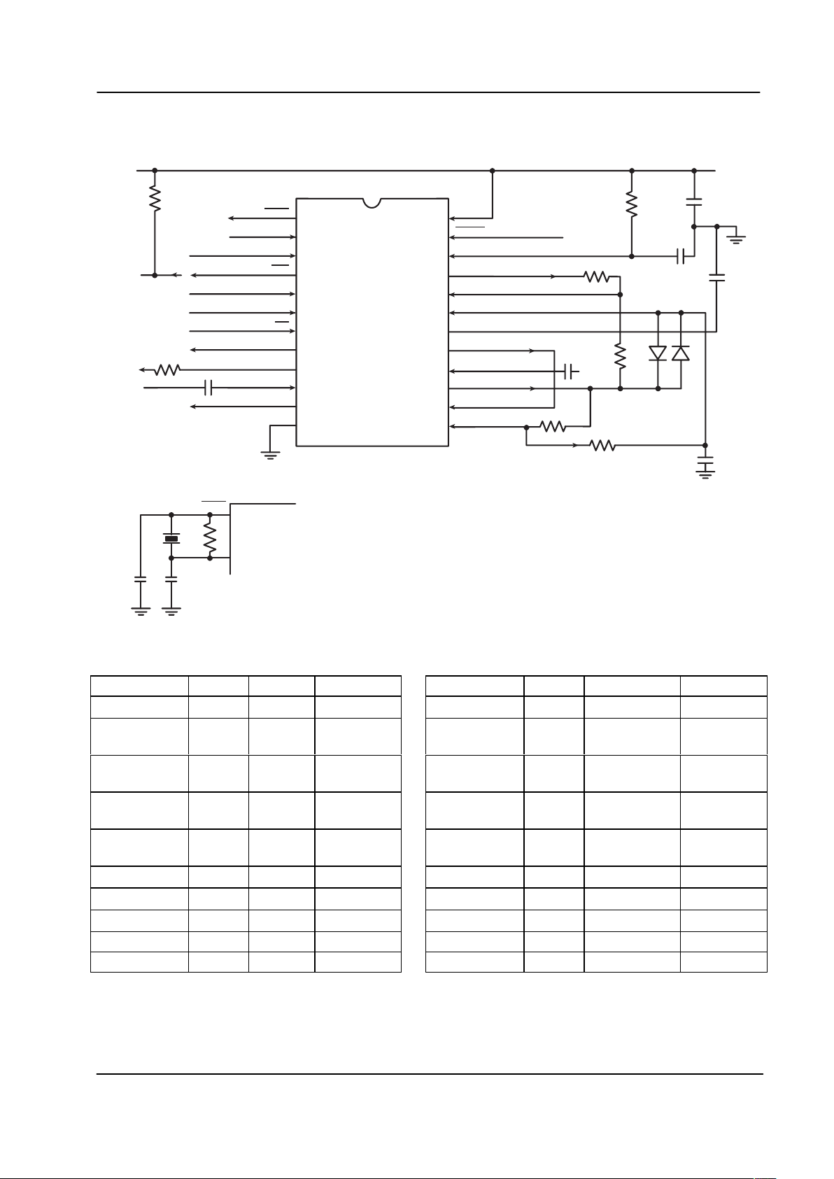
3 External Components
1
2
3
4
5
6
7
8
9
10
11
12
24
23
22
21
20
19
18
17
16
15
14
13
MX805AJ
XTAL
IRQ
CS
XTAL/CLOCK
ADDRESS SELECT
SERIAL CLOCK
COMMAND DAT A
REPL Y DA TA
TX SUB-AUDIO OUT
AUDIO IN
AUDIO OUT
BIAS
V
V
SS
V
DD
DD
WAKE
NOTONE
COMP ARATOR OUT
COMP ARATOR IN (+)
COMP ARATOR IN (-)
V
RX SUB-AUDIO OUT
RX SUB-AUDIO IN
RX AMP OUT
RX AMP IN (+)
RX AMP IN (-)
SEE INSET
C7
R8
C5
C8
C4
+
C6
+
+
R6
R4
R5
D1
D2
R3
R7
R2
C3
MX805AJ
INSET
1
2
XTAL
XTAL/CLOCK
X1 R1
C1
C2
Figure 2: Recommended External Components
Component Notes Value Tolerance Component Notes Value Tolerance
R1 5
1.0M
±5% C3
1.5F
±20%
R2 4
360k
±5% C4
15.0F,
6V Tant.
±20%
R3 1
10.0k
±5% C5
1.0F,
10V Tant.
±20%
R4 4
150k
±5% C6
1.0F,
10V Tant.
±20%
R5 4
100k
±5% C7
0.1F,
25V x 7R
±20%
R6
150k
±5% C8
1.0F
R7 6
22.0k
±5%
R8 2
360k
±5% D1 8
C1 5 D2 8
C2 5 X1 4.00MHz
Table 3: Recommended External Components

Sub-Audio Signaling Processor 8 MX805A
1998 MX-COM, Inc. www.mxcom.com Tel: 800 638 5577 336 744 5050 Fax: 336 744 5054 Doc. # 20480116.004
4800 Bethania Station Road, Winston-Salem, NC 27105-1201 USA All trademarks and service marks are held by their respective companies.
Recommended External Component Notes:
1. Xtal/Clock circuitry shown in inset are recommended in accordance with the MX-COM’s “Standard and
DBS 800 Crystal Oscillators” application note.
2. Resistor R8 is a System Component. Its value is chosen together with the MX806A Modulation Summing
Amplifier to provide a subaudio signal level of –11.0dB to the system modulator.
3. Figure 3 and Figure 4 illustrate alternative input component configurations.
4. The values for R2 and R5 are dependent on the input signal level. Values given are for the specified
composite signal (reference page 14). R4 add hysteresis to the comparator and is not always required.
5. The values used for C1 and C2 are determined by the frequency of X1.
As a guide:
5.0MHzX1 for 18pFC2C1
5.0MHzX1 for Fp332C1C
If the on-chip Xtal oscillator is to be used, then the external components X1, C1, C2, and R1 are required
as shown in Figure 2 (inset). If an external clock source is used these components are not required; the
input should be connected to the Xtal/Clock pin and the
Xtal
pin unconnected.
6. Resistor R7 is used as the DBS800 system common pull-up for the C-BUS Interrupt Request (
IRQ ) line.
The optimum value of this component will depend upon the circuitry connected to the
IRQ line.
7. The level at this point should be approximately 900mV
P-P.
8. Silicon small signal
3.1 Input Configurations
Figure 3 shows an input configuration that is generally for use for CTCSS signal and NRZ data reception.
Input coupling capacitor C3 is required because the RX Sub-Audio Input is held at V
BIAS
during all powered
conditions of the MX805A. Diodes D1 and D2 can be any silicon small signal diode.
The output resistance (open loop) of the on-chip Rx Amp is = 6k. In the configuration shown in Figure 3, the
(Rx Amp) RC time constant is therefore 90ms. If this period is too long for some systems, i.e. those using half
duplex, short data burst, and external amplifier should be considered in place of the on-chip Rx Amp.
C4
C3
D1
R3
R5
R2
R4
D2
NOTE 7
+
+
_
_
MX805A
RX AMP
MX805A
RX LPF
RX SUB-AUDIO
INPUT
D.C. RESTORATION
MX805A
COMPARAT OR
COMPARATOR
OUT
COMPARATOR IN
RX AMP IN
HYSTERESIS (OPTIONAL)
19
20
14
13
21
16
17
15
Figure 3: MX805A Input Components
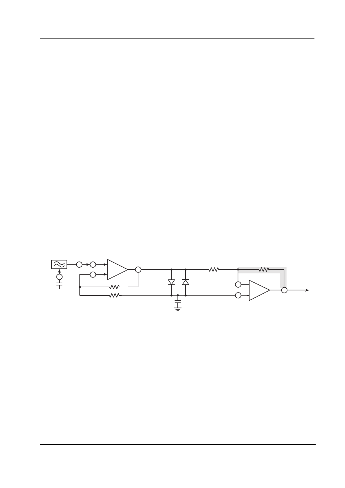
3.1.1 Using and External Op-Amp
For DC coupling the MX805A to the receiver’s discriminator output when using burst mode NRZ
communication, it is recommended that an additional, external Op-Amp is employed as configured in
Figure 4. This configuration will quickly compensate for sudden shift of DC input bas.
Components R9, R10, and R11, should be calculated to provide an accurate potential of 2.5VDC (equal to
V
BIAS
) at pin junction 15/16when using a discriminator input and 900mVP-P at the output of the external opamp. Note that the MX805A LPF has a 6dB gain. If additional filtering is required, C9 should be used, it
should be calculated with R9 to provide a lowpass cutoff frequency (f
CO
) of 500Hz.
 Loading...