

DATA BULLETIN
MX803A
Audio Signaling Processor
Features Applications
Full Duplex Audio Signaling Processor
•
Single Tone
Selective Call systems
Tone Decoder with programmable
•
NOTONE timer.
Two Individual tone encoders and a
•
programmable TX Period Timer.
Low Power CMOS Device
•
On-Chip programmable amplifier.
•
C-BUS Compatible
•
SIGNAL INPUT BIAS
(RX)
AUDIO IN
V
DD
V
BIAS
V
SS
XTAL/
CLOCK
XTAL
AUDIO SWITCH IN
CLOCK
GENERATOR
DIGITAL
NOISE
FILTER 1
PROGRAMMABLE
(TX PERIOD)
TIMER
AUDIO
SWITCH
RX FILTER
SWITCH
DIGITAL
NOISE
FILTER 2
TONE 1
GENERATOR
5-/2-TONE
DTMF 1
V
BIAS
TONE 2
GENERATOR
CUES/DTMF 2
_
+
SUMMING
AMPLIFIER
Signaling Systems supported
•
SelCall (CCIR, EEA, ZVEI I / II /III)
2-Tone SelCall
DTMF Encode
Inband Tone Signaling capability for
•
LMR and other Radio Systems.
QUALITY
METER
GATE TIME
GENERATOR
FREQUENCY
COUNTER
PROGRAMMABLE
NOTONE
TIMER
CUES
CAL
SUMMING
SWITCH
CAL/CUES
SWITCH
PRELIMINARY INFORMATION
COMMAND DAT A
REPLY DATA
C-BUS
AND
LOGIC
LOW
LOW
CHIP SELECT
INTERRUPT
SERIAL CLOCK
LOGIC INPUT
TONE 1 OUT
SUM IN
SWITCHED SUM OUT
SUM OUT
CAL/CUES OUT
TONE 2 OUT
SWITCH OUT
INTERF ACE
CONTROL
PASS
FILTER
PASS
FILTER
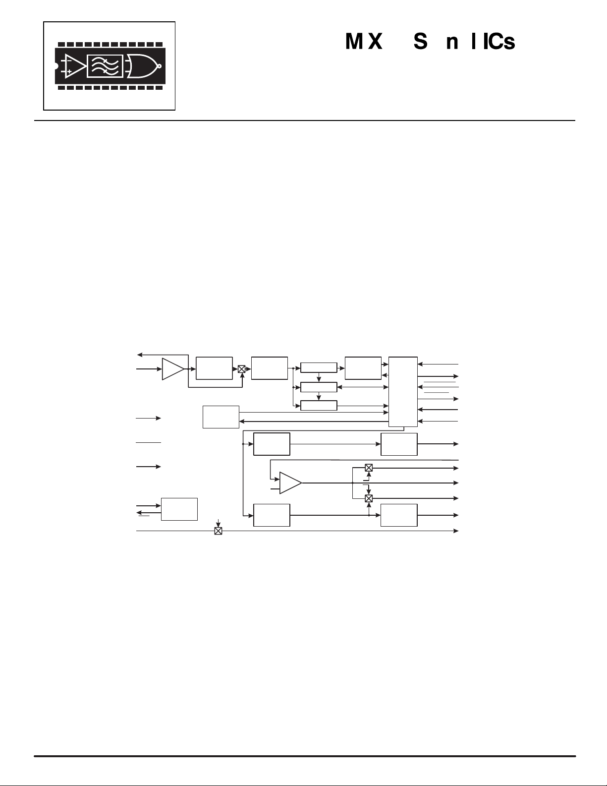
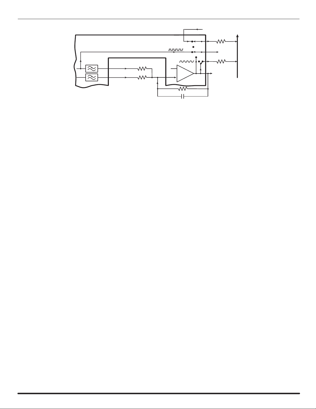
The MX803A is an audio signaling processor that provides inband tone signaling capabilities for LMR and other Radio
systems. A low-power CMOS device, the MX803A is a member of the DBS800 (Digitally integrated Baseband Subsystem) IC family (See section 4.2). Supported Signaling systems include SelCall (CCIR, EEA, ZVEI I, II, and III) 2-Tone
SelCall and DTMF encode. The use of a non-predictive decoder and a versatile encoder, allows the MX803A to operate
in any standard or non-standard tone system.
The MX803A is a full-duplex device for use with Single Tone or Selective Call systems. The MX803A consists of a tone
decoder with a programmable NOTONE timer, two individual tone encoders and a programmable TX period timer, and an
on-chip summing amplifier. Under the control of a µC, the MX803A will simultaneously encode and transmit 1 or 2 audio
tones in the 208-3000Hz range, as well as detect, decode, and indicate the frequency of any non-predicted input tone in
the frequency range of 313 to 6000Hz.
The MX803A is available in 24-pin CDIP (MX803AJ), 24-pin PLCC (MX803ALH), and 24-pin SOIC (MX803ADW)
packages.
1996 MX•COM, INC. Tele: 800 638 5577 910 744 5050 Fax: 910 744 5054 Doc. # 20480122.003

Audio Signaling Processor 2 MX803A PRELIMINARY INFORMATION
CONTENTS
Section Page
1. Block Diagram.................................................................................................................................. 3
2. Signal List......................................................................................................................................... 4
3. External Components...................................................................................................................... 6
4. General Description......................................................................................................................... 7
4.1 DESCRIPTION.......................................................................................................................................... 7
4.2 DBS800 Systems...................................................................................................................................... 7
4.3 C-BUS Control .......................................................................................................................................... 8
5. Application ....................................................................................................................................... 8
5.1 MX803A Internal Registers....................................................................................................................... 8
5.2 Address/Commands.................................................................................................................................. 9
5.3 Powersave ............................................................................................................................................... 18
5.4 Interrupt Request
5.5 Operational Recommendations................................................................................................................ 19
5.6 General Reset.......................................................................................................................................... 20
.............................................................................................................................. 19
IRQ
6. Timing Information.......................................................................................................................... 20
7. Performance Specification............................................................................................................. 22
7.1 Electrical Performance............................................................................................................................. 22
7.2 Packaging ................................................................................................................................................ 25
MX•COM, Inc. reserves the right to change specifications at any time and without notice.
1996 MX•COM, INC. Tele: 800 638 5577 910 744 5050 Fax: 910 744 5054 Doc. # 20480122.003
Audio Signaling Processor 3 MX803A PRELIMINARY INFORMATION
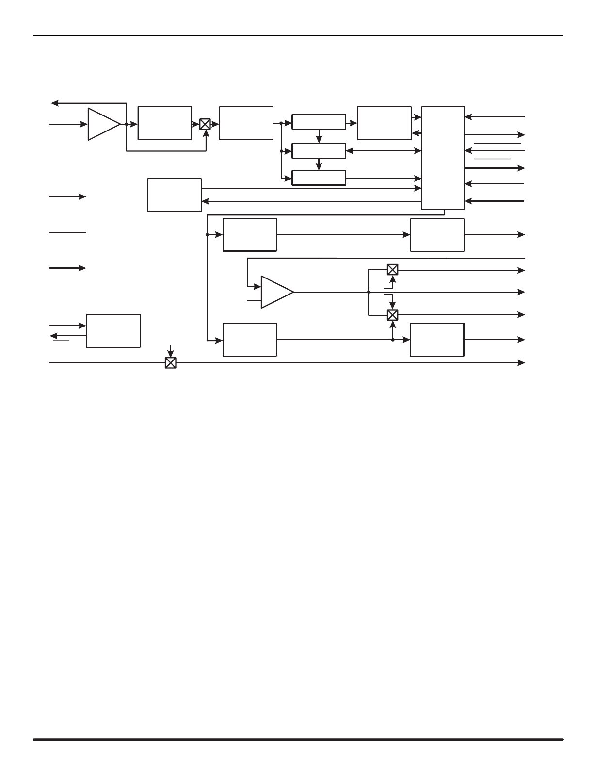
1. Block Diagram
SIGNAL INPUT BIAS
(RX)
AUDIO IN
V
DD
DIGITAL
NOISE
FILTER 1
PROGRAMMABLE
(TX PERIOD)
TIMER
RX FILTER
SWITCH
DIGITAL
NOISE
FILTER 2
QUALITY
METER
GATE TIME
GENERATOR
FREQUENCY
COUNTER
PROGRAMMABLE
NOTONE
TIMER
C-BUS
INTERFACE
AND
CONTROL
LOGIC
COMMAND DATA
REPLY DATA
CHIP SELECT
INTERRUPT
SERIAL CLOCK
LOGIC INPUT
V
BIAS
V
SS
XTAL/
CLOCK
CLOCK
GENERATOR
XTAL
AUDIO SWITCH IN
AUDIO
SWITCH
TONE 1
GENERATOR
5-/2-TONE
DTMF 1
_
V
BIAS
+
SUMMING
AMPLIFIER
TONE 2
GENERATOR
CUES/DTMF 2
Figure 1: Block Diagram
CUES
CAL
SUMMING
SWITCH
CAL/CUES
SWITCH
LOW
PAS S
FILTER
LOW
PAS S
FILTER
TONE 1 OUT
SUM IN
SWITCHED SUM OUT
SUM OUT
CAL/CUES OUT
TONE 2 OUT
SWITCH OUT
1996 MX•COM, INC. Tele: 800 638 5577 910 744 5050 Fax: 910 744 5054 Doc. # 20480122.003
Audio Signaling Processor 4 MX803A PRELIMINARY INFORMATION
2. Signal List
Pin No. Name Type Description
1
XTAL
2 Xtal/Clock Input Input to the on-chip clock oscillator inverter. A Xtal or externally derived clock
3 Reply Data Output
4
CS
5 Command Data Input
6 Logic Input Input This “real-time” input is available as a general purpose logic input port which
7
IRQ
10 Audio Switch In Input Input to the stand-alone on-chip Audio Switch. This function is
11 Audio Switch Out Output Output of the stand-alone on-chip Audio Switch..
12 V
SS
13 Rx Audio In Input Received audio tone signaling input. This input must be ac coupled and
14 Signal Input Bias Input External components are required between this input and the RX Audio In pin.
15 V
BIAS
16 Tone 1 Out Output Tone 1 Generator (2-/5-tone Selcall or DTMF 1) output. External gain and
17 Tone 2 Out Output Tone 2 Generator (2-/5-tone Selcall, CUES or DTMF 2) output. External gain
Output Output of the on-chip clock oscillator. External components are required at this
output when a Xtal is used. See Figure 2.
should be connected here. See Figure 2.
C-BUS serial data output to the µC. The transmission of Reply Data bytes is
synchronized to the Serial Clock under the control of the Chip Select input.
This 3-state output is held at high impedance when not sending data to the µC.
See Figure 8 and Figure 9.
Input
C-BUS data loading control function. This input is provided by the µC. Data
transfer sequences are initiated, completed or aborted by the chip select signal.
See Figure 8 and Figure 9.
C-BUS serial data input from the µC. Data is loaded to this device in 8-bit
bytes, MSB (B7) first and LSB (B0) last, synchronized to the Serial Clock. See
Figure 8 and Figure 9.
can be read from the Status Register. See Table 3.
G/Purpose Timer Period Expired
NOTONE Timer Period Expired
RX Tone Measurement Complete
These interrupts are inactive during relevant powersave conditions and can be
disabled by bits 5 and 6 in the Control Register.
Output
Output of this pin indicates an interrupt condition to the µC by going to a logic
“0.” This is a “wire-or-able” output, allowing the connection of up to 8
peripherals to 1 interrupt port on the µC. This pin has a low impedance
pulldown to logic “0” when active and a high impedance when inactive. The
system IRQ line requires one pullup resistor to V
. The conditions that cause
DD
interrupts are indicated in the Status Register and are shown below:
enabled/disabled by Bit 7 of the Control Register
Power Negative supply (GND).
connected, using external components, to the Signal Input Bias pin. See Figure
2.
See Figure 2.
Output Internal circuitry bias signal, held at VDD/2. This pin should be decoupled to V
SS
by capacitor C2. See Figure 2..
coupling components are required at this output when operating in a complete
DBS 800 audio installation. The frequency of this output is determined by
writing to the TX Tone Generator 1 Register (Table 5). See Figure 2.
and coupling components are required at this output when operating in a
complete DBS 800 audio installation. The frequency of this output is
determined by writing to the TX Tone Generator 2 Register (Table 5).
See Figure 2.
1996 MX•COM, INC. Tele: 800 638 5577 910 744 5050 Fax: 910 744 5054 Doc. # 20480122.003

Audio Signaling Processor 5 MX803A PRELIMINARY INFORMATION
Pin No. Name Type Description
18 CAL/CUES Out Output An auxiliary, selectable tone frequency output, providing a square wave
CALibration signal from the Tone 2 Generator or a sine wave CUES (beep)
signal from the Summing Amplifier. The output mode (CAL or CUES) is
selected by Bit 14 in the TX Tone Generator 2 Register (Table 5). When Tone
Generator 2 is set to Notone, the CAL input is pulled to V
powersave of Tone Generator 2 it is held at V
SS
.
; during a
BIAS
19 Sum in Input Input to the on-chip Summing Amplifier. This amplifier is available for
combining Tone 1 and Tone 2 outputs (DTMF). Gain and coupling components
should be used at this input to provide the required system gains. See Figure 2
and Figure 3
20 Sum Out Output Output of the on-chip summing amplifier. Combined tones (1 and 2) are
available at this output. See Figure 2 and Figure 3.
21 Switched Sum
Out
Output This is the combined tone output available for transmitter modulation. The
switch allows control of the MX803A output. Control of this switch is by Bit 4 of
the Control Register. See Figure 2 and Figure 3.
23 Serial Clock Input
C-BUS serial clock input. This clock, produced by the µC, is used for transfer
timing of commands and data to and from the MX803A. See Figure 8 and
Figure 9.
24 V
DD
Power Positive supply. A single +5 volt power supply is required. Levels and voltages
within this Audio Signaling Processor are dependent upon this supply..
8, 9, 22 N/C No Internal Connection. These pins may be connected to VSS to improve
screening and reduce noise levels around the MX803A.
1996 MX•COM, INC. Tele: 800 638 5577 910 744 5050 Fax: 910 744 5054 Doc. # 20480122.003
Audio Signaling Processor 6 MX803A PRELIMINARY INFORMATION
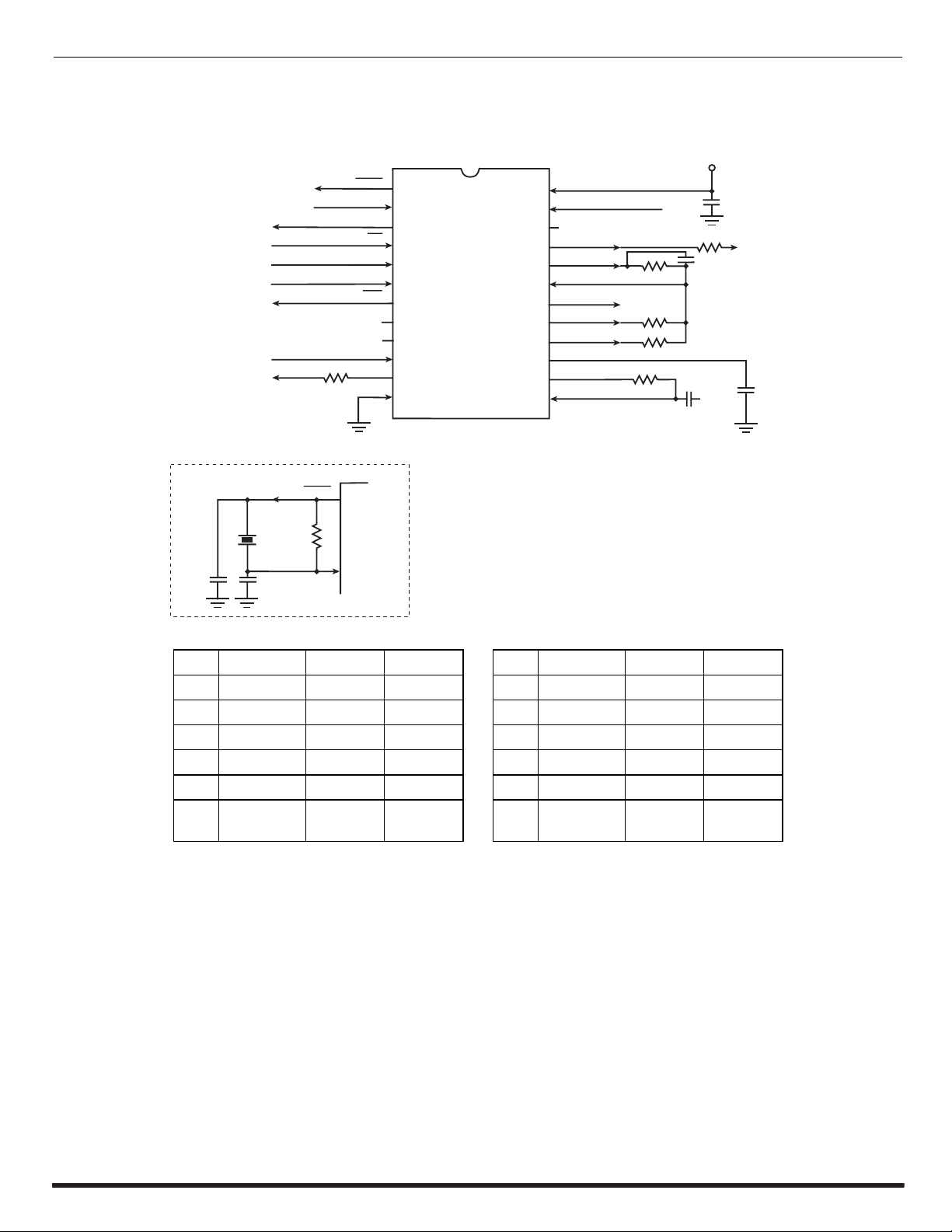
3. External Components
V
DD
V
SEE INSET
BELOW
XTAL/CLOCK
REPLY DATA
COMMAND DATA
LOGIC INPUT
AUDIO SWITCH IN
AUDIO SWITCH OUT
R
7
XTAL
CS
IRQ
V
1
2
3
4
5
6
MX803A
7
8
9
10
11
SS
12
BIAS
24
SERIAL CLOCK
23
22
SWITCHED SUM OUT
21
SUM OUT
20
SUM IN
19
CAL/CUES OUT
18
TONE 2 OUT
17
TONE 1 OUT
16
V
BIAS
15
SIGNAL BIAS
14
RX AUDIO IN
13
C
6
R
6
C
R
4
R
5
R
2
5
TONE LEVEL
AND GAIN
COMPONENTS
C
1
C
2
R
3
INSET
C
4
C
R1
R2
R3 Note 2, 3
R4 Note 2, 3
R5 Note 2, 3
R6 Note 2
R7 Note 2, 5
R
X
1
XTAL/CLOCK
3
XTAL
1
1.0M
2.0M
100k
82.0k
122k
100k
100k
1
MX803A
2
Ω
Ω
Ω
Ω
Ω
Ω
Ω
±10% C1
±10% C2
0.1µF
1.0µF
±20%
±20%
±10% C3 Note 4 33.0pF ±20%
±10% C4 Note 4 33.0pF ±20%
±10% C5 Note 3 22.0pF ±20%
±10% C6
1.0µF
±20%
±10% X1 Note 1, 4 4.00MH
z
Figure 2: Recommended External Components
Notes:
1. Xtal/clock components described are recommended in accordance with MX-COM's Application Note on Standard and
DBS 800 Crystal Oscillator Circuits (April 1990). For best results, a crystal oscillator design should drive the clock
inverter input with signal levels of at least 40% of V
, peak to peak. Tuning fork crystals generally cannot meet this
DD
requirement. To obtain crystal oscillator design assistance, consult your crystal manufacturer.
2. System Components whose values are calculated to allow the MX803A to operate with other DBS 800 microcircuits.
Figure 3 shows these components used in the system signal paths.
3. R3, R4, R5 and C5 are tone mixing components calculated to provide a 3dB tone differential (twist) for use in a DTMF
configuration. Single tone output levels are set independently.
4. When X1 > 5.00MHz, C3 = C4 = 18pF
5. R7 provides modulation level and matching outputs for the MX803A.
1996 MX•COM, INC. Tele: 800 638 5577 910 744 5050 Fax: 910 744 5054 Doc. # 20480122.003
Audio Signaling Processor 7 MX803A PRELIMINARY INFORMATION
FROM MX806A
CUES
MAIN PROCESS OUT
AUDIO SWITCH OUT
11
18
CAL/CUES OUT
21
SWITCHED SUM OUT
SUM OUT
20
AUDIO SWITCH IN
MX803A
TONE 2 OUT
17
16
TONE 1 OUT
Figure 3: Example of Signal Switching in a DBS800 microcircuit
SUM IN
BIAS
19
10
+
_
CAL
SUMMING
AMPLIFIER
TO MX806A
CALIBRATION IN
TO MX806A
SUM IN
DBS 800 TRANSMIT A UDIO BUS
4. General Description
4.1 DESCRIPTION
The MX803A is an audio signaling processor that provides inband tone signaling capabilities for LMR and other Radio
systems. A low-power CMOS device, the MX803A is a member of the DBS800 (Digitally integrated Baseband Subsystem) IC family (See section 4.2). Supported Signaling systems include SelCall (CCIR, EEA, ZVEI I, II, and III) 2-Tone
SelCall and DTMF encode. The use of a non-predictive decoder and a versatile encoder, allows the MX803A to operate
in any standard or non-standard tone system.
The MX803A is a full-duplex device for use with Single Tone or Selective Call systems. The MX803A consists of a tone
decoder with a programmable NOTONE timer, two individual tone encoders and a programmable TX period timer, and an
on-chip summing amplifier. Under the control of a µC, the MX803A will simultaneously encode and transmit 1 or 2 audio
tones in the 208-3000Hz range, as well as detect, decode, and indicate the frequency of any non-predicted input tone in
the frequency range of 313 to 6000Hz.
A general purpose logic input, interfacing directly with the Status Register, is provided. This may be used as an auxiliary
method of routing digital information to the µC via C-BUS. Output frequencies are produced from data loaded to the
MX803A. A programmable, general purpose, on-chip timer sets the tone transmit periods. A Dual-Tone Multi-Frequency
(DTMF) output is obtained by combining the 2 independent output frequencies in the integral summing amplifier. This
process can also be used for level correction.
Tones produced by the MX803A can be used in the system as modulation calibration inputs and as “CUE” audio
indications to the operator. Received tones are measured and their frequency indicated to the µC in the form of a
received data word. A poor quality or incoherent tone will indicate Notone.
4.2 DBS800 Systems
The Digitally-Integrated Baseband Subsystem (DBS800) is a family of low power ICs which provide a comprehensive
range of audio processing and signaling functions for use within LMR and other Radio Systems. Each DBS800 IC may
be used as part of a complete audio system, or each IC may operate as a stand alone. The system and ICs are
partitioned in such a way that radio designers can easily select the device or devices appropriate to their needs.
The DBS800 family consists of the following ICs:
4.2.1 MX802 DVSR Codec
This is a full-duplex CVSD speech encoder/decoder with the ability to store and retrieve data within attached DRAM
(Dynamic Random Access Memory) using an on-chip DRAM controller. The MX802 also provides on-chip input and
output audio filtering.
4.2.2 MX803A Audio Signaling Processor
This provides an inband tone signaling ability to LMR and other Radio Systems.
1996 MX•COM, INC. Tele: 800 638 5577 910 744 5050 Fax: 910 744 5054 Doc. # 20480122.003
Audio Signaling Processor 8 MX803A PRELIMINARY INFORMATION
4.2.3 MX805A Sub-Audio Signaling Processor
This provides a sub-audio and digital signaling (NRZ) ability to LMR and other Radio Systems.
4.2.4 MX806A Audio Processor
This is a half duplex audio processor providing all DBS800 system audio signal conditioning and filtering capabilities for
the system transmit and receive paths.
4.2.5 MX809 MSK Modem
This is an intelligent, half-duplex 1200bps MSK/FFSK Modem with software programmable byte-synchronization system
and checksum generation and checking.
4.2.6 MX812 VSR Codec
This is a half-duplex CVSD speech encoder/decoder with the ability to store and retrieve data within attached DRAM
(Dynamic Random Access Memory) using an on-chip DRAM controller
4.3 C-BUS Control
C-BUS is the controlling hardware and software interface for all members of the DBS800 family. It enables the serial, bidirectional transfer of commands and data throughout the system, allowing total flexibility of operational control and data
handling. System upgrades can be achieved by a simple software or firmware change.
The C-BUS physically consist of 5 lines. These lines are Serial Clock, Command Data, Reply Data, Chip Select (
and Interrupt Request (
). A description of each may be found in section 2.
IRQ
CS),
5. Application
Control of the MX803A Audio Signaling Processor's operation is by communication between the µC and the MX803A
internal registers on the C-BUS using Address/Commands (A/Cs) and appended instructions or data. See Figure 8. The
use and content of these instructions is detailed in the following sections.
For additional application information contact MX•COM, Inc.
5.1 MX803A Internal Registers
Write only, control and configuration of the MX803A.
Control Register
Status Register
RX Tone Frequency Register
RX Notone Timer
TX Tone Generator 1 Register
TX Tone Generator 2 Register
General Purpose Timer Register
30
H
Read only, reporting of device functions.
31
H
Read only, indicates frequency of the last received input.
32
H
Write only, setting of the RX Notone period.
33
H
Write only, setting the required output frequency from TX Tone Generator 1.
34
H
Write only, setting the required output frequency from TX Tone Generator 2.
35
H
Write only, setting of a general purpose sequential time period.
36
H
1996 MX•COM, INC. Tele: 800 638 5577 910 744 5050 Fax: 910 744 5054 Doc. # 20480122.003
 Loading...