MX COM Inc MX802J, MX802LH, MX802LH8 Datasheet
DATA BULLETIN
MX802
DVSR CODEC
Features Applications
DVSR (Data/Voice Storage and Retrieval)
Codec
CVSD Codec Encoder and Decoder
Control and Timing Circuitry for 4Mbits
of external DRAM
Low Power Operation
Member of DBS800 Family (C-BUS
Compatible)
SERIAL
CLOCK
COMMAND
DATA
C-BUS INTERFA CE AND CONTR OL LOGIC
REPLY
DATA
Answering Machines where an incoming
speech message is stored for later recall
Busy Buffering, in which an outgoing
speech message is stored temporarily
Automatic transmission of pre-recorded
alarm or status messages.
Time Domain Scrambling of Speech
messages
VOX control of transmitter functions
Temporary Data Storage, such as
buffering of over-air data transmissions
XTAL/
CLOCK
CLOCK
GENERATOR
XTAL
IRQCS
AUDIO
IN
AUDIO
OUT
STATUS
REGISTER
ENCODE
OUT)
CLOCK
DRAM Data Out/
A1/DEI
(DECODER
POWER
ASSESS
DECODER
CLOCK
DIRECT ACCESS CLOCKS AND DATA
DRAM Data In/
A0/ENO
(ENCODER
A2/DCKA3/ECKA4A5A6A7A8A9
DECODE
CLOCK
PA TTERN
V
IN)
DD
DEMODMOD
IDLE
V
V
SS
BIAS
DATA
READ
COUNTER
WE
CAS
WRITE
COUNTER
RAS1 RAS2
PLAY
COMMAND
BUFFER
DATA
SPEECH
PLAY
COUNTERS
DRAM CONTROL AND TIMING
RAS4
RAS3
STORE
COMMAND
BUFFER
SPEECH
STORE
COUNTERS
CONTROL
REGISTER
ENCODER
CLOCK
DRAM ADDRESS LINES
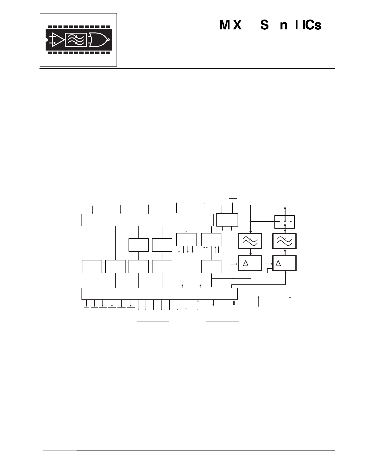
The MX802 Data/Voice Storage and Retrieval (DVSR) Codec contains a Continuously Variable Slope Delta
Modulation (CVSD) encoder and decoder as well as control and timing circuitry for up to 4Mbits of external
DRAM. As a member of the DBS800 series, it also contains interface and control logic for the “C-BUS” serial
interface.
When used with external DRAM, theMX802 had four primary functions: Speech Storage, Speech layback,
Data Storage, and Data Retrieval. The Speech Storage and Playback may be performed concurrently with
data storage or retrieval.
On-chip the Delta Codec is supported by input and output analog switched-capacitor filters and audio output
switching circuitry. The DRAM control and timing circuitry provides all the necessary address, control, and
refresh signals to interface to external DRAM.
The MX802 may also be used without DRAM (as a “stand alone” CVSD Codec), in which case direct access
is provided to the CVSD Codec digital data and clock signals. All signals are controlled by “C-BUS”
commands from the system microcontroller.
The MX802 may be used with a 5.0V power supply and is available in the following packages:
24-pin PLCC (MX802LH), 28-pin PLCC (MX802LH8), and 28-pin PDIP (MX802P).
1998 MX-COM, Inc. www.mxcom.com Tel: 800 638 5577 336 744 5050 Fax: 336 744 5054 Doc. # 20480033.008
4800 Bethania Station Road, Winston-Salem, NC 27105-1201 USA All trademarks and service marks are held by their respective companies.

DVSR CODEC 2 MX802
Contents
Section Page
1 Block Diagram................................................................................................................3
2 Signal List.......................................................................................................................4
3 External Components....................................................................................................6
4 General Description.......................................................................................................7
4.1 Controlling Protocol ............................................................................................................. 8
4.1.1 Address/Commands...............................................................................................................8
4.1.2 Operation with DRAM.............................................................................................................8
4.1.3 Speech...................................................................................................................................9
4.1.4 Data Handling.......................................................................................................................10
4.2 Write to Control Register ................................................................................................... 12
4.2.1 General Reset......................................................................................................................12
4.2.2 Direct Access .......................................................................................................................12
4.2.3 Play Counter.........................................................................................................................12
4.2.4 DRAM Control......................................................................................................................12
4.2.5 Codec Powersave................................................................................................................12
4.2.6 Command Interrupt Enable.................................................................................................. 12
4.2.7 Store and Play Speech Synchronization..............................................................................12
4.2.8 Decoder and Encoder Control..............................................................................................12
4.3 Encoder and Decoder Control : Analog Input and Output Control..................................... 14
4.3.1 Time Compression of Speech..............................................................................................15
4.4 Read Status Register ........................................................................................................ 15
4.4.1 Interrupts..............................................................................................................................15
4.4.2 Power Register.....................................................................................................................15
5 Application – Codec Performance .............................................................................17
6 Performance Specifications........................................................................................19
6.1 Electrical Specifications..................................................................................................... 19
6.1.1 Absolute Maximum Limits ....................................................................................................19
6.1.2 Operating Limits...................................................................................................................19
6.1.3 Operating Characteristics.....................................................................................................20
6.1.4 Timing...................................................................................................................................21
6.2 Packages........................................................................................................................... 23
MXCOM, Inc. reserves the right to change specifications at any time without notice.
1998 MX-COM, Inc. www.mxcom.com Tel: 800 638 5577 336 744 5050 Fax: 336 744 5054 Doc. # 20480033.008
4800 Bethania Station Road, Winston-Salem, NC 27105-1201 USA All trademarks and service marks are held by their respective companies.
DVSR CODEC 3 MX802
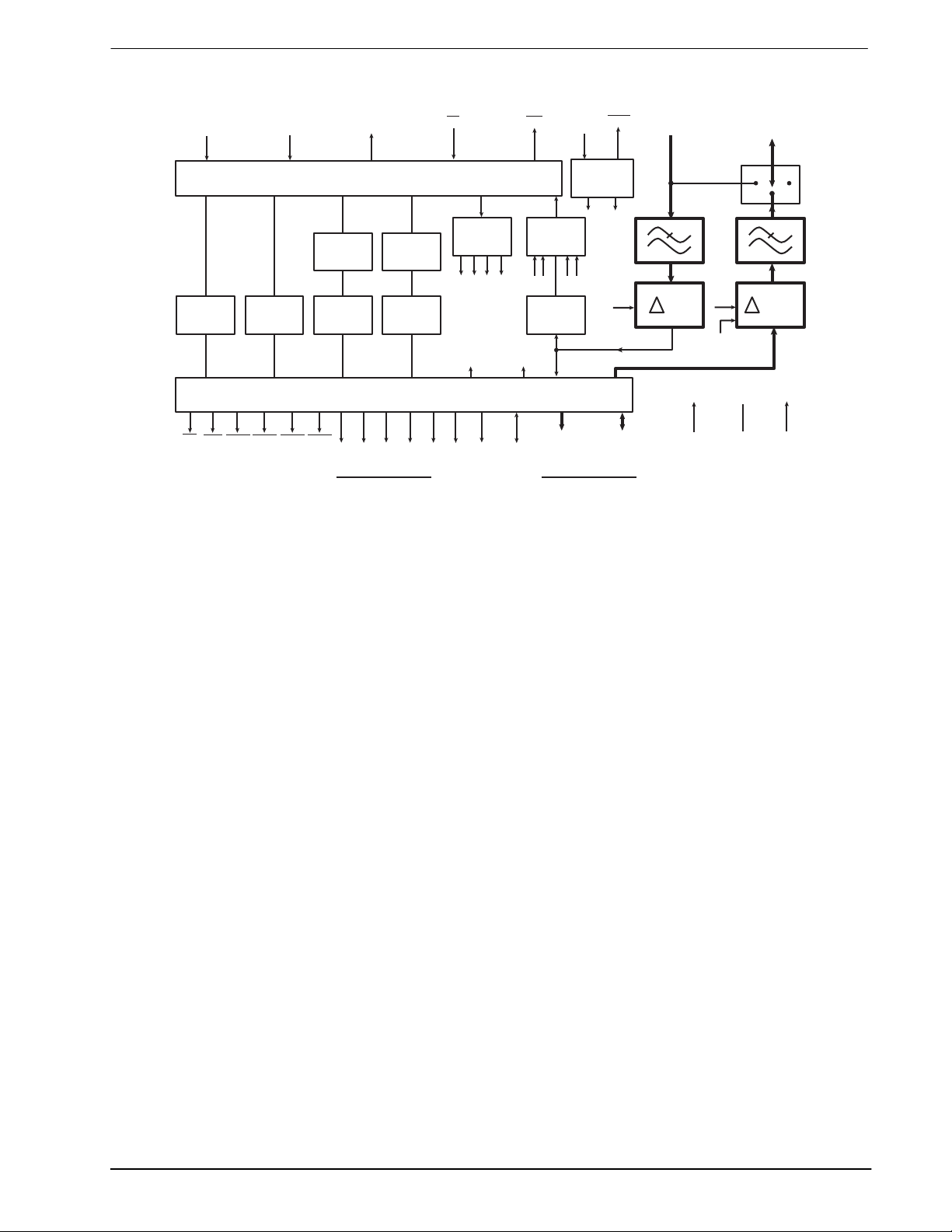
1 Block Diagram
SERIAL
CLOCK
COMMAND
DATA
REPLY
DATA
C-BUS INTERFACE AND CONTROL LOGIC
DATA
READ
COUNTER
WE
CAS
DATA
WRITE
COUNTER
RAS1 RAS2
PLAY
COMMAND
BUFFER
SPEECH
PLAY
COUNTERS
DRAM CONTROL AND TIMING
RAS4
RAS3
STORE
COMMAND
BUFFER
SPEECH
STORE
COUNTERS
Figure 1: Block Diagram
IRQCS
CONTROL
REGISTER
ENCODER
DRAM ADDRESS LINES
DECODER
CLOCK
CLOCK
DIRECT ACCESS CLOCKS AND DATA
A2/DCKA3/ECKA4A5A6A7A8A9
STATUS
REGISTER
POWER
ASSESS
DRAM Data In/
A0/ENO
(ENCODER
OUT)
XTAL/
CLOCK
CLOCK
GENERATOR
ENCODE
CLOCK
DRAM Data Out/
XTAL
A1/DEI
(DECODER
IN)
AUDIO
IN
AUDIO
OUT
DECODE
CLOCK
IDLE
PATTERN
V
DD
V
BIAS
DEMODMOD
V
SS
1998 MX-COM, Inc. www.mxcom.com Tel: 800 638 5577 336 744 5050 Fax: 336 744 5054 Doc. # 20480033.008
4800 Bethania Station Road, Winston-Salem, NC 27105-1201 USA All trademarks and service marks are held by their respective companies.
DVSR CODEC 4 MX802
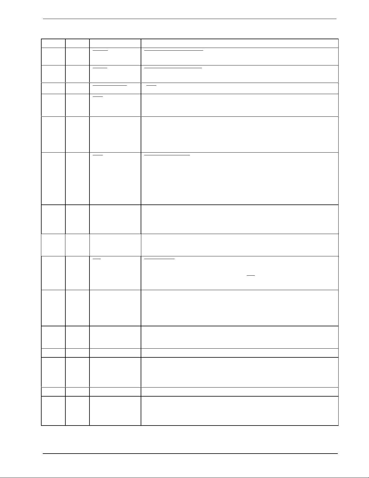
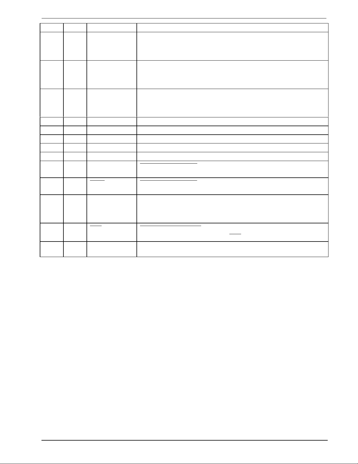
2 Signal List
J/LH8 LH Signal Description
1
RAS2
Address Strobe input of the second 1Mbit DRAM chip (if used).
21
RAS1
Address Strobe input of the first DRAM chip.
32
4
Xtal
Enable Write
( EW ) The DRAM of Read/Write control pin.
This is the output of the 4.0MHz on –chip clock oscillator. External
components are required at the output when a Xtal is used. A Xtal
cannot be used with the 24-pin version.
5 3 Xtal/Clock This is the input to the on-chip clock oscillator inverter. A 4.0MHz Xtal
or externally derived clock should be connected here. See Figure 2.
This clock provides timing for on-chip elements, filters, etc. A Xtal
cannot be used with the 24-pin version. Various Xtal frequencies can
be used with this device. See Table 5 for Sampling Rate Variations.
64
IRQ
Request Interrupt The output of this pin indicates an interrupt condition
to the microcontroller by going to logic’0’. This ‘wire-or able’ output,
enabling the connection of up to 8 peripherals to 1 interrupt port on the
microcontroller. This pin is an open drain output. It therefore has a low
impedance pulldown to logic ‘0’ when active and a high impedance
when inactive. Conditions indicated by this function are Power Reading
Ready, Play Command Complete, and Store Command Complete.
7 5 Serial Clock This is the C-BUS serial clock input. This clock, produced by the
microcontroller, is used to transfer timing commands and data to and
from the DVSR Codec. See timing diagrams. Clock requirements vary
for different MX802 functions.
8 6 Command Data
This is the C-BUS serial data input from the microcontroller. Data is
loaded to this device in 8-bit bytes, MSB (bit 7) first, and LSB (bit 0) last,
synchronized to the Serial clock. See Timing diagrams.
97
CS
Select Chip : The C-BUS data transfer control function, this input is
provided by the microcontroller. Command Data transfer sequences are
initiated, completed, or aborted by the
Diagrams.
10 8 Reply Data
This is the C-BUS serial data output to the microcontroller. The
transmission of Reply Data bytes is synchronized to the Serial Data
Clock under the control of the Chip Select input. This 3-state output s
held at high impedance when not sending data to the microcontroller.
See Timing diagrams.
11 9 V
BIAS
This is the output of the on-chip analog circuitry bias system, held
internally at V
DD
C1. See Figure 2.
12 10 Audio Out This is the Analog signal out.
13 11 Audio In
This is the audio (speech) input. The signal to this pin must be AC
coupled by capacitor C4 and decoupled to V
optimum noise performance this input should be driven from a source
impedance of less than 100.
14 12 V
SS
15 13 Encoder Out
(ENO)
Negative Supply (GND)
DRAM Data In/A0/Direct Access -- This is connected to the DRAM data
input and address line A0. With no DRAM used, this output is available
in a Direct Access mode as the Delta Encoder digital data Output.
Direct Access control is achieved by Control Register byte 1, bit 7.
This pin should be connected to the Row
2 Strobe sRow Addres
1 Strobe sRow Addres This pin should be connected to the Row
CSsignal. See Timing
/2. This pin should be decoupled to VSS by capacitor
by HF capacitor C6. For
SS
1998 MX-COM, Inc. www.mxcom.com Tel: 800 638 5577 336 744 5050 Fax: 336 744 5054 Doc. # 20480033.008
4800 Bethania Station Road, Winston-Salem, NC 27105-1201 USA All trademarks and service marks are held by their respective companies.
DVSR CODEC 5 MX802
J/LH8 LH Signal Description
16 14 Decoder In (DEI)
DRAM Data Out/A1/Direct Access --: This is connected to the DRAM
data output and address line A1. With no DRAM used, this pin is
available in a Direct Access mode as the Delta Decoder Clock input.
Direct Access control is achieved by Control Register byte 1, bit 6.
17 15 Decoder Clock
(DCK):
DRAM A2/Direct Access -- This is the DRAM address line A2. With no
DRAM employed, this pin is available in a Direct Access mode as the
Delta Decoder Clock Input. Direct Access control is achieved by Control
Register byte 1, bit 6.
18 16
Encoder Clock
(ECK)
DRAM A3/Direct Access: This is the DRAM address line A3. With no
DRAM employed, this pin is available in a Direct Access mode as the
Delta Encoder Clock Output. Direct Access control is achieved by
Control Register byte1, bit 6.
19 17 DRAM A4 DRAM address line 4.
20 18 DRAM A5 DRAM address line 5.
21 19 DRAM A6 DRAM address line 6.
22 20 DRAM A7 DRAM address line 7.
23 21 DRAM A8 DRAM address line 8.
24 RAS4
4 Strobe sRow Addres : This pin should be connected to the Row
Address Strobe input of the fourth 1Mbit DRAM chip (if used).
25
3RAS 3 Strobe sRow Addres : This pin should be connected to the Row
Address Strobe input of the third 1Mbit DRAM chip (if used).
26 22 DRAM A9
This is DRAM address line A9. This pin is not connected when a
256kbit DRAM is used. Note: To simplify PCB layout, the DRAM
address inputs A0-A8 may be connected in any physical order to the
DVSR Codec output pins A0-A8.
27 23
28 24 V
CAS Strobe AddressColumn : This is the DRAM Column Address Strobe
DD
pin. It should be connected to the
Positive supply. A single, stable +5 volt supply is required. Levels and
CASpins of all DRAM chips.
voltages within the DVSR Codec are dependent upon this supply.
Table 1: Signal List
1998 MX-COM, Inc. www.mxcom.com Tel: 800 638 5577 336 744 5050 Fax: 336 744 5054 Doc. # 20480033.008
4800 Bethania Station Road, Winston-Salem, NC 27105-1201 USA All trademarks and service marks are held by their respective companies.
DVSR CODEC 6 MX802
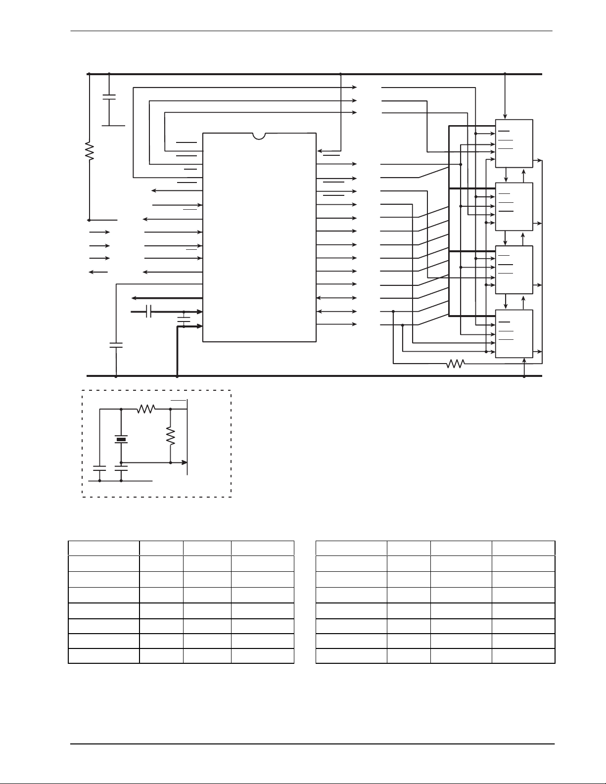
3 External Components
V
DD
C
V
SS
R
1
SEE INSET
C-BUS
INTERFACE
5
RAS2
RAS1
XT AL
XT AL/CLOCK
SERIAL CLOCK
COMMAND DAT A
REPLY DATA
AUDIO OUT
AUDIO IN
C
6
C
4
C
1
WE
IRQ
V
BIAS
V
CS
V
DD
1
*
2
3
4
*
5
6
7
MX802J
8
9
10
11
12
13
14
SS
V
SS
28
CAS
27
A9
26
RAS3
25
*
*
24
23
22
21
20
19
18
17
16
15
RAS4
A8
A7
A6
A5
A4
A3/ECK
A2/DCK
A1/DEI
A0/ENO
R
4
4X1Mbit
DRAM
A0 - A9
WE
CAS
RAS
D
A0 - A9
WE
CAS
RAS
D
A0 - A9
WE
CAS
RAS
D
A0 - A9
WE
CAS
RAS
D
Q
Q
Q
Q
INSET
C
3
X
1
C
2
XTAL
R
3
R
2
XTAL/CLOCK
V
SS
4
*
MX802J
5
Figure 2: Recommended External Components
Component Notes Value Tolerance Component Notes Value Tolerance
R1
R2
22.0k
1.0M
R3 1 ±10% C6
R4
1.0k
±5% C4 1.0µF ±20%
±10% C5 1.0µF ±20%
.001F
±20%
±10%
C1 1.0µF ±10% X1 4.00MHz
C2 33.0pF ±20% X1 4.032MHz
C3 33.0pF ±20% X1 4.096MHz
Table 2: Recommended External Components
1998 MX-COM, Inc. www.mxcom.com Tel: 800 638 5577 336 744 5050 Fax: 336 744 5054 Doc. # 20480033.008
4800 Bethania Station Road, Winston-Salem, NC 27105-1201 USA All trademarks and service marks are held by their respective companies.

DVSR CODEC 7 MX802
Recommended External Component Notes:
1. Xtal circuitry shown in inset is in accordance with the MX-COM Standard and DBS 800 Crystal
Application Note.
2. External Xtal circuitry is not applicable to the 24-pin/lead version of this device. Only an externally
derived clock input can be used.
3. Functions whose pins are marked with and asterisk (*) in Figure 2 are not available on the 24-pin/lead
versions of this device. Pin numbers illustrated are for 28-pin versions.
4. Table 5 details the actual encoder/decoder sample rates available using the Xtal frequencies
recommended above.
5. Resistor R1 is used as the DBS800 system common pull-up for the C-BUS Interrupt Request
The optimum value will depend on the circuitry connected to the
IRQ . Up to 8 peripherals may be
IRQ
line.
connected to this line.
6. Recommended DRAM parameters:
256kbit x 1 or 1Mbit x 1 Dynamic Random Access Memory with
"RAS before CAS" refresh mode.
Maximum Row address time = .200us.
Example DRAM types:
256kbit (262,144 bits)
Texas Instruments (TMS4256-20)
Hitachi (HM51256-15)
1Mbit (1,048,576 bits)
Texas Instruments (TMS4C1024-15)
Hitachi (HM511000-15)
7. Figure 2 shows connections to 4x1 Mbit sections of DRAM. If desired, to simplify PCB layout, the DRAM
inputs A0-A8 may be connected in any order to the MX802 DVSR Codec output pins A0-A8.
Connections to 256kbit DRAM are similar, but A9 I left unconnected.
8. When using the MX802 “stand alone” 9Direct Access), no DRAM sections should be connected.
4 General Description
The MX802 Data/Voice Storage and Retrieval (DVSR) Codec contains a Continuously Variable Slope Delta
Modulation (CVSD) encoder and decoder as well as control and timing circuitry for up to 4Mbits of external
DRAM. As a member of the DBS800 series, it also contains interface and control logic for the “C-BUS” serial
interface.
When used with external DRAM, theMX802 had four primary functions: Speech Storage, Speech layback,
Data Storage, and Data Retrieval. The Speech Storage and Playback may be performed concurrently with
data storage or retrieval.
Speech Storage:
Speech signals present at the Audio Input may be digitized by the CVSD encoder. The
resulting bit stream is stored in DRAM. This process also provides readings of the
speech signal power level. These readings are used by the system microcontroller for
pause reduction.
Speech Playback:
Digitized speech may be read from DRAM and converted back into analog from by the
CVSD decoder.
Data Storage:
Digital data derived via the C-BUS from the Modem or system data may be stored in
DRAM.
Data Playback:
Digital data may be read from DRAM and sent over the C-BUS to the system
microcontroller.
On-chip the Delta Codec is supported by input and output analog switched-capacitor filters and audio output
switching circuitry. The DRAM control and timing circuitry provides all the necessary address, control, and
refresh signals to interface to external DRAM.
The MX802 may also be used without DRAM (as a “stand alone” CVSD Codec), in which case direct access
is provided to the CVSD Codec digital data and clock signals. All signals are controlled by “C-BUS”
commands from the system microcontroller.
1998 MX-COM, Inc. www.mxcom.com Tel: 800 638 5577 336 744 5050 Fax: 336 744 5054 Doc. # 20480033.008
4800 Bethania Station Road, Winston-Salem, NC 27105-1201 USA All trademarks and service marks are held by their respective companies.
DVSR CODEC 8 MX802
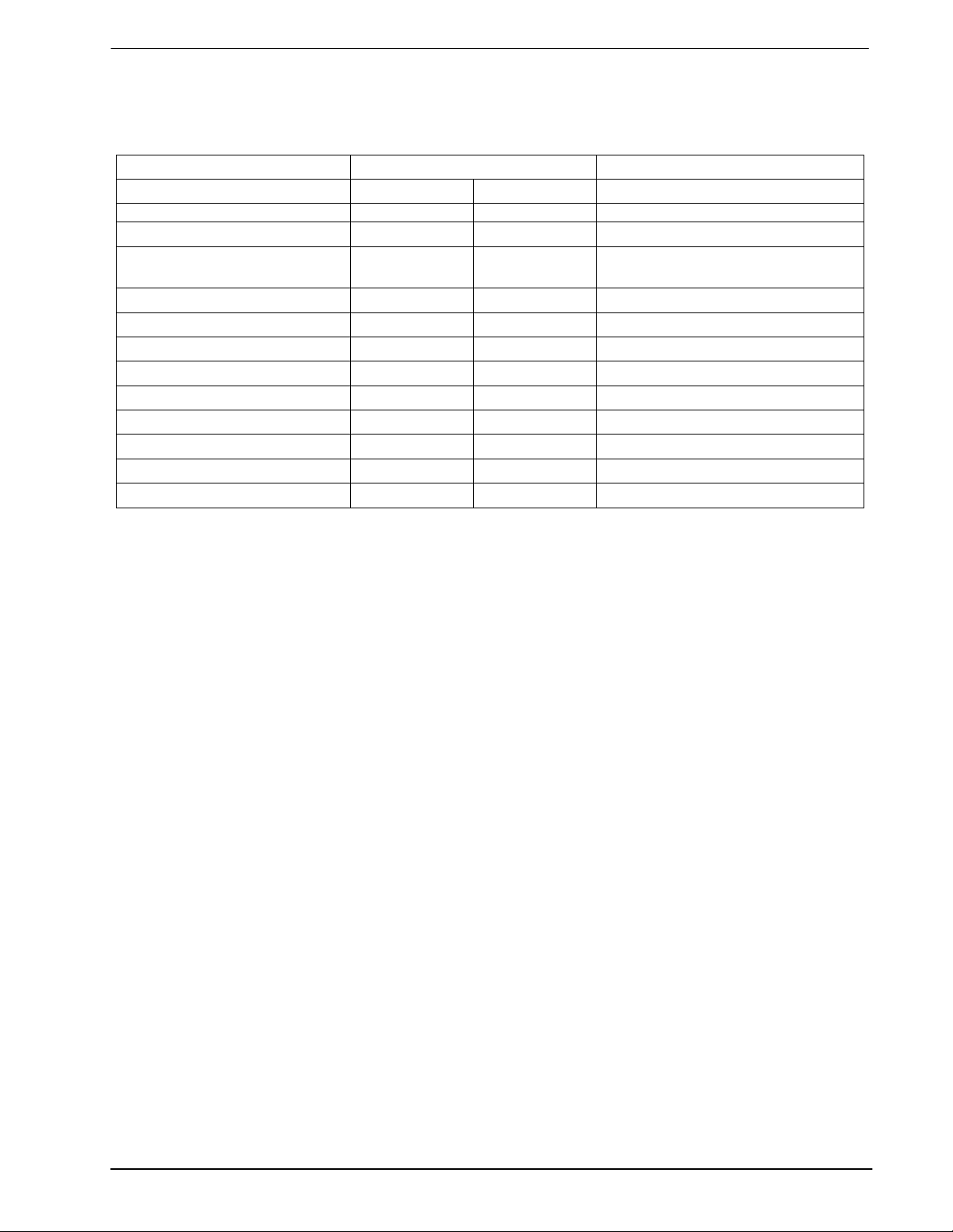
4.1 Controlling Protocol
Control of the functions of the MX802 DVSR Codec is by a group of Address/Commands (A/Cs) and
appended instructions of data to and from the system microcontroller (See Figure 4). The use and content of
these instructions is detailed in the following pages.
Command Assignment Address/Command (A/C) byte Data Bytes
Hex Binary
MSB LSB
General Reset 01 00000001
Write to Control Register 60 01100000 +2 byte instruction to Control
Register
Read Status Register 61 01100001 +1 byte reply from Status Register
Store ‘N’ pages. Start page ‘X’ 62 01100010 +2 bytes command – Immediate
Store ‘N’ pages. Start page ‘X’ 63 01100011 +2 bytes Command – Buffered
Play ‘N’ pages. Start page ‘X’ 64 01100100 +2 bytes Command – Immediate
Play ‘N’ pages. Start page ‘X’ 65 01100101 +2 bytes Command – Buffered
Write Data. Start page ‘P’ 66 01100110 +2 bytes ‘P’ + Write Data
Read Data. Start page ‘P’ 67 01100111 +2 bytes ‘P’ + Read Data
Write Data – continue 68 01101000 +Write Data
Read Data -- Continue 69 01101001 +Read Data
Table 3: C-BUS Address/Commands
4.1.1 Address/Commands
Instruction and data transactions to and from this device consist of an Address/Command (A/C) byte followed
by further instruction/data reply.
Control and configuration is by writing instructions form the microcontroller to the Control Register (60
Reporting of MX802 configurations is by reading the Status Register (61
).
H
).
H
4.1.2 Operation with DRAM
The MX802 can operate with up to 4Mbits of Dynamic Ram (DRAM). When used with DRAM, the MX802
performs four main functions under the control of the commands received over the C-BUS interface from the
microcontroller:
Stores Speech
The MX802 stores speech by digitally encoding the analog input signal and writing the
resulting digital data into the associated DRAM.
Plays Speech
The MX802 plays back stored speech by reading the digital data stored in the DRAM and
decoding it to provide and analog output signal.
Writes Data
Reads Data
The MX802 writes data sent ver the C-BUS from the microcontroller to DRAM.
The MX802 reads data from DRAM, sending it to the microcontroller over the C-BUS.
Data is directed to and from DRAM by the on-chip DRAM Controller.
1998 MX-COM, Inc. www.mxcom.com Tel: 800 638 5577 336 744 5050 Fax: 336 744 5054 Doc. # 20480033.008
4800 Bethania Station Road, Winston-Salem, NC 27105-1201 USA All trademarks and service marks are held by their respective companies.
 Loading...