MX COM Inc MX663DW, MX663P Datasheet

DATA BULLETIN
MX663
Call Progress Decoder
© 1999 MX-COM Inc. www.mxcom.com Tele: 800 638-5577 336 744-5050 Fax: 336 744-5054 Doc. # 20480165.003
4800 Bethania Station Road, Winston-Salem, NC 27105-1201 USA All trademarks and service marks are held by their respective companies.
PRELIMINARY INFORMATION
Features Applications
•
Worldwide Call Progress Tone Decoding:
Single and Dual Tones
Fax and Modem
Answer/Originate Tones
SIT (Special Information Tones)
Fast ‘US Busy’ Tone Detector
•
Adjustable Detection Threshold
•
Voice Detector
•
Low Power 3.3V/5.0V Operation
•
Call Progress Monitoring
Automatic Call Placement
•
Machine Dialing
•
Fax Tone Detection for Line Switching
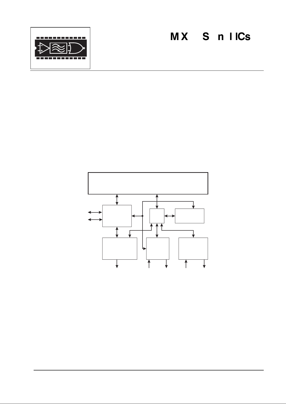
MX663
CALL PROGRESS DECODER
LINE INTERFACE
DTMF
KEYBOARD
AND DISPLAY
DRIVER
AUDIO
PROCESSING
RINGING CURRENT
GENERATOR/
LINE REVERSAL
DETECTOR
DETECTOR AND
µC
CODEC
The MX663 decodes the standard audible tone signals provided by telecom systems worldwide to indicate
Dial, Ringing, Busy, Unobtainable and other stages of a call attempt. It provides the key features needed for
intelligent, full-function, call progress monitoring by applications involving machine dialing or automatic call
placement. The MX663 also incorporates the following features:
•
Single and dual tone decoding for better cross-system Call Progress monitoring.
•
"US Busy" tone detector, saving time needed for "cadence verification" under Busy and Unobtainable
conditions. This incorporates a separate 620Hz detector for improved response.
•
A detector to indicate speech and non-call progress signals; this reduces voice falsing of call progress
tones and adds Voice-Answer detection as a "connected" prompt.
•
A fax and modem tone decoder.
•
A separate, adjustable threshold, signal-level detector which reduces noise falsing.
The MX663 uses digital signal processing techniques to provide these advantages. It is a low cost, low power
product with superior performance. The MX663 may be used with a 3.0 to 5.5 volt supply and is available in
the following packages: 16-pin SOIC (MX663DW) or 16-pin PDIP (MX663P).

Call Progress Decoder 2 MX663 Preliminary Information
© 1999 MX-COM Inc. www.mxcom.com Tele: 800 638-5577 336 744-5050 Fax: 336 744-5054 Doc. # 20480165.003
4800 Bethania Station Road, Winston-Salem, NC 27105-1201 USA All trademarks and service marks are held by their respective companies.
CONTENTS
Section Page
1. Block Diagram................................................................................................................3
2. Signal List.......................................................................................................................4
3. External Components....................................................................................................5
4. General Description.......................................................................................................6
4.1 Overall Function Description ............................................................................................... 6
4.2 Glossary .............................................................................................................................. 6
4.3 Block Diagram Description (Reference Figure 1)................................................................ 6
4.3.1 SIGIN......................................................................................................................................6
4.3.2 Call Progress Detector: Signal Analyzer ................................................................................7
4.3.3 620Hz Detector ......................................................................................................................7
4.3.4 Control and Output Logic ......................................................................................................7
4.3.5 Level Detector and OPAMP ...................................................................................................7
4.3.6 Xtal/Clock Oscillator ...............................................................................................................7
4.3.7 Decode Output Truth Table....................................................................................................8
5. Application .....................................................................................................................9
5.1 General................................................................................................................................ 9
5.2 Signal Category Reference ................................................................................................. 9
5.3 Typical Response.............................................................................................................. 10
6. Performance Specification..........................................................................................11
6.1 Electrical Performance ...................................................................................................... 11
6.1.1 Absolute Maximum Ratings.................................................................................................. 11
6.1.2 Operating Limits...................................................................................................................11
6.1.3 Operating Characteristics.....................................................................................................12
6.2 Timing................................................................................................................................ 13
6.3 Packaging.......................................................................................................................... 16
MX COM, Inc. reserves the right to change specifications at any time and without notice.

Call Progress Decoder 3 MX663 Preliminary Information
© 1999 MX-COM Inc. www.mxcom.com Tele: 800 638-5577 336 744-5050 Fax: 336 744-5054 Doc. # 20480165.003
4800 Bethania Station Road, Winston-Salem, NC 27105-1201 USA All trademarks and service marks are held by their respective companies.
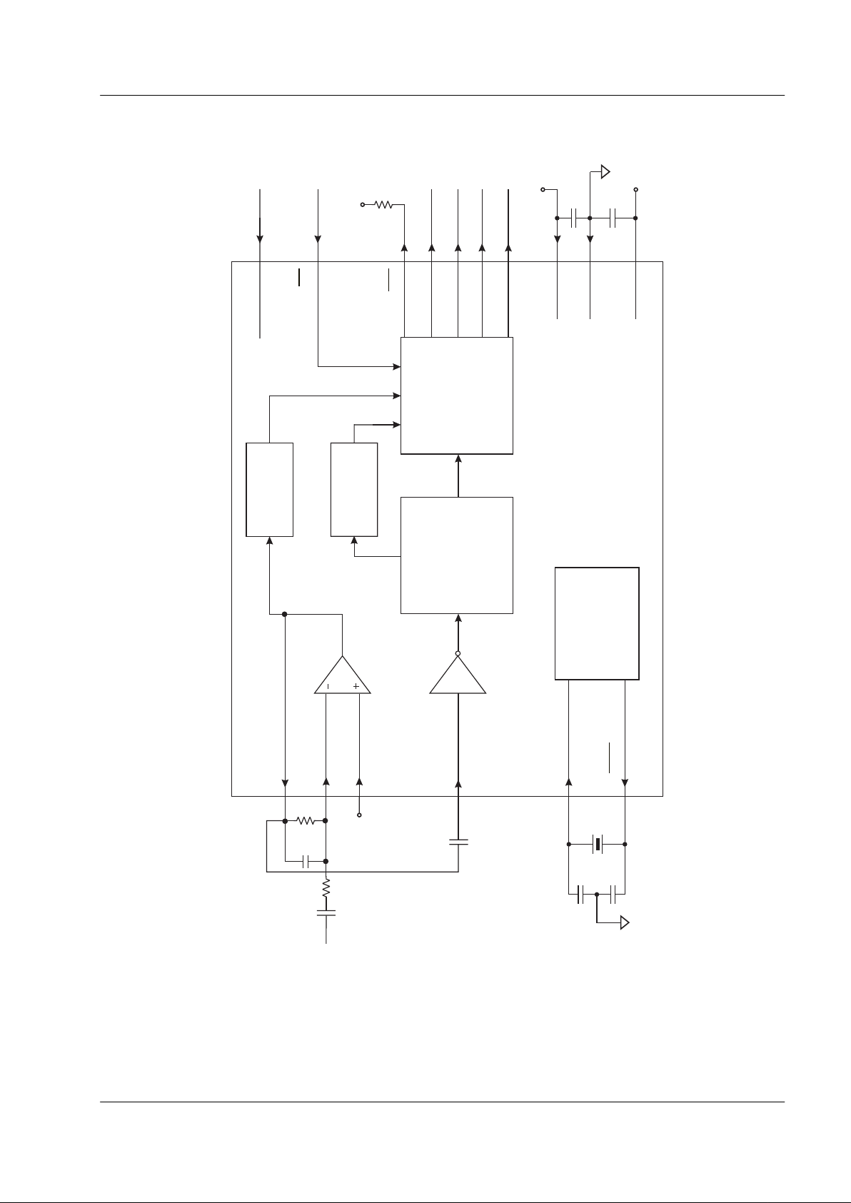
1. Block Diagram
V
BIAS
V
DD
LEVEL
DETECTOR
XTAL/CLOCK
XTAL
C1
C5
C2
X1
R2
R3
R1
CLOCK
OSCILLA TOR
AND
DIVIDERS
OPAMP
SIGIN
AMPOUT
IN-
IN+
ENABLE
C3
C4
CS
IRQ
D0
D2
D1
D3
620Hz
DETECTOR
SIGNAL
ANALYZER
CONTROL
AND
OUTPUT
LOGIC
MX663
SIGNAL
(Components shown for
unbalanced input)
V
SS
V
DD
V
BIAS
V
BIAS
V
DD
C7
C6
Figure 1: Block Diagram

Call Progress Decoder 4 MX663 Preliminary Information
© 1999 MX-COM Inc. www.mxcom.com Tele: 800 638-5577 336 744-5050 Fax: 336 744-5054 Doc. # 20480165.003
4800 Bethania Station Road, Winston-Salem, NC 27105-1201 USA All trademarks and service marks are held by their respective companies.
2. Signal List
Pin No. Signal Type Description
1
XTAL
output Inverted output of the on-chip oscillator.
2 XTAL/CLOCK input Input to the on-chip oscillator, for external Xtal circuit or clock.
3
4
5
6
D3
D2
D1
D0
output D3, D2, D1 and D0 is a 4-bit parallel data word output to the µC. The
transmission of data is under the control of the
CS
input. These 3-
state outputs are held at high impedance when
CS
is at "1". See
Figure 8
If
CS
is permanently at "0", D3, D2, D1 and D0 are permanently active.
See Figure 4 and Figure 7.
7
CS
input The chip select pin activates the Data Bus “D0: 3” when held low. A
µ
C can provide this input to allow the MX663 to reside on a shared
Data Bus. Data transfer sequences are initiated, completed or aborted
by the
CS
signal. See Figure 8
8
IRQ
output This output indicates an interrupt condition to the µC by going to a logic
"0". This is a "wire-ORable" output, enabling the connection of up to 8
peripherals to 1 interrupt port on the µC. This pin has a low impedance
pulldown to logic "0" when active and a high-impedance when inactive.
An external pullup resistor is required.
If
CS
is permanently at "0", the interrupt condition is a logic "0" pulse.
See Figure 4 and Figure 7.
9 ENABLE input A low level input selects the powersave mode, all circuits are reset and
disabled. D0 - D3 outputs become high impedance. A high level input
enables all circuits.
10 V
SS
Power Negative supply (ground).
11 SIGIN input Signal input. The signal to this pin should be ac coupled. The dc bias
of this pin is set internally.
12 V
BIAS
output Internally generated bias voltage, held at VDD/2 when the device is not
in powersave mode, it should be bypassed to V
SS
by a capacitor
mounted close to the device pins. In powersave mode this pin is pulled
towards V
SS
.
13 IN+ input Non-inverting input to the on-chip amplifier.
14 IN- input Inverting input to the on-chip amplifier.
15 AMPOUT output Output of the on-chip amplifier, this is internally connected to the input
of the Level Detector.
16 V
DD
Power The positive supply rail. Levels and voltages are dependent upon this
supply. This pin should be bypassed to V
SS
by a capacitor.
Table 1: Signal List

Call Progress Decoder 5 MX663 Preliminary Information
© 1999 MX-COM Inc. www.mxcom.com Tele: 800 638-5577 336 744-5050 Fax: 336 744-5054 Doc. # 20480165.003
4800 Bethania Station Road, Winston-Salem, NC 27105-1201 USA All trademarks and service marks are held by their respective companies.
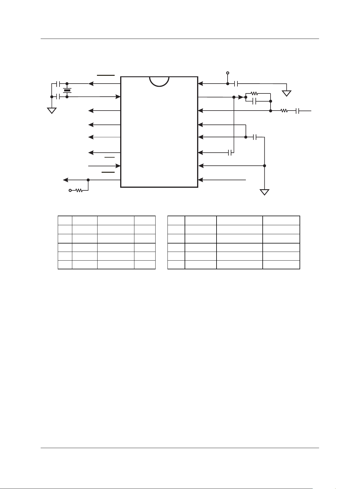
3. External Components
16
15
14
13
12
11
10
9
1
2
3
4
5
6
7
8
V
DD
AMPOUT
IN-
IN+
V
BIAS
SIGIN
ENABLE
R1
R2
C6
C3
C4
C5
C7
V
DD
V
SS
MX663
XTAL
XTAL
IRQ
CS
D3
D1
D2
D0
X1
R3
C1
C2
V
DD
Figure 2: Recommended External Components
R1 Note 3 100k
: ±10% C4 Note 3 0.1µF ±20%
R2 Note 3 510k: ±10% C5 Note 3 100pF ±20%
R3 20k: ±10% C6 1.0µF ±20%
C1 33pF ±20% C7 1µF ±20%
C2 33pF ±20%
C3 0.1µF ±20% X1 Note 1, 2 3.579545MHz ±100ppm
Table 2: Recommended External Components
Notes
1. A standard Color Burst Crystal Frequency is recommended.
2. For best results, a crystal oscillator design should drive the clock inverter input with signal levels of at
least 40% of V
DD
, peak to peak. Tuning fork crystals generally cannot meet this requirement. To
obtain crystal oscillator design assistance, consult your crystal manufacturer.
3. Reference section 4.3.5.
 Loading...