MX COM Inc MX651DW, MX651P Datasheet

DATA BULLETIN
MX651
© 1997 MX
•COM Inc. www.mxcom.com Tele: 800 638-5577 910 744-5050 Fax: 910 744-5054 Doc. # 20480137.003
4800 Bethania Station Road, Winston-Salem, NC 27105-1201 USA
All trademarks and service marks are held by their respective companies.
Telephone
Subscriber Pulse Metering &
Anti Fraud Tone Processor
PRELIMINARY INFORMATION
Features Applications
•
Rapid 18kHz tone encoder-decoder can
transfer NRZ data
Tx up to 166bps
Rx up to 62bps
•
12kHz Subscriber Pulse Metering
Detector
•
Meets European 12kHz SPM Frequency
Specifications
•
Payphone Applications
•
Card Operated Telephone Installations
•
Component Adjustable Input Sensitivity
•
Low Power 3.3V/5.0V Operation
Clock Oscillator
and Dividers
Sample
& Hold
Sample
& Hold
Filtering and
Frequency Detection
12kHz Channel
Digital
Amplifier
Modulator
Band Pass
Filter
V
BIAS
XTAL
XTAL
EXT
CLKIN
NRZ
DAT A
TXOUT
RX/TX
AMPOUT
IN
IN
DETECT
12kHz
DETECT
18kHz
V
SS
V
DD
Filtering and
Frequency Detection
18kHz Channel
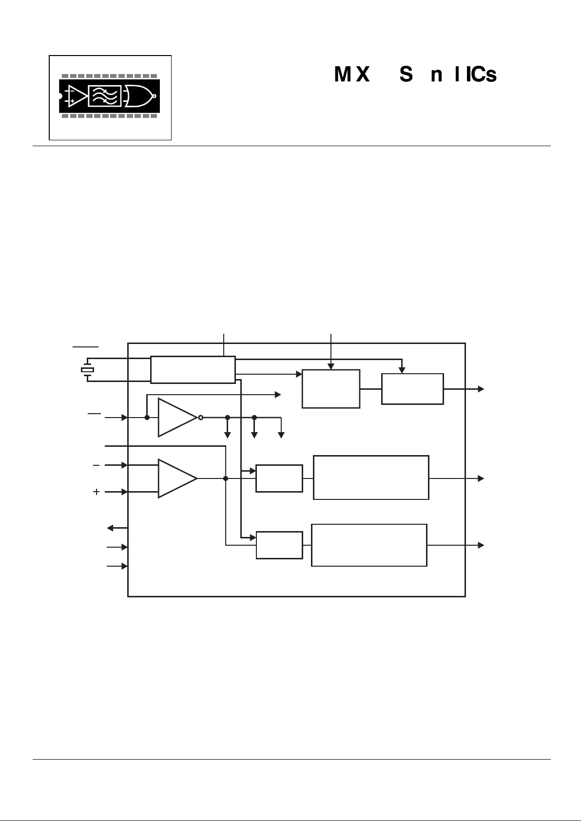
The MX651 is a low power integrated circuit which combines 12kHz Subscriber Pulse Metering (SPM) detection with
18kHz tone processing for anti-fraud purposes within a telephone system. Suitable for battery or line powered systems,
the MX651 is protected from crosstalk and false decoding by employing high accuracy switched capacitor filters. By using
simple logic or µProcessor control the MX651 will:
• Decode 12kHz SPM pulses (in the presence of high level voice and 18kHz signaling) and provide a logic output.
• Transmit an NRZ amplitude modulated 18kHz security tone to line.
• Decode an incoming modulated 18kHz security tone (in the presence of high level voice and 12 kHz SPM tones)
and provide a logic output.
The MX651 is available in a 16-pin SOIC (MX651DW) and a 16-pin PDIP (MX651P) package.

Telephone SPM and Anti Fraud Tone Processor 2 MX651 - PRELIMINARY INFORMATION
© 1997 MX•COM Inc. www.mxcom.com Tele: 800 638-5577 910 744-5050 Fax: 910 744-5054 Doc. # 20480137.003
4800 Bethania Station Road, Winston-Salem, NC 27105-1201 USA
All trademarks and service marks are held by their respective companies.
CONTENTS
Section............................................................................................................................................... Page
1. Block Diagram.................................................................................................................................. 3
2. Signal List......................................................................................................................................... 4
3. External Components...................................................................................................................... 5
4. General Description......................................................................................................................... 6
4.1 Overall Function........................................................................................................................................ 6
4.1.1 SPM (12kHz) Detector.......................................................................................................................................6
4.1.2 Security Tone (18kHz) Detector (Rx Mode Only) ..............................................................................................6
4.1.3 Security Tone Transmission (Tx Mode Only).....................................................................................................6
4.2 Description of Blocks (Reference Figure 1) ............................................................................................ 6
4.2.1 Input Amplifier....................................................................................................................................................6
4.2.2 Sample and Hold (12kHz Channel) ...................................................................................................................6
4.2.3 Filtering and Frequency Detection (12kHz Channel).........................................................................................6
4.2.4 Sample and Hold (18kHz Channel) ...................................................................................................................6
4.2.5 Filtering and Frequency Detection (18kHz Channel).........................................................................................6
4.2.6 Clock Oscillator and Dividers.............................................................................................................................7
4.2.7 (Gate ON-OFF) (Tx Only)..................................................................................................................................7
4.2.8 Band Pass Filter (Tx Only).................................................................................................................................7
5. Application ....................................................................................................................................... 7
5.1 Device Sensitivity versus VDD - Input Amplifier Gain................................................................................ 7
5.2 Alias Responses - False Decodes............................................................................................................7
5.2.1 12kHz Channel ..................................................................................................................................................7
5.2.2 18kHz Channel ..................................................................................................................................................8
6. Performance Specifications............................................................................................................ 8
6.1 Electrical Performance..............................................................................................................................8
6.2 System Timing ......................................................................................................................................... 11
6.2.1 Timing Diagrams ...............................................................................................................................................11
6.3 Packaging ................................................................................................................................................ 12
MX•COM, Inc. reserves the right to change specifications at any time and without notice.

Telephone SPM and Anti Fraud Tone Processor 3 MX651 - PRELIMINARY INFORMATION
© 1997 MX•COM Inc. www.mxcom.com Tele: 800 638-5577 910 744-5050 Fax: 910 744-5054 Doc. # 20480137.003
4800 Bethania Station Road, Winston-Salem, NC 27105-1201 USA
All trademarks and service marks are held by their respective companies.
1. Block Diagram
OSCILLATOR
CLOCK
DIVIDERS
71.591kHz
357.955kHz
17.898kHz
17.898kHz
Modulated on/off
LEVEL
DETECTOR
ZERO
CROSSING
DETECTOR
SAMPLE
AND HOLD
HIGH PASS
FILTER 2
fc = 16kHz
71.591kHz
FREQUENCY
MEASUREMENT
Enable
FREQUENCY
MEASUREMENT
Enable
BAND PASS
FILTER
fc = 18kHz
Gate
357.955kHz
V
DD
V
SS
V
SS
RX/TX
POSIN
NEGIN
AMPOUT
NRZ DATA
3.579545MHz Xtal
CLKIN
XT AL XT AL
Powersave 18kHz Channel
PowersaveTx Circuitry
18kHz Channel
12kHz Channel
17.898kHz
SAMPLE
AND HOLD
HIGH PASS
FILTER 1
fc = 5kHz
LEVEL
DETECTOR
ZERO
CROSSING
DETECTOR
17.898kHz
DIGITAL
AMPLITUDE
MODULATOR
V
BIAS
TXOUT (18kHz ASK Signal)
DETECT 18kHz
V
DD
R1
R3
R5
R4
C4
C3
C1
C2
C5
R2
V
SS
DETECT 12kHz
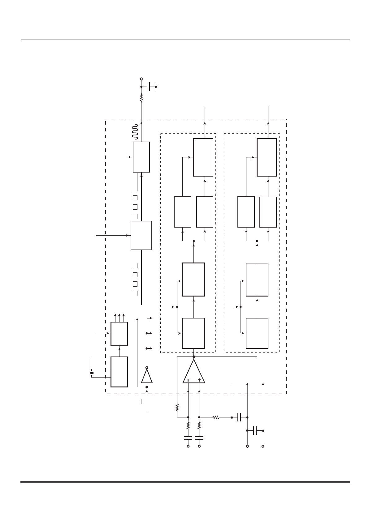
Figure 1: Block Diagram

Telephone SPM and Anti Fraud Tone Processor 4 MX651 - PRELIMINARY INFORMATION
© 1997 MX•COM Inc. www.mxcom.com Tele: 800 638-5577 910 744-5050 Fax: 910 744-5054 Doc. # 20480137.003
4800 Bethania Station Road, Winston-Salem, NC 27105-1201 USA
All trademarks and service marks are held by their respective companies.
2. Signal List
Pin No. Signal Type Description
1 XTAL input Input to the on-chip oscillator inverter.
2
XTAL
output Inverted output of the on-chip oscillator.
4 CLKIN input A logic input which may be used when an external clock signal is available in
place of a crystal. The external 3.579545MHz signal is applied to this pin and
XTAL is tied to V
DD
. When not used, this pin should be tied to VDD.
5
RX/ TX
input A logic input which controls the operating mode of the device. In Rx, the
device detects the presence of 12kHz and 18kHz tones. In Tx, the18kHz
detect function is disabled and 18kHz is transmitted from the TXOUT pin
modulated ON -OFF by the NRZ Data pin.
6 NRZ DATA input A logic input used in Tx mode to ASK modulate the TXOUT pin. A logic high
corresponds to no tone and logic low corresponds to 18kHz.
7 TXOUT output The Tx mode output. It is ASK modulated by the NRZ data input pin. It
transmits 18kHz or no tone depending upon the state of the NRZ data input
pin. This pin goes to a high impedance state when in Rx mode.
8VSSpower Negative supply.
9V
BIAS
output A bias line for the internal circuitry, held at VDD/2 It also forms the analog
ground for the input differential amplifier. This pin must be bypassed by a
capacitor mounted close to the device pins (see Figure 1).
10 AMPOUT output Output of the input amplifier. External components are used in conjunction
with the amplifier to couple the line signal into the device. Both inputs are
available to allow a differential configuration because a two wire input is
assumed.
11 NEGIN input Inverting input to the input amplifier.
12 POSIN input Non-inverting input to the input amplifier.
13 DETECT 18kHz output Logic output of the 18kHz channel. Logic 0 when a 18kHz tone (within
specified frequency and amplitude limits) has been detected for a minimum
length of time.
14 DETECT 12kHz output Logic output of the 12kHz channel. Logic 0 when a 12kHz tone (within
specified frequency and amplitude limits) has been detected for a minimum
length of time.
16 V
DD
power Positive Supply. Levels and voltages are dependent upon this supply. This
pin should be bypassed to V
SS
by a capacitor (see Figure 1).
3, 15 N/C No internal connection: leave open circuit.
 Loading...