

MX COM Inc MX643DW, MX643P Datasheet
DATA BULLETIN
© 1996 MX•COM, INC. Tele: 800 638 5577, 910 744 5050, Fax: 910 744 5054
Document #20480148.001 May 1996
Preliminary Information
• • International Special Information Tone Identification
• • Worldwide Tone Compatibility • • - 40°°C to 85°°C Operating Temp
• • Single and Dual Tone Detected • • Low Supply Current (0.3mA/0.5mA)
• • U.S. Busy-Detect Output • • Low Supply Voltage (3.3V/5.0V)
• • Voice-Detect Output • • Standard 3.58MHz Clock Input
• • Wide Dynamic Range > 40dBm • • Standard 8-pin DIP Package
DETECT2
DETECT3
DETECT1
SLICER
SIGIN
ENABLE
XTAL
SIGNAL
ANALYZER
CONTROL
LOGIC
CLOCK
V
SS
V
DD
CLOCK /
XTAL
AVAILABLE
PACKAGES
MX643P
8-pin PDIP
MX643DW
16-pin SOIC
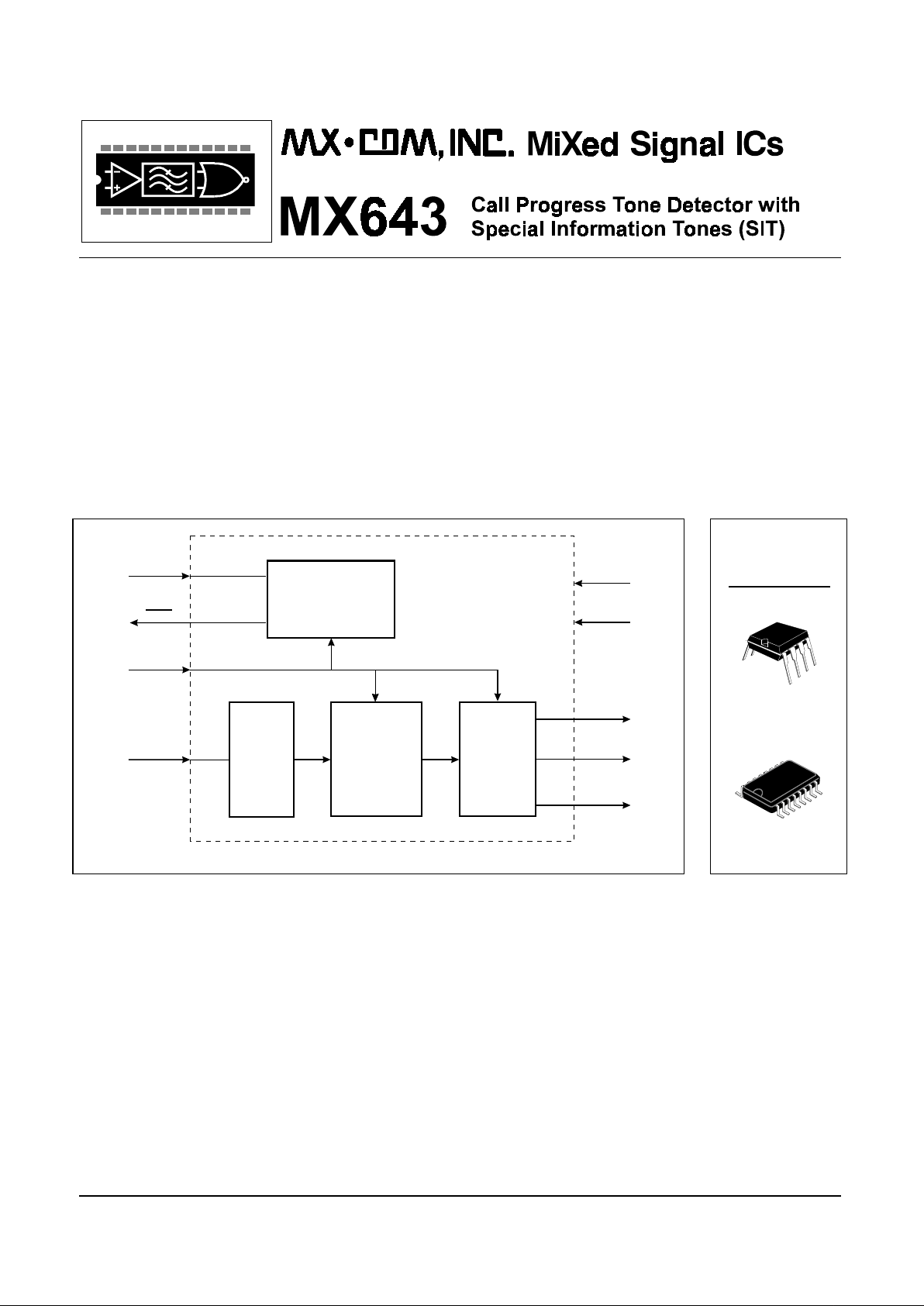
The MX643 is a low power, low cost device that uses signal processing techniques to detect audible tone signals
such as; Dial, Ring, Busy, Unobtainable, and other conditions found when placing a call throughout the world’s
telecom systems. The detection of these Call Progress stages is essential to the proper operation and application
of automatic calling products.
The MX643 offers identification of International Special Information Tones (SIT), reducing the time needed for
cadence verification under Obtainable conditions. In addition to the SIT feature, single and dual tone decoding
are added for better cross-system Call Progress monitoring. The MX643 offers these features in addition to the
same performance levels and features of the MX633 Call Progress Tone Detector such as; detection and
identification of U.S. Busy tones, thereby reducing the need to measure the tone cadence to identify U.S. Busy.
The decoding and indicating of speech, or other Non-Call Progress signals, thus reducing voice-falsing of Call
Progress tones and adding Voice-Answer as a connect prompt.
Available in the industry standard 8-pin DIP, the MX643 is also available in a 16-pin SOIC making it pin
compatible with the MX633DW (16-pin SOIC).

Call Progress Tone Detector MX643 - Preliminary Information
© 1996 MX•COM, INC. Tele: 800 638 5577, 910 744 5050, Fax: 910 744 5054 Doc. #20480148.001
2
CONTENTS
Section Page
1. Block Diagram...............................................................................................................3
2. Signal List......................................................................................................................4
3. External Components...................................................................................................5
4. General Description......................................................................................................5
4.1 Glossary ............................................................................................................................ 5
4.2 Overall Function Description ............................................................................................. 6
5. Block Diagram Description..........................................................................................6
5.1 Decode Output Truth Table............................................................................................... 7
6. Performance Specification ..........................................................................................7
6.1 Electrical Performance...................................................................................................... 7
6.2 Packaging......................................................................................................................... 11
MX•COM, Inc. reserves the right to change specifications at any time and without notice.
Call Progress Tone Detector MX643 - Preliminary Information
© 1996 MX•COM, INC. Tele: 800 638 5577, 910 744 5050, Fax: 910 744 5054 Doc. #20480148.001
3
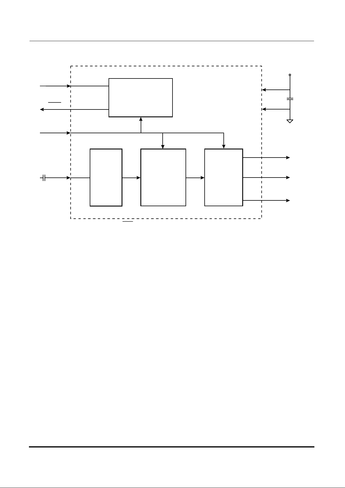
1. Block Diagram
DETECT2
DETECT3
DETECT1
SLICER
SIGIN
ENABLE
XTAL
SIGNAL
ANALYZER
CONTROL
LOGIC
CLOCK
V
SS
V
DD
V
DD
C1
C2
CLOCK /
XTAL
Note: used for 16-pin SOIC (MX643DW) only.XTAL
Figure 1: Block Diagram
Call Progress Tone Detector MX643 - Preliminary Information
© 1996 MX•COM, INC. Tele: 800 638 5577, 910 744 5050, Fax: 910 744 5054 Doc. #20480148.001
4
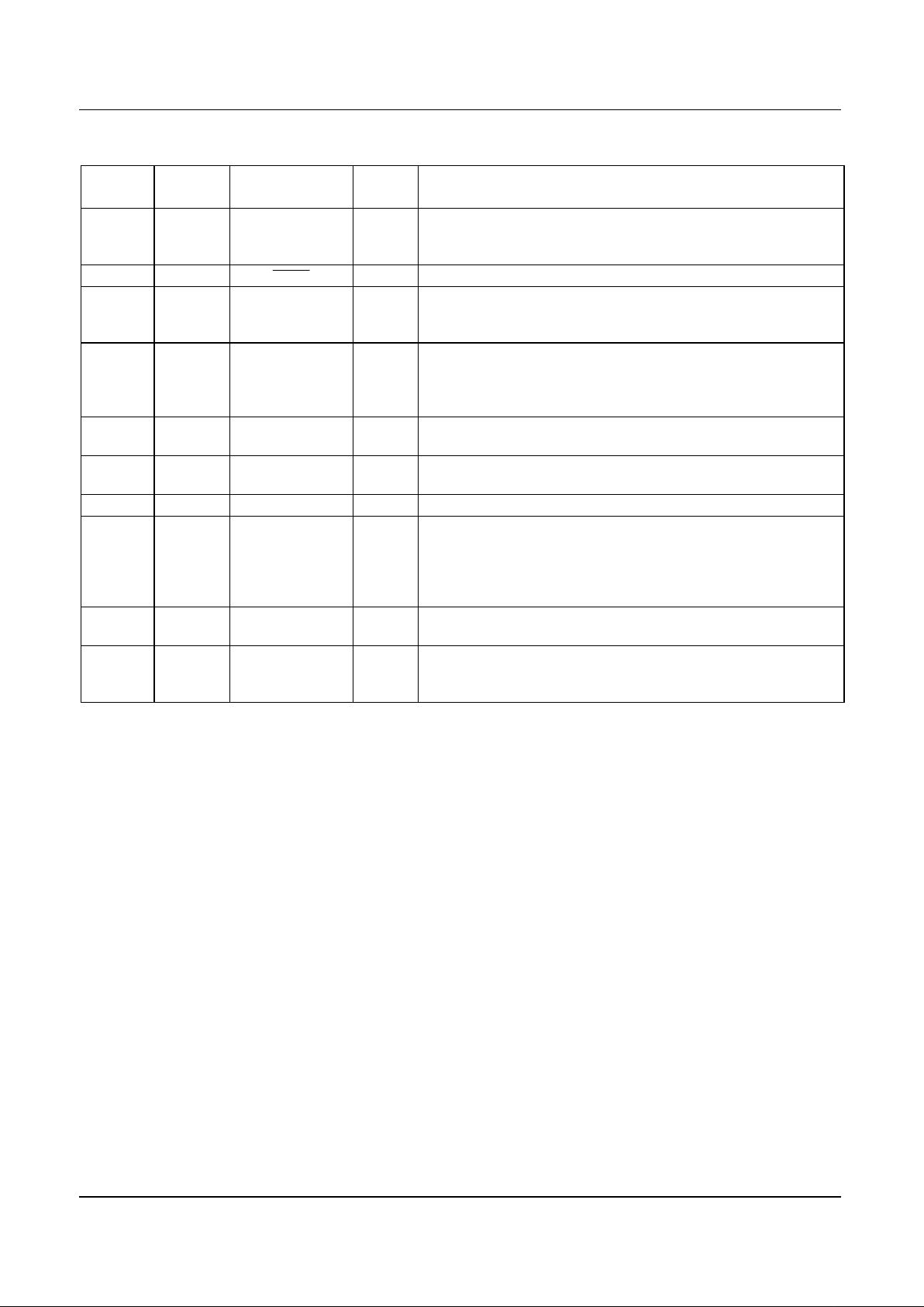
2. Signal List
P-Pin
No.
DW-Pin
No.
Signal Type Description
1 2 CLOCK / XTAL input For the MX643P this is the external clock input to the clock
divider circuit. For the MX643DW this can be either an
external clock input or an external crystal input.
-3
XTAL
output Output of the on-chip oscillator. Not available on 8-pin DIP..
2 4 DETECT3 output When a single tone is within the range of the Call Progress
Band, Non Call Progress Band, or a Special Information
Tone, is detected, this output goes to a logic 1.
3 5 ENABLE input A logic 1 applied to this input enables the decoder and
detection outputs. A logic 0 applied to this input disables the
decoder and forces DETECT1, DETECT2 and DETECT3 to a
logic 0.
4 7 DETECT1 output When a call progress signal is detected, this output goes to a
logic 1.
5 10 SIGIN input Signal input. Signals to this pin should be ac coupled. The dc
bias of this pin is set internally.
612 VSSpower Negative supply. (ground).
7 13 DETECT2 output This output is used in conjunction with DETECT1. When
DETECT1 is at a logic 1, this output goes to a logic 1 if a Call
Progress High Band signal is detected. When DETECT1 is
at a logic 0, this output goes to a logic 1 if a Non Call
Progress signal is detected.
815 VDDpower Positive supply. This pin should be decoupled to VSS by a
capacitor.
1, 6, 8,
9, 11,
14, 16
N/C Internal connection. Do not make a connection to these pins.
 Loading...