DATA BULLETIN
MX641
Dual SPM Detector
Features Applications
x Two (12kHz / 16kHz) SPM Detectors on a
Single Chip
x Detects 12 or 16kHz SPM Frequencies
x ‘Controlled’ (PC) & ‘Fixed’ Signal Sensitivity
Modes
x Selectable Tone Follower or Packet Mode
Outputs
x High Speech-Band Rejection Properties
x ‘Output Enable’ Multiplexing Facility
XTAL/CLOCK
XTAL
Ch1AMPOUT
Ch1 AMP IN (-)
Ch1 AMP IN (+)
PRESET LEVEL
CHIP SELECT
SERIAL
DATA
SERIAL
CLOCK
SYSTEM SELECT
Ch2 AM PIN (-)
Ch2 AMP IN (+)
Ch2AMPOUT
+
Ch 1
INPUT
AMPLIFIER
SERIAL
INPUT
LOGIC
Ch 2
INPUT
AMPLIFIER
+
XTAL/CLOCK
GENERATOR
Ch 1
BANDPASS
FILTER
GAIN
ADJUST
LEVEL/
SYSTEM
SETTING
GAIN
ADJUST
Ch 2
BANDPASS
FILTER
COMPARATOR
THRESHOLD
COMPARATOR
THRESHOLD
CLOCK OUT CLOCK IN
BUFFER
Ch 1
COMPARATOR
+
INTERNAL
12kHz/16kHz
SYSTEM
INTERNAL
+
-
Ch 2
COMPARATOR
x Call Charge Applications on PABX Line
Cards
x Remote Telephone Applications
CLOCK
DIVIDERS
12kHz/16kHz
PULSE
GENERATOR
AND
DIVIDER
CHANNEL 1
CHANNEL 2
PULSE
GENERATOR
AND
DIVIDER
SYSTEM
PULSE
MEASUREMENT
LOGIC
PULSE
MEASUREMENT
LOGIC
TONE FOLLOWER
PULSE
LENGTH
LOGIC
PULSE
LENGTH
LOGIC
TONE FOLLOWER
PRELIMINARY INFORMATION
V
DD
V
OUTPUT
SELECT
CIRCUITS
OUTPUT
SELECT
CIRCUITS
V
Ch 1
OUTPUT
OUTPUT
ENABLE
OUTPUT
SELECT
Ch 2
OUTPUT
BIAS
SS
MODE
MODE
INTERNAL
CLOCKS
PACKET
MODE
12kHz/16kHz
SYSTEM
PACKET
MODE
The MX641 is a low-power, system-selectable Dual Subscriber Pulse Metering (SPM) Detector designed to indicate the
presence, on a telephone line, of either 12kHz or 16kHz telephone call-charge frequencies. It is designed for PBX and
PABX line-card and remote telephone installations. Under PProcessor control via a common serial interface, each
channel of the MX641 will detect call-charge pulses from a telephone line and provide a digital output for recording, billing
or security purposes. A common set of external components and a stable 3.579545MHz Xtal/clock input ensures that the
MX641 adheres accurately to most national “Must and Must-Not” decode band-edges and threshold levels. For nonPProcessor systems a preset sensitivity/system input allows external channel level and system setting
The digital output is pin-selectable to one of three modes:
(1) Tone Follower mode: logic level for the period of a correct decode.
(2) Packet mode: respond/de-respond after a cumulative period of tone or notone in a fixed (intrinsic hardwired period
that is not user controlled) period.
(3) High-impedance output: for device multiplexing.
The MX641 requires a 5V supply and is available in the following packages: 24-pin SOIC (MX641DW) and 24-pin PDIP
(MX641P).
© 1998 MX
4800 Bethania Station Road, Winston-Salem, NC 27105-1201 USA All trademarks and service marks are held by their respective companies.
xCOM Inc. www.mxcom.com Tele: 800 638-5577 910 744-5050 Fax: 910 744-5054 Doc. # 20480115.003

Dual SPM Detector 2 MX641 PRELIMINARY INFORMATION
CONTENTS
Section Page
1. Block Diagram.................................................................................................................................. 3
2. Signal List......................................................................................................................................... 4
3. External Components...................................................................................................................... 6
4. General Description......................................................................................................................... 7
4.1 Xtal/Clock Distribution............................................................................................................................... 7
4.2 Channel Outputs....................................................................................................................................... 7
4.3 Sensitivity Setting...................................................................................................................................... 8
4.3.1 Controlled Sensitivity Setting.............................................................................................................................8
4.3.2 Fixed Sensitivity Setting....................................................................................................................................11
5. Applications .................................................................................................................................... 12
5.1.1 Input Configurations..........................................................................................................................................12
5.1.2 Protection Against High Voltages .....................................................................................................................12
5.1.3 Aliasing .............................................................................................................................................................12
6. Performance Specification............................................................................................................. 13
6.1 Electrical Specifications ........................................................................................................................... 13
6.1.1 Absolute Maximum Ratings..............................................................................................................................13
6.1.2 Operating Limits................................................................................................................................................13
6.1.3 Operating Characteristics .................................................................................................................................13
6.2 Timing ...................................................................................................................................................... 15
6.3 Packages ................................................................................................................................................. 16
MXxCOM, Inc. reserves the right to change specifications at any time and without notice.
© 1998 MXxCOM Inc. www.mxcom.com Tele: 800 638-5577 910 744-5050 Fax: 910 744-5054 Doc. # 20480115.003
4800 Bethania Station Road, Winston-Salem, NC 27105-1201 USA All trademarks and service marks are held by their respective companies.

Dual SPM Detector 3 MX641 PRELIMINARY INFORMATION
1. Block Diagram
DDVBIASVSS
V
CLOCKS
INTERNAL
CLOCK
DIVIDERS
TONE FOLLOWER
SYSTEM
12kHz/16kHz
Ch 1
MODE
OUTPUT
OUTPUT
PULSE
PULSE
MEASUREMENT
PULSE
GENERATOR
SELECT
CIRCUITS
LOGIC
LENGTH
LOGIC
AND
DIVIDER
MODE
PACKET
CHANNEL 1
ENABLE
OUTPUT
SYSTEM
12kHz/16kHz
SELECT
OUTPUT
CHANNEL 2
MODE
PACKET
SELECT
OUTPUT
CIRCUITS
LOGIC
PULSE
LENGTH
LOGIC
PULSE
MEASUREMENT
AND
PULSE
DIVIDER
GENERATOR
Ch 2
OUTPUT
TONE FOLLOWER
MODE
CLOCK OUT CLOCK IN
XTAL/CLOCK
XTAL/CLOCK
BUFFER
GENERATOR
XTAL
SYSTEM
12kHz/16kHz
-
Ch 1
COMPARATOR
Ch1AMPOUT
+
INTERNAL
THRESHOLD
COMPARATOR
LEVEL/
SERIAL
DATA
SERIAL
SYSTEM
SETTING
INPUT
LOGIC
Ch 1
FILTER
BANDPASS
-
Ch1 AMP IN (-)
GAIN
ADJUST
Ch 1
INPUT
+
AMPLIFIER
PRESET LEVEL
Ch1 AMP IN (+)
CHIP SELECT
SERIAL
CLOCK
INTERNAL
THRESHOLD
COMPARATOR
GAIN
Ch 2
SYSTEM SELECT
ADJUST
INPUT
AMPLIFIER
-
+
Ch 2
-
Ch2 AMP IN (-)
BANDPASS
+
FILTER
Ch 2
COMPARATOR
Ch2AMPOUT
Ch2 AMP IN (+)
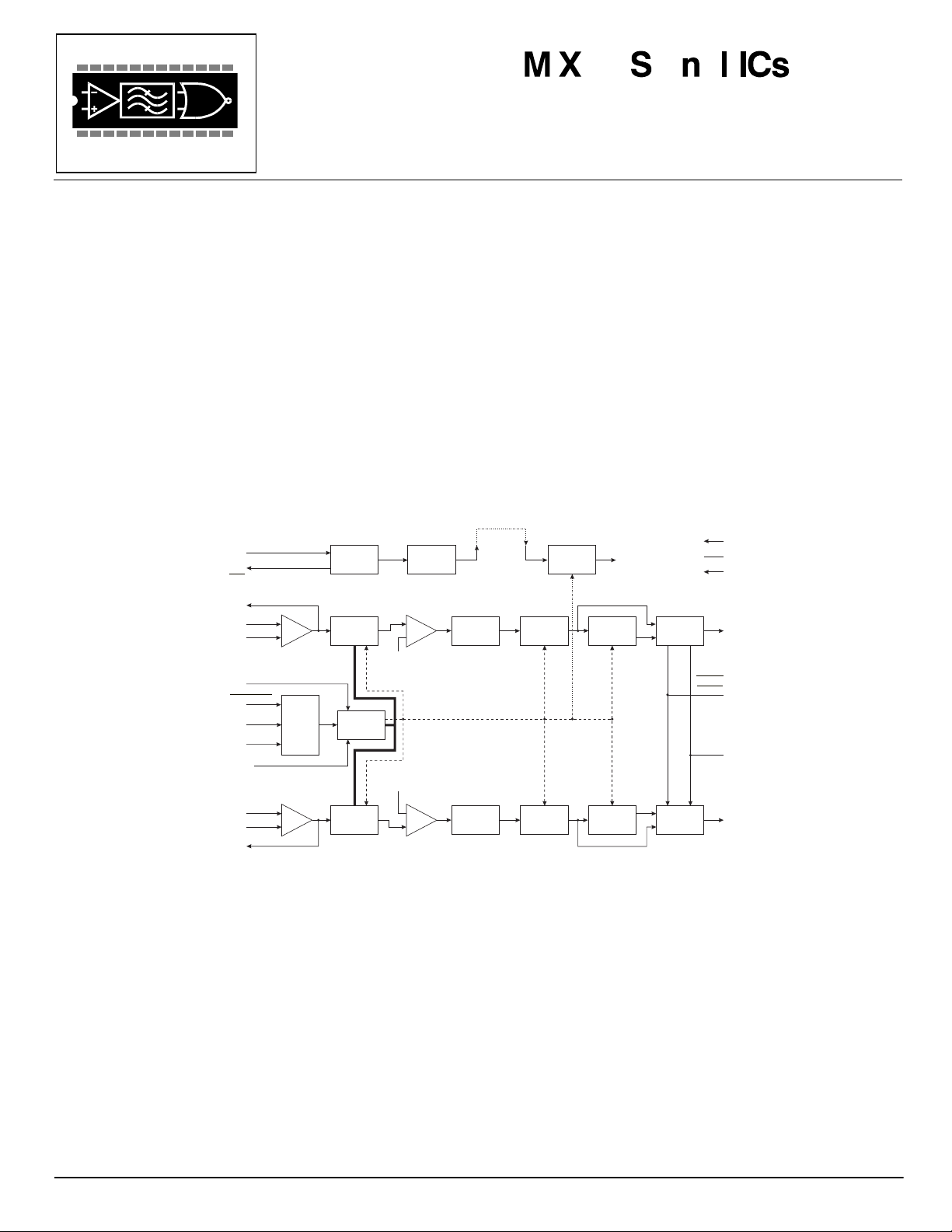
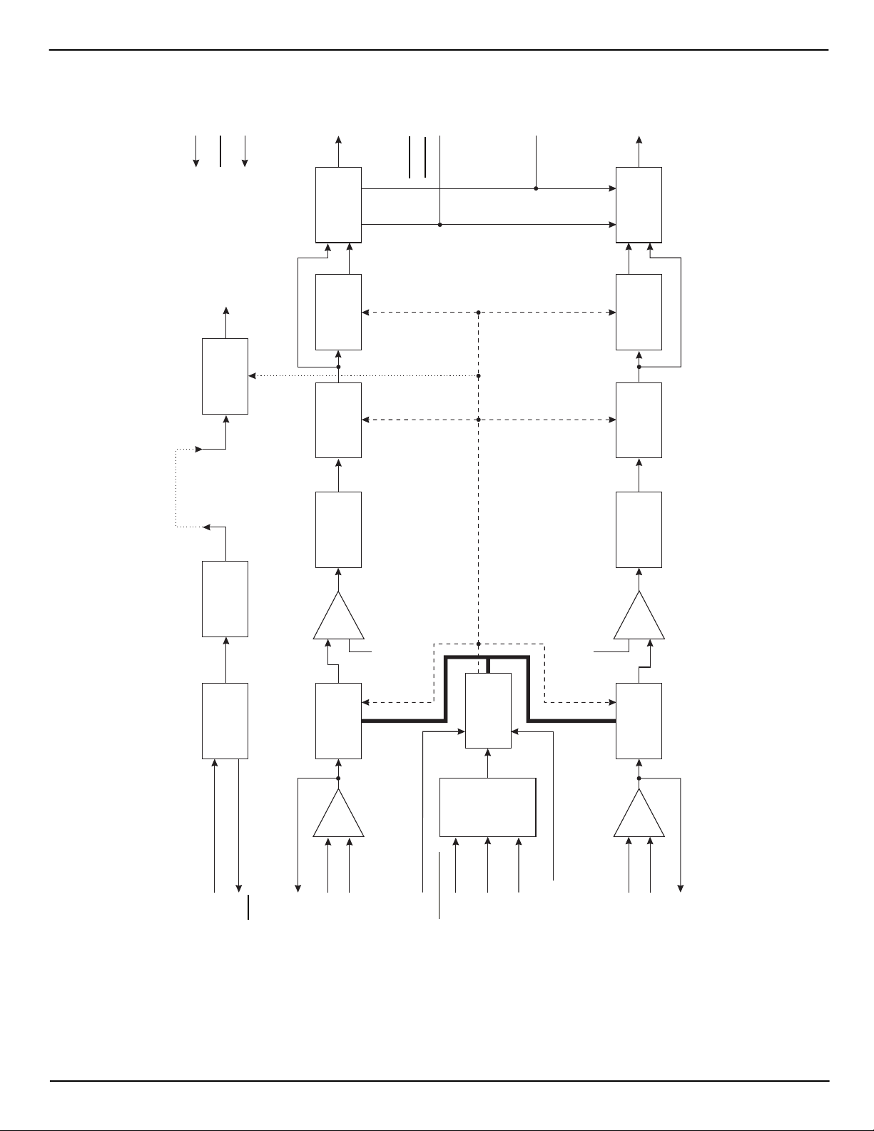
Figure 1: Block Diagram
© 1998 MXxCOM Inc. www.mxcom.com Tele: 800 638-5577 910 744-5050 Fax: 910 744-5054 Doc. # 20480115.003
4800 Bethania Station Road, Winston-Salem, NC 27105-1201 USA All trademarks and service marks are held by their respective companies.

Dual SPM Detector 4 MX641 PRELIMINARY INFORMATION
2. Signal List
Pin No. Name Type Description
1 Xtal/Clock input The input to the on-chip clock oscillator; for use with a 3.579545MHz Xtal in
conjunction with the Xtal output; circuit components are on-chip. When using a
Xtal input, the Clock Out pin should be connected directly to the Clock In pin. If
a clock pulse input is used at the Clock In pin, this (Xtal/Clock) pin must be
connected directly to V
frequency distribution.
2
XTAL
output The output of the on-chip clock oscillator inverter.
3 Clock Out output The buffered output of the on-chip-clock oscillator inverter. If a Xtal input is
used, this output should be connected directly to the Clock In pin. This output
can support up to 3 additional MX641 ICs. See Figure 3 for details of clock
frequency distribution.
4 Clock In input The 3.579545 clock pulse input to the internal clock dividers. If an externally
generated clock pulse input is used, the Xtal/Clock input pin should be
connected to V
5
Output Enable
input For multi-chip output multiplexing; controls the state of both Ch1 and Ch2
DD
.
outputs. When this input is placed high (logic '1') both outputs are set to a high
impedance. When placed low (logic '0') both outputs are enabled.
6 Ch 2 Output output The digital output of the Channel 2 SPM detector when enabled. The format of
the signal at this pin, in common with Ch 1, is selectable to either
'Tone Follower' or 'Packet' mode via the Output Select input.
7 Ch 1 Output output The digital output of the Channel 1 SPM detector when enabled. The format of
the signal at this pin, in common with Ch 2, is selectable to either
'Tone Follower' or 'Packet' mode via the Output Select input.
8V
BIAS
power The output of the on-chip analog bias circuitry. Held internally at VDD/2, this
pin should be decoupled to V
9 Ch 1 Amp Out output The output of the Channel 1 Input Amplifier. See Figure 2 and Figure 8.
10 Ch 1 Amp In (-): input The negative input to the Channel 1 Input Amplifier. See Figure 2 and Figure
8.
11 Ch 1 Amp In (+): input The positive input to the Channel 1 Input Amplifier. See Figure 2 and Figure 8.
12 V
SS
power Negative supply (GND).
13 N/C No internal connection; leave open circuit.
14 Ch 2 Amp In (+): input The positive input to the Channel 2 Input Amplifier. See Figure 2 and Figure 8.
15 Ch 2 Amp In (-): input The negative input to the Channel 2 Input Amplifier. See Figure 2 and Figure
8.
16 Ch 2 Amp Out output The output of the Channel 2 Input Amplifier. See Figure 2 and Figure 8.
17 Output Select input A logic input to set the Channel 1 and Channel 2 output modes. When high
(logic '1'), the outputs are in the Tone Follower mode; when low (logic '0'), the
outputs are in the Packet mode.
18 Preset Level input A logic input to set the sensitivity mode of the MX641. When high (logic '1'),
both channels are in the Fixed Sensitivity mode. The external components
govern the input sensitivity; the System Select input selects 12kHz or 16kHz
operation. When low (logic '0'), both channels are in the Controlled Sensitivity
mode. Device sensitivities and system selection are via the Chip Select/Serial
Data/Serial Clock inputs. This input has an internal pullup resistor on chip
(Fixed Sensitivity Mode).
19
Chip Select
input The Chip Select input for use in data loading when using the MX641 in the
Controlled Sensitivity mode (see Figure 9). The device is selected when this
input is set low (logic '0'). When the MX641 is in the Fixed Sensitivity mode
this input should be connected to either V
(see Figure 2). See Figure 3 for details of clock
DD
(see Figure 2).
SS
or VDD.
SS
© 1998 MXxCOM Inc. www.mxcom.com Tele: 800 638-5577 910 744-5050 Fax: 910 744-5054 Doc. # 20480115.003
4800 Bethania Station Road, Winston-Salem, NC 27105-1201 USA All trademarks and service marks are held by their respective companies.

Dual SPM Detector 5 MX641 PRELIMINARY INFORMATION
Pin No. Name Type Description
20 Serial Clock input The Serial Clock input for use in data loading when using the MX641 in the
Controlled Sensitivity mode (see Figure 9). Data is loaded to the MX641 on
this clock's rising edge. When the MX641 is in the Fixed Sensitivity mode this
input should be connected to either V
or VDD.
SS
21 Serial Data input The Serial Data input for use in data loading when using the MX641 in the
Controlled Sensitivity mode (see Figure 9 and Table 4). When the device is in
the Fixed Sensitivity mode this input should be connected to either V
or VDD.
SS
22 System Select input In the Fixed Sensitivity mode this pin selects the system frequency. High (logic
‘1’) = 12kHz; Low (logic ‘0’) = 16kHz. In the Controlled Sensitivity mode this pin
is inactive and may be left unconnected. This pin has an internal pullup
resistor on chip.
23 N/C No internal connection; leave open circuit.
24 V
DD
power Positive supply rail; a single, stable power supply is required. Critical levels
and voltages within the MX641 are dependent upon this supply. This pin
should be decoupled to V
by a capacitor mounted close to the pin
SS
Table 1: Signal List
© 1998 MXxCOM Inc. www.mxcom.com Tele: 800 638-5577 910 744-5050 Fax: 910 744-5054 Doc. # 20480115.003
4800 Bethania Station Road, Winston-Salem, NC 27105-1201 USA All trademarks and service marks are held by their respective companies.
 Loading...