DATA BULLETIN
MX633
Call Progress Tone Detector
© 1997 MX
•COM Inc. www.mxcom.com Tele: 800 638-5577 910 744-5050 Fax: 910 744-5054 Doc. # 20480135.003
4800 Bethania Station Road, Winston-Salem, NC 27105-1201 USA All trademarks and service marks are held by their respective companies.
PRELIMINARY INFORMATION
Features Applications
•
Worldwide Tone Compatibility
•
Single and Dual Tones Detected
•
U.S. Busy-Detect Output
•
Voice-Detect Output
•
Wide Dynamic Range > 40dBm
•
Low Supply Current (0.3mA/0.5mA)
•
Low Supply Voltage (3.3V/5.0V)
•
Standard 3.58MHz Xtal
•
Automatic Calling Products
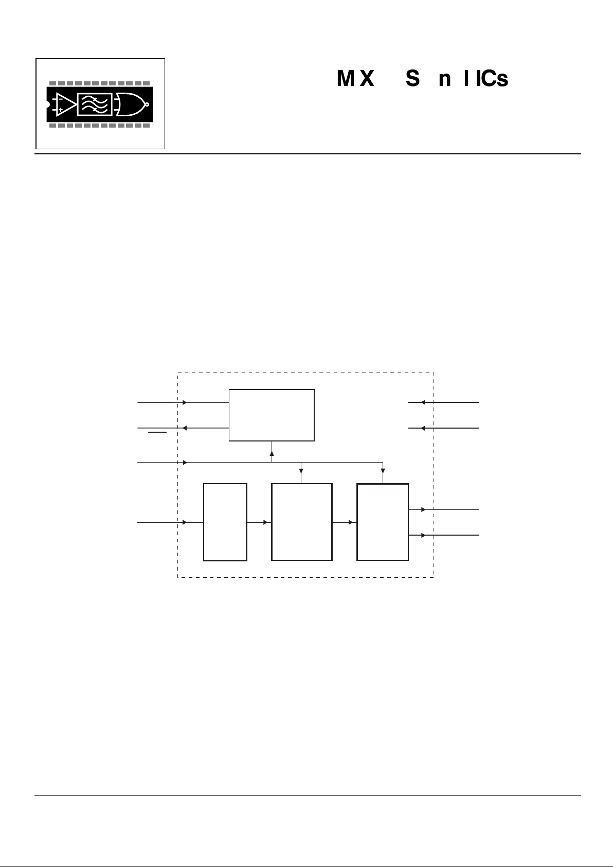
DETECT2
DETECT1
SLICER
SIGIN
XTAL/
CLOCK
SIGNAL
ANALYZER
CONTROL
LOGIC
XTAL/ CLOCK
OSCILLATOR
V
SS
V
DD
XTAL
ENABLE
The MX633 is a low cost, low power device that uses signal processing techniques to detect audible tone signals such as
Dial, Ringing, Busy and other conditions found when placing a call throughout the world’s telecom systems. Detection of
these call progress stages is essential to the proper operation of automatic calling products.
The MX633 adds new features to Call Progress monitoring. It detects and indicates the ‘U.S. Busy’ tones, reducing the
need to measure ‘tone cadence’ to identify ‘U.S. Busy’. It also detects and indicates voice and other signals from Call
Progress tones, reducing voice-falsing and adding voice-answer as a connection prompt.
The MX633 may be used with a 3.0V to a 5.5V supply and is available in the following package styles: 8-pin PDIP
(MX633P) and 16-pin SOIC (MX633DW).

Call Progress Tone Detector 2 MX633 - PRELIMINARY INFORMATION
© 1997 MX•COM Inc. www.mxcom.com Tele: 800 638-5577 910 744-5050 Fax: 910 744-5054 Doc. # 20480135.003
4800 Bethania Station Road, Winston-Salem, NC 27105-1201 USA All trademarks and service marks are held by their respective companies.
CONTENTS
Section...............................................................................................................................................Page
1. Block Diagram.................................................................................................................................. 3
2. Signal List......................................................................................................................................... 4
3. External Components...................................................................................................................... 5
4. General Description......................................................................................................................... 6
4.1 Glossary.................................................................................................................................................... 6
4.2 Overall Function Description..................................................................................................................... 6
4.3 Block Diagram Description (Reference Figure 1)......................................................................................6
4.3.1 Slicer..................................................................................................................................................................6
4.3.2 Signal Analyzer..................................................................................................................................................6
4.3.3 Control Logic......................................................................................................................................................7
4.3.4 Xtal/Clock Oscillator...........................................................................................................................................7
4.4 Decode Output Truth Table.......................................................................................................................7
5. Performance Specification.............................................................................................................. 7
5.1 Electrical Performance.............................................................................................................................. 7
5.1.1 Absolute Maximum Ratings...............................................................................................................................7
5.1.2 Operating Limits.................................................................................................................................................8
5.1.3 Operating Characteristics ..................................................................................................................................8
5.1.4 Timing................................................................................................................................................................9
5.2 Packaging ................................................................................................................................................11
MX•COM, Inc. reserves the right to change specifications at any time and without notice

Call Progress Tone Detector 3 MX633 - PRELIMINARY INFORMATION
© 1997 MX•COM Inc. www.mxcom.com Tele: 800 638-5577 910 744-5050 Fax: 910 744-5054 Doc. # 20480135.003
4800 Bethania Station Road, Winston-Salem, NC 27105-1201 USA All trademarks and service marks are held by their respective companies.
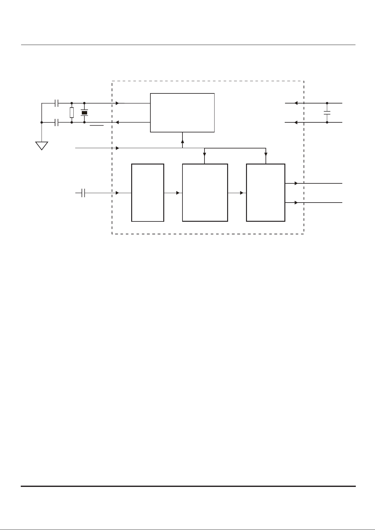
1. Block Diagram
DETECT2
DETECT1
SLICER
SIGIN
XTAL/
CLOCK
SIGNAL
ANALYZER
CONTROL
LOGIC
C1
C4
R1
X1
C2
C3
XTAL / CLOCK
OSCILLA TOR
V
SS
V
DD
XTAL
ENABLE
Figure 1: Block Diagram

Call Progress Tone Detector 4 MX633 - PRELIMINARY INFORMATION
© 1997 MX•COM Inc. www.mxcom.com Tele: 800 638-5577 910 744-5050 Fax: 910 744-5054 Doc. # 20480135.003
4800 Bethania Station Road, Winston-Salem, NC 27105-1201 USA All trademarks and service marks are held by their respective companies.
2. Signal List
Package /
Pin No.
Signal Type Description
PDW
1 2 XTAL/CLOCK input Input to the on-chip oscillator, for external Xtal circuit or clock
23
XTAL
output Output of the on-chip oscillator inverted
3 5 ENABLE input A logic 1 applied to this input enables the decoder and detection outputs. A
logic 0 pulse of at least 1µs applied to this input resets the decoder circuits
and forces both DETECT1 and DETECT2 outputs to a logic 0.
4 7 DETECT1 output When a Call Progress signal is detected, DETECT1 output state changes to a
logic 1
5 10 SIGIN input Signal input. Signals to this pin should be ac coupled. The dc bias of this pin
is set internally.
612 V
SS
power Negative supply
7 13 DETECT2 output Output used in conjunction with DETECT1.
When a Call Progress High Band signal is detected and DETECT1 output
state is a logic 1, then DETECT2 output state changes to a logic 1.
When a Non Call Progress signal is detected and DETECT1 output state is a
logic 0, then DETECT2 output state changes to a logic 0.
815 V
DD
power Positive supply. This pin should be bypassed to V
SS
by a capacitor mounted
close to the device pins.
Table 1: Signal List
 Loading...