MX COM Inc MX623P Datasheet

DATA BULLETIN
MX623
PRELIMINARY INFORMATION
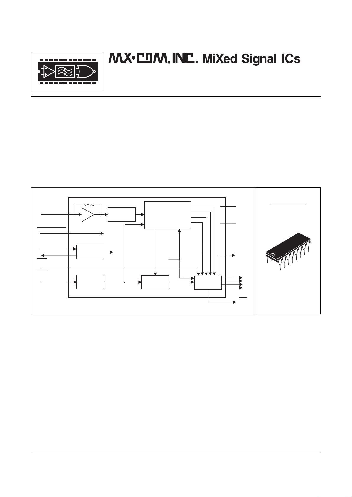
The MX623 is a low-power decoding integrated circuit that measures the frequency of telephone system call progress
tones.
With progress signals input from the telephone line, this single-chip product is programmed to recognize up to thirteen
of the World's most commonly used call-progress frequencies, analyze signal quality, and present the measured result
as a 4-bit parallel data word at the tri-state Data Output.
Using the parallel information from the MX623, the host system, can recognize such call progress information as: ‘Dial’,
‘Busy’, ‘Number Unobtainable’, ‘Ringing’ and Fax/Modem system signals.
This information can then be used in simple or complex applications to control telephone operations. The data output
will require a software format that can analyze the frequency information from the MX623.
Requiring only a single 3.0
[MIN]
volt power supply, the MX623 may be line-powered and will operate under simple logic
or system µProcessor control using the 'Data-Change, 'Hold' and 'Chip-Select' functions.
The MX623, whose small size and low power consumption makes it ideal for remote applications, requires a
3.579545MHz telephone system clock or Xtal input, is available in a 16-pin PDIP.
AVAILABLE
PACKAGES
MX623P
16-pin PDIP
XTAL/CLOCK
OSCILLATOR
SIGNAL IN
XTAL/CLOCK
Clocks
Clocks
DATA
CHANGE
DATA
OUTPUTS
Q0
Q1
Q2
Q3
IRQ
V
DD
V
SS
CONTROL
CIRCUITRY
TIMER
CHIP SELECT
HOLD
PURS
DIGITAL
FIL TER
OUTPUT
LATCHES
LIMITER
XTAL
MEASUREMENT
AND
DECODE
• MX•COM MiXed Signal CMOS
• Custom Tone Decoder (13 Call-Progress
Frequencies Recognized)
• Operates to a 3.579545MHz Telephone System
Clock
• Operates Under Simple Logic or µProcessor
System Control
• Measures Call Progress Tone Frequencies
(‘Busy’, ‘Dial’, ‘Fax-Tone’ etc.)
• Telephone, PABX, Fax and Dial-Up Modem
Applications
• Low-Power Requirement (600µA at 3.3 Volts
TYP
)
for Line-Powered Applications
Line-Powered Call Progress
Tone Detector
© 1997 MX•COM Inc. www.mxcom.com Tele: 800 638-5577 910 744-5050 Fax: 910 744-5054 Doc. # 20480091.003
4800 Bethania Station Road, Winston-Salem, NC 27105-1201 USA All trademarks and service marks are held by their respective companies.

© 1997 MX•COM Inc. www.mxcom.com Tele: 800 638-5577 910 744-5050 Fax: 910 744-5054 Doc. # 20480091.003
4800 Bethania Station Road, Winston-Salem, NC 27105-1201 USA All trademarks and service marks are held by their respective companies.
Line- Powered Call Progress Detector 2 MX623 Preliminary Information
Q3:
Q2:
Q1:
Q0:
VDD: Positive supply rail. A minimum supply voltage of 3.0 volts is required. Levels and voltages
within this decoder are dependent upon this supply.
Signal In: The composite audio input. Signals to this pin should be a.c. coupled. The d.c. bias of
the limiter section is set internally; this pin should not be loaded with any other circuitry.
No internal connection. Leave open circuit.
Xtal: The output of the on-chip clock oscillator inverter.
No internal connection. Leave open circuit.
Xtal/Clock: The input to the clock oscillator inverter. A 3.579545MHz Xtal or externally derived
clock should be connected here (see Figure 2).
VSS: Negative supply rail (GND).
Hold: An input to control the Output Latch condition; employed in combination with the Data
Change output to facilitate, if required, Interrupt and/or handshake operations with a µProcessor.
With Hold placed “Low”, with a tone input, the Data Change output will be held “High” at the next
data change, and the current output code is locked in the Output Latches regardless of any
changes to the input signal. The output code remains as held until this input is returned “High”
(see Figure 3). While this input is “High” the output data, Q0 - Q3, cycles normally with the input
audio. This pin has an internal 1.0MΩ pullup resistor.
PURS: Power-Up ReSet. To reset internal circuitry at power-up; a logic “1” level is required at this
pin for a duration of at least 2.5ms after the Xtal/Clock input and full VDD levels are applied. The
component configuration shown in Figure 2 is recommended; for slow-rising power supplies the
time constant of components should be increased accordingly.
IRQ: Interrupt Request. An output for µProcessor operation; normally “High” this output is latched
“Low” when an internal data change occurs if the Chip Select input is “High”. This output is reset
(“High”) the when Chip Select line is taken “Low”. To permit “wire-OR” connection with other
peripherals, this output has a low-impedance when “Low” and a high-impedance when “High”.
CS: Chip Select- A controlling function. When held “High” the Data Outputs Q0, Q1, Q2 and Q3
and the Data Change output are disabled. When taken “Low” the Data Outputs Q0, Q1, Q2 and
Q3 and the Data Change output are enabled; the Interrupt Request (IRQ) is reset (“High”) when
CS is taken “Low”. See Figures 3 and 4.
Data Change: A positive-going pulse is generated at this output when the data changes (Tone or
NOTONE). New tone-data is presented to the Q0, Q1, Q2 and Q3 Data Outputs if the Hold input is
set “High”. This is a tri-state output.
1
2
3
4
5
6
7
8
9
10
11
12
13
14
15
16
Data Outputs: A 4-bit parallel data word, forming a HEX character representing the decoded
tone frequency. This word is output after a successful decode. Table 1 details the Hex
character output codes for the relevant decoded tone frequencies. Upon power-up this output
is set to ‘EH’, but no Data Change pulse generated. These are tri-state outputs.
Pin Function
 Loading...