

MX COM Inc MX619J, MX619LH, MX619P Datasheet
COMMUNICATION ICs
DATA BULLETIN
MX619
Delta Modulation Codec
meets EUROCOM D1-IA8
2000 MX-COM, Inc. www.mxcom.co m Tel: 800 638 5577 336 744 5050 Fax: 336 744 5054 Doc. # 20480189.002
4800 Bethania Station Road, Winston-Salem, NC 27105-1201 USA All Trademarks and service marks are held by their respective companies.
Features Applications
•
Meets EUROCOM D1-IA8
•
Single Chip Full Duplex CVSD CODEC
•
On-chip Input and Output Filters
•
Programmable Sampling Clocks
•
3- or 4-bit Companding Algorithm
•
Powersave Capabilities
•
Low Power, 5.0V Operation
•
Military Communications
•
Multiplexers, Switches, & Phones
➤
➤
➤
➤
➤
➤
➤
➤
➤
➤
➤
➤➤
➤
➤
➤
➤
➤➤
➤
➤
➤
➤
➤
➤
➤
➤
➤
The MX619 is a Continuously Variable Slope Delta Modulation (CVSD) Codec designed for use in military
communications systems. This device is suitable for applications in military delta multiplexers, switches, and
phones. The MX619 is designed to meet EUROCOM D1-IA8 specifications.
Encoder input and decoder output filters are incorporated on-chip. Sampling clock rates can be programmed
to 16, 32, or 64kbps from an internal clock generator or externally injected in the 8 to 64kbps range. The
sampling clock frequency is output for the synchronization of external circuits.
The encoder has an enable function for use in multiplexer applications. Encoder and Decoder forced idle
capabilities are provided forcing 10101010…pattern in encode and a V
DD
/2 bias in decode. The companding
circuit may be operated with an externally selectable 3- or 4-bit algorithm. The device may be placed in
standby mode by selecting Powersave. A reference 1.024MHz oscillator uses an external clock or crystal.
The MX619 operates with a supply voltage of 5.0V and is available in the following packages: 24-pin PLCC
(MX619LH), 22-pin CERDIP (MX619J), and 22-pin PDIP (MX619P).

Delta Modulation CODEC 2 MX619
2000 MX-COM, Inc. www.mxcom.com Tel: 800 638 5577 336 744 5050 Fax: 336 744 5054 Doc. # 20480189.002
4800 Bethania Station Road, Winston-Salem, NC 27105-1201 USA All Trademarks and service marks are held by their respective companies.
CONTENTS
Section Page
1 Block Diagram................................................................................................................3
2 Signal List.......................................................................................................................4
3 External Components....................................................................................................6
4 General Description.......................................................................................................6
5 Application .....................................................................................................................7
5.1 CODEC Integration.............................................................................................................. 7
5.2 Digital to Analog Performance............................................................................................. 7
6 Performance Specification..........................................................................................11
6.1 Electrical Performance...................................................................................................... 11
6.1.1 Absolute Maximum Ratings..................................................................................................11
6.1.2 Operating Limits...................................................................................................................11
6.1.3 Operating Characteristics.....................................................................................................12
6.1.4 TIMING.................................................................................................................................13
6.2 Packaging.......................................................................................................................... 14
MX-COM, Inc. reserves the right to change specifications at any time and without notice.
Delta Modulation CODEC 3 MX619
2000 MX-COM, Inc. www.mxcom.com Tel: 800 638 5577 336 744 5050 Fax: 336 744 5054 Doc. # 20480189.002
4800 Bethania Station Road, Winston-Salem, NC 27105-1201 USA All Trademarks and service marks are held by their respective companies.
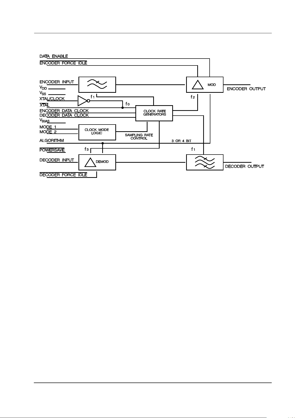
1 Block Diagram
➤
➤
➤
➤
➤
➤
➤
➤
➤
➤
➤
➤➤
➤
➤
➤
➤
➤➤
➤
➤
➤
➤
➤
➤
➤
➤
➤
Figure 1: Block Diagram
Delta Modulation CODEC 4 MX619
2000 MX-COM, Inc. www.mxcom.com Tel: 800 638 5577 336 744 5050 Fax: 336 744 5054 Doc. # 20480189.002
4800 Bethania Station Road, Winston-Salem, NC 27105-1201 USA All Trademarks and service marks are held by their respective companies.
2 Signal List
J/P LH Name Signal Description
1 1 Xtal/Clock input Input to the clock oscillator inverter. A 1.024MHz Xtal input or
externally derived clock is injected here. See Clock Mode pins
and Figure 2.
2 N/C No Connection
2 3
Xtal
output The 1.024 MHz output of the clock oscillator inverter.
3 4 N/C No Connection
4 5 Encoder Data
Clock
input/
output
A logic I/O port. External encode clock input or internal data
clock output. Clock frequency is dependent upon Clock Mode 1,
2 inputs and Xtal frequency (see Clock Mode pins).
5 6 Encoder Output output The encoder digital output. This is a three-state output whose
condition is set by the Data Enable and
Powersave inputs. See
Table 2.
6 7
Idle Force Encoder
When this pin is at a logical “0” the encoder is forced to an idle
state and the encoder digital output is 0101, a perfect idle
pattern. When this pin is a logical “1” the encoder encodes as
normal. Internal 1MΩ pullup.
7 8 Data Enable input Data is made available at the encoder output pin by control of
this input. See Encoder Output pin. Internal 1 MΩ pullup.
8 9 N/C No Connection
9 10 V
BIAS
Normally at VDD/2 bias, this pin should be externally decoupled
by capacitor C4. Internally pulled to V
SS
when “
Powersave
” is
a logical “0”.
10 11 Encoder Input input The analog signal input. Internally biased at VDD/2, this input
requires an external coupling capacitor. The source impedance
should be less than 100Ω. Output channel noise levels will
improve with an even lower source impedance. See Figure 2.
11 12 VSS power Negative Supply
12 13 N/C No Connection
13 14 Decoder Output output The recovered analog signal is output at this pin. It is the
buffered output of a lowpass filter and requires external
components. During “Powersave” this output is open circuit.
14 15 N/C No Connection
15 16
Powersave
A logic “0” at this pin puts most parts of the codec into a
quiescent non-operational state. When at a logical “1”, the
codec operates normally. Internal 1 MΩ pullup.
17 N/C No Connection
16 18
Idle Force Decoder
A logic “0” at this pin gates a 0101... pattern internally to the
decoder so that the Decoder Output goes to V
DD
/2. When this
pin is a logical “1” the decoder operates as normal. Internal
1MΩ pullup.
17 19 Decoder Input
The received digital signal input. Internal 1 MΩ pullup.
18 20 Decoder Data
Clock
input/
output
A logic I/O port. External decode clock input or internal data
clock output, dependent upon clock mode 1,2 inputs. See Clock
Mode pins.
19 21 Algorithm A logic “1” at this pin sets this device for a 3-bit companding
algorithm. A logical “0” sets a 4-bit companding algorithm.
Internal 1 MΩ pullup.
Delta Modulation CODEC 5 MX619
2000 MX-COM, Inc. www.mxcom.com Tel: 800 638 5577 336 744 5050 Fax: 336 744 5054 Doc. # 20480189.002
4800 Bethania Station Road, Winston-Salem, NC 27105-1201 USA All Trademarks and service marks are held by their respective companies.
J/P LH Name Signal Description
20 22 Clock Mode 2
21 23 Clock Mode 1
Clock rates refer to f = 1024MHz Xtal/Clock input. During
internal operation the data clock frequencies are available at
the ports for external circuit synchronization. Independent or
common data rate inputs to Encode and Decode data clock
ports may be employed in the External Clocks mode. Internal
1MΩ pullups. See Table 3.
22 24 VDD power Positive Supply. A single 5.0V supply is required.
Table 1: Signal List
Data Enable Powersave Encoder Output
1 1 Enable
0 1 High Z (open circuit)
1 0 VSS
Table 2: Encoder Output
Clock Mode 1 Clock Mode 2 Facility
0 0 External Clocks
0 1 Internal, 64kbps = f/16
1 0 Internal, 32kbps = f/32
1 1 Internal, 16kbps = f/64
Table 3: Clock Mode
 Loading...