DATA BULLETIN
MX613
MXCOM MiXed Signal CMOS
Covers Worldwide Call Progress Frequencies
(300Hz TO 2150Hz)
Decode Single or Modulated Tones
SERIAL CLOCK
CHIP SELECT
V
DD
SIGNAL IN
LEVEL IN
V
SS
XTAL/CLOCK
3.579545MHz
XTAL
LEVEL
DETECTOR
f/4
BAND SELECTOR
SIGNAL QUALITY
ASSESSOR
CLOCK
GENERATOR
FILTER &
HI / BANDLO
RESET
CS
f
f/4
GOOD/BAD
HI/LO
HI/LO
DECODE
ON / OFF
LOGIC
TIMER
LO = 39.4ms
HI = 13.16ms
COUNT
RESET
CS
Global Call Progress Detector
PRELIMINARY INFORMATION
Analog In / Serial Data Out
µProcessor Compatible Outputs
Speech Discrimination Ability
Low Power Operation
SERIAL OUTPUT
PORT (6-BITS)
LATC H
FREQUENCY
COUNTER
RESET
TIME
DAT A OUT
012345
TIME
V
IRQ
AVAILABLE
PACKAGES
MX613DW
16-pin SOIC
BIAS
14-pin PDIP
MX613P
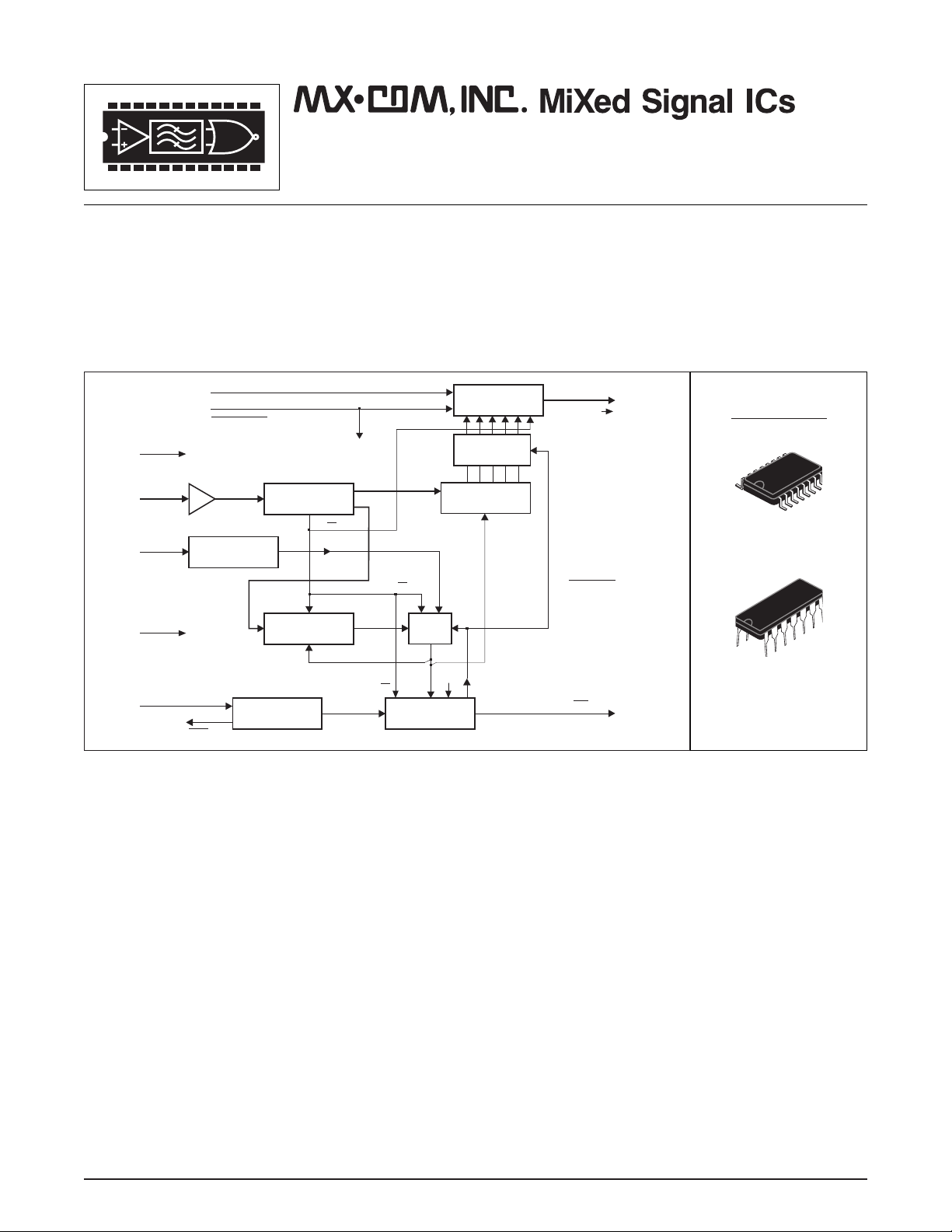
The MX613 is a wide-band, ‘N-Tone’ non-predictive tone decoder that measures telephone system call progress
tones in PABX, Pay/Feature-Phone, Fax and Modem systems.
Adhering to Must/Must-Not Decode limits and able to measure inband frequencies in outband modulation, this
decoder measures the frequency of input signals in the range 300 to 2,150Hz. The result of each measurement is
presented to a system µProcessor as a 6-bit serial word.
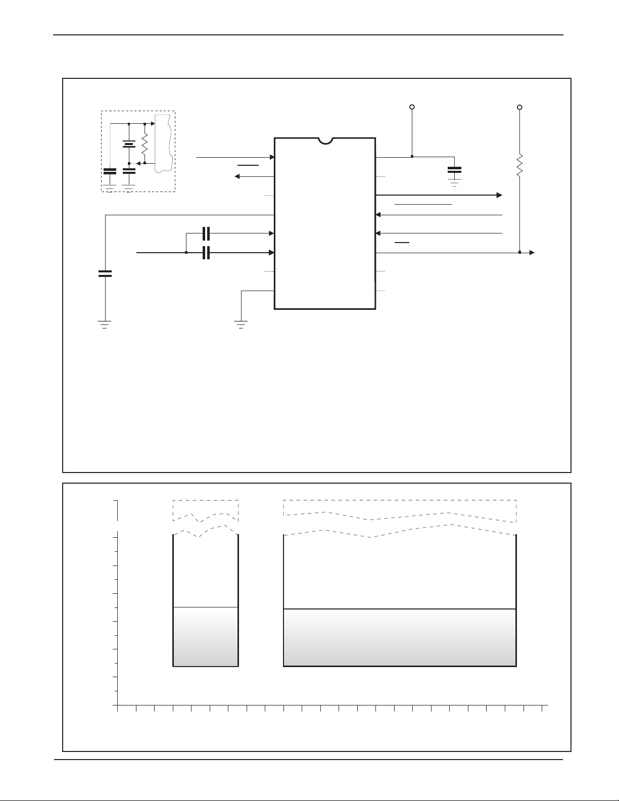
The decode frequency range, which covers the world's call progress application spectrum, is processed internally
as two bands: LO = 300 to 660Hz and HI = 900 to 2150Hz. Frequency measurement is achieved by counting the
number of cycles in a set time period
(LO = 39.47ms or HI = 13.16ms). Bad signal/level quality or NOTONE results in a count-abort, timing-reset and no
output from the decoder.
Front-end filtering is achieved using our patented Auto-Correlator. Current frequency information is output for the
µProcessor using a Serial Data, Clock and Interrupt interface.
Data from the MX613 should be processed by a µProcessor whose algorithms are able to recognize the
frequency, sequence and/or cadence of input signals as national call progress information; e.g.: ‘Dial,’ ‘Busy,’
‘Number-Unobtainable,’ ‘Ringing’ and automatic tones used by fax and modem systems. Software can be simply
configured to reject speech frequencies.
Available in SOIC and PDIP packages, this low-cost, mixed signal IC has a typical power requirement of less
than 1mA at 3 volts and utilizes a telecom-system clock input of 3.579545MHz to maintain frequency accuracy.
© 1997 MX•COM Inc. www.mxcom.com Tele: 800 638-5577 910 744-5050 Fax: 910 744-5054 Doc. # 20480086.003
4800 Bethania Station Road, Winston-Salem, NC 27105-1201 USAAll trademarks and service marks are held by their respective companies

Global Call Progress Tone Detector 2 MX613 Preliminary Information
Pin Number Function
MX613DW
1
2
3
4
5
6
MX613P
1
2
3
4
5
6
Xtal/Clock: The input to the on-chip clock oscillator inverter. A 3.579545MHz Xtal or
externally derived telephone system clock (f
) should be connected here. Operation
XTAL
of the MX613 without a suitable Xtal/Clock input may cause device damage.
Xtal: The output of the on-chip clock oscillator inverter. See Figure 2.
No internal connection.
V
: The internal circuitry bias line, held at VDD/2 this pin must be decoupled to VSS.
BIAS
Level In: The input for level discrimination. This input is internally biased to V
. Signals
BIAS
must be a.c. coupled, and the audio signal must be fed to both this pin and the Signal In
pin. Correct level detection determines the operation of this device (see Principles of
Decoder Operation). But if you wish to disregard the amplitude of the input levels, the
MX613 may be permanently enabled by pulling this pin to VDD and disabled by pulling to
VSS.
Signal In: The input for frequency discrimination and decoding. This input is internally
biased to V
. Signals must be a.c. coupled. The audio signal must be fed to both this
BIAS
pin and the Level In pin.
7
8
9
10
11
12
13
14
7
8
9
10
11
12
No internal connection.
VSS: Signal ground (GND).
No internal connection.
No internal connection.
IRQ: This Interrupt Request output from the MX613 is ‘wire-OR able’ allowing the
interrupt outputs of other peripherals to be combined and connected to the Interrupt input
of a µProcessor. This input has a low-impedance pulldown to V
when active and a high-
SS
impedance when inactive. An interrupt is produced on completion of a HI or LO frequency
measurement.
Serial Clock: The serial clock from the µProcessor. Data Out is clocked into the
µProcessor on the rising edge of the Serial Clock. See Data-Read Timing diagram.
Chip Select: A logic “0” at this input will select this device.
Data Out: The serial data output. Under the control of the Chip Select and Serial Clock
inputs, data should be read from this output in 6-bit blocks MSB (Bit-5) first.
If 8 serial clock pulses are applied, two additional logic “0s” will be output after Bit-0.
15
16
13
14
No internal connection.
VDD: Positive supply input. A single, stable supply is required. Levels and voltages within
the MX613 are dependent upon this supply. This pin should be decoupled to VSS by a
capacitor located close to the MX613 pins.
© 1997 MX•COM Inc. www.mxcom.com Tele: 800 638-5577 910 744-5050 Fax: 910 744-5054 Doc. # 20480086.003
4800 Bethania Station Road, Winston-Salem, NC 27105-1201 USAAll trademarks and service marks are held by their respective companies

Global Call Progress Tone Detector 3 MX613 Preliminary Information
Application Information
1
R
2
X
1
C
5
2
C
6
XT AL/CLOCK
XT AL
1
2
3
V
AUDIO SIGNAL
C
2
C
1
BIAS
LEVEL IN
SIGNAL IN
4
5
6
7
C
3
Notes
(1) The Xtal/Clock input may be driven from the host telephone
system's 3.579545MHz clock; if a Xtal drive is required, the
configuration shown in the INSET is recommended.
(2) The audio signal should be input to both Signal In and Level In
pins via separate coupling capacitors. If it is wished to operate
the device with disregard to on-chip level thresholds and
permanently enable the MX613, the Level In pin should be held
at VDD.
To disable the MX613 the Level In pin should be held at VSS.
Level thresholds are preset internally.
V
SS
8
Figure 2 - External Component Connections
MX613DW
V
DD
V
16
15
14
13
12
11
DD
C
4
DAT A OUT
CHIP SELECT
SERIAL CLOCK INPUT
IRQ
10
9
Component Value
R
1
R
2
C
1
C
2
C
3
C
4
C
5
C
6
X
1
Tolerances: C = ± 20% R = ± 10%
3.579545MHz
R
22.0kΩ
1.0MΩ
0.01µF
0.1µF
1.0µF
1.0µF
33.0pF
33.0pF
V
DD
1
V
DD
775mVrms
0
-10
-20
Low Band
(LO)
High Band
(HI)
Must
Decode
-30
Level (dB)
-40
Must-Not
Decode
-50
0
200 400 600 800 1000 1200 1400 1600 1800 2000 2200
Frequency (Hz)
Figure 3 - HI/LO Decode Bands
© 1997 MX•COM Inc. www.mxcom.com Tele: 800 638-5577 910 744-5050 Fax: 910 744-5054 Doc. # 20480086.003
4800 Bethania Station Road, Winston-Salem, NC 27105-1201 USAAll trademarks and service marks are held by their respective companies
 Loading...