

MX COM Inc MX612E3, MX612P6 Datasheet
COMMUNICATION ICs
DATA BULLETIN
CMX612
Calling Line Identifier
with VMWI
¤1999 MX-COM, Inc. www.mxcom.com tel: 800 638 5577 336 744 5050 fax: 336 744 5054 Doc. # 20480202.002
4800 Bethania Station Road, Winston-Salem, NC 27105-1201 USA All trademarks and service marks are held by their respective companies.
ADVANCE INFORMATION
Features Applications
x
CLI, CIDCW and VMWI System Operation
x
CLASS (FSK) and SDT (Stuttered Dial Tone)
x
Low Power Operation 0.5mA at 2.7V
x
Zero-Power Detector for Ring or Line
Reversal
x
Low CAS Tone Falsing in CIDCW Mode
x
Bellcore, British Telecom, ETSI, and
Mercury Compatible
x
CLI and CIDCW Adjunct Boxes
x
CLI and CIDCW Feature Phones
x
Computer Telephony Integration
x
Call Logging Systems
x
Voice-Mail Equipment
-
+
XTAL
XTAL
+
Bandpass
Filters
FSK
Demod
Level
Detector
Detect
Mode
Tone Alert
Detector
Dial Tone
Detector
Data
Retiming
Mode
Control
Logic
RXD
RXCLK
IRQ
IN1-
IN2-
IN1+
IN2+
AMPOUT1
AMPOUT2
Power
Supply
Circuits
Xtal Osc and
Clock Dividers
DET
RD
RT
V
DD
V
BIAS
V
SS
MODE 2
MODE 1
INPUT SELECT
The CMX612 is a low power CMOS device used for the reception of physical layer signals in Bellcore’s
Calling Identity Delivery system (CID), British Telecom’s Calling Line Identification Service (CLIP), the Cable
Communications Association’s Caller Display Services (CDS), and similar evolving systems. This device also
meets the requirements of emerging Caller Identity with Call Waiting Services (CIDCW).
Visual Message Waiting Indicator (VMWI) detection in both CLASS (FSK) and (SDT) Stuttered Dial Tone
modes is provided by the CMX612. In addition, two different signal inputs are available to support Tip/Ring
and Hybrid connectivity. This device includes a ‘zero-power’ ring or line reversal detector, two dual-tone
detectors and a 1200-baud FSK Bell 202/V.23 compatible asynchronous data demodulator. The dual-tone
detectors are the Tone Alert Signal (2130Hz plus 2750Hz) detector and the stuttered dial tone (350Hz plus
440Hz) detector. The 1200-baud FSK Bell 202/V.23 compatible asynchronous data demodulator with data
retiming circuitry removes the need for a UART in the associated
P
C.
The CMX612 is suitable for use in systems using Bellcore specifications GR-30-CORE and SR-TSV-002476,
British Telecom specifications SIN227 and SIN242, CCA TW/P&E/312, ETSI ETS 300 659 parts 1 and 2, ETS
300 778 parts 1 and 2, and Mercury Communications MNR 19.
This device may be used with a 2.7V to 5.5V power supply and is available in the following packages:
20-pin TSSOP (CMX612E3) or 22-pin PDIP (CMX612P6).

Calling Line Identifier with VMWI 2 CMX612 Advance Information
¤1999 MX-COM, Inc. www.mxcom.com tel: 800 638 5577 336 744 5050 fax: 336 744 5054 Doc. # 20480202.002
4800 Bethania Station Road, Winston-Salem, NC 27105-1201 USA All trademarks and service marks are held by their respective companies.
CONTENTS
Section Page
1 Block Diagram................................................................................................................3
2 Signal List.......................................................................................................................4
3 External Components....................................................................................................5
4 General Description.......................................................................................................6
4.1 Mode Control Logic ............................................................................................................. 6
4.2 Input Signal Amplifiers......................................................................................................... 7
4.3 Bandpass Filters.................................................................................................................. 8
4.4 Level Detector ..................................................................................................................... 8
4.5 FSK Demodulator................................................................................................................ 8
4.6 FSK Data Retiming.............................................................................................................. 9
4.7 Tone Alert Detector ........................................................................................................... 10
4.8 Dial Tone Detector............................................................................................................. 11
4.9 Ring or Line Polarity Reversal Detector ............................................................................ 11
4.10 Xtal Osc and Clock Dividers.............................................................................................. 12
5 Application Notes ........................................................................................................13
5.1 'On-Hook' Operation..........................................................................................................13
5.1.1 Bellcore System ...................................................................................................................13
5.1.2 British Telecom System........................................................................................................13
5.1.3 Other On-hook Systems.......................................................................................................14
5.2 'Off-Hook' Operation.......................................................................................................... 16
5.3 VMWI Operation................................................................................................................ 18
5.3.1 SDT Mode............................................................................................................................18
5.3.2 CLASS (FSK) Mode.............................................................................................................18
6 Performance Specification..........................................................................................20
6.1 Electrical Performance ...................................................................................................... 20
6.1.1 Absolute Maximum Ratings..................................................................................................20
6.1.2 Operating Limits...................................................................................................................20
6.1.3 Operating Characteristics.....................................................................................................21
6.2 Packaging.......................................................................................................................... 24
MX-COM, Inc. reserves the right to change specifications at anytime and without notice.
Calling Line Identifier with VMWI 3 CMX612 Advance Information
¤1999 MX-COM, Inc. www.mxcom.com tel: 800 638 5577 336 744 5050 fax: 336 744 5054 Doc. # 20480202.002
4800 Bethania Station Road, Winston-Salem, NC 27105-1201 USA All trademarks and service marks are held by their respective companies.
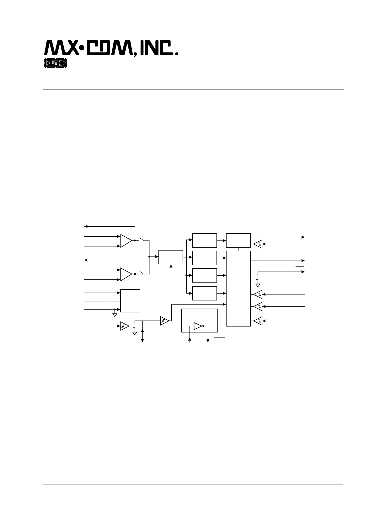
1 Block Diagram
-
+
XTAL
XTAL
-
+
Bandpass
Filters
FSK
Demod
Level
Detector
Detect
Mode
Tone Alert
Detector
Dial T one
Detector
Data
Retiming
Mode
Control
Logic
RXD
To / From µC
RXCLK
IRQ
IN1-
IN2-
IN1+
IN2+
AMPOUT1
Tip & Ring
Hybrid
Rx Output
AMPOUT2
C8
C9
R5
C5
C2
C1
X1
Power
Supply
Circuits
Xtal Osc and
Clock Dividers
DET
RD
RT
V
DD
V
BIAS
V
SS
V
DD
3.579545MHz
MODE 2
MODE 1
INPUT SELECT
Figure 1: Block Diagram

Calling Line Identifier with VMWI 4 CMX612 Advance Information
¤1999 MX-COM, Inc. www.mxcom.com tel: 800 638 5577 336 744 5050 fax: 336 744 5054 Doc. # 20480202.002
4800 Bethania Station Road, Winston-Salem, NC 27105-1201 USA All trademarks and service marks are held by their respective companies.
2 Signal List
Package Signal
E3 P6 Name Type
Description
11
XTAL
output The output of the on-chip Xtal oscillator inverter.
2 2 XTAL input The input to the on-chip Xtal oscillator inverter.
3 3 RD input (S) Input to the Ring or Line Polarity Reversal Detector.
4 4 RT bi-directional Open-drain output and Schmitt trigger input forming part of the
Ring or Line Polarity Reversal detector. An external resistor
to V
DD
and a capacitor to VSS should be connected to RT to
filter and extend the RD input signal.
55 INPUT
SELECT
input (S) Controls the selection of the two Input Signal Amplifiers. A
low level selects Input 1 and a high level selects Input 2.
6 6 AMPOUT1 bi-directional The output of on-chip Input Signal Amplifier 1 and an input to
the signal selection multiplexer.
7 7 IN1- input The inverting input to on-chip Input Signal Amplifier 1.
8 8 IN1+ input The non-inverting input to on-chip Input Signal Amplifier 1.
910 V
BIAS
output Internally generated bias voltage, held at VDD/2 when the
device is not in ‘Zero-Power’ mode. Should be bypassed to
V
SS
by a capacitor mounted close to the device pins.
10 11 V
SS
Power Negative supply rail (signal ground).
11 12 IN2+ input The non-inverting input to on-chip Input Signal Amplifier 2.
12 13 IN2- input The inverting input to on-chip Input Signal Amplifier 2.
13 14 AMPOUT2 bi-directional
The output of on-chip Input Signal Amplifier 2 and an input to
the signal selection multiplexer.
14 15 MODE 2 input (S) Input used to select the operating mode. See Section 4.1.
15 16 MODE 1 input (S) As per MODE 2 description.
16 17
IRQ
output An open-drain active low output that may be used as an
Interrupt Request/Wake-up input to the associated PC. An
external pull-up resistor should be connected between this
output and V
DD
.
17 18 DET output
A logic level output driven by the Ring or Line Polarity
Reversal Detector, the Tone Alert Detector, the Dial Tone
Detector or the FSK Level detect circuits, depending on the
operating mode. See Section 4.1.
18 19 RXCLK input (S)
An input that may be used to clock received data bits out of
the FSK Data Retiming block.
19 21 RXD output A logic level output carrying either the raw output of the FSK
Demodulator or re-timed 8-bit characters depending on the
state of the RXCLK input. See Section 4.6
20 22 V
DD
Power The positive supply rail. Levels and thresholds within the
device are proportional to this voltage. Should be bypassed
to V
SS
by a capacitor mounted close to the device pins.
9, 20 Not used. Do not connect to these pins.
Input (S) = Schmitt Trigger Input
Table 1: Signal List
Calling Line Identifier with VMWI 5 CMX612 Advance Information
¤1999 MX-COM, Inc. www.mxcom.com tel: 800 638 5577 336 744 5050 fax: 336 744 5054 Doc. # 20480202.002
4800 Bethania Station Road, Winston-Salem, NC 27105-1201 USA All trademarks and service marks are held by their respective companies.
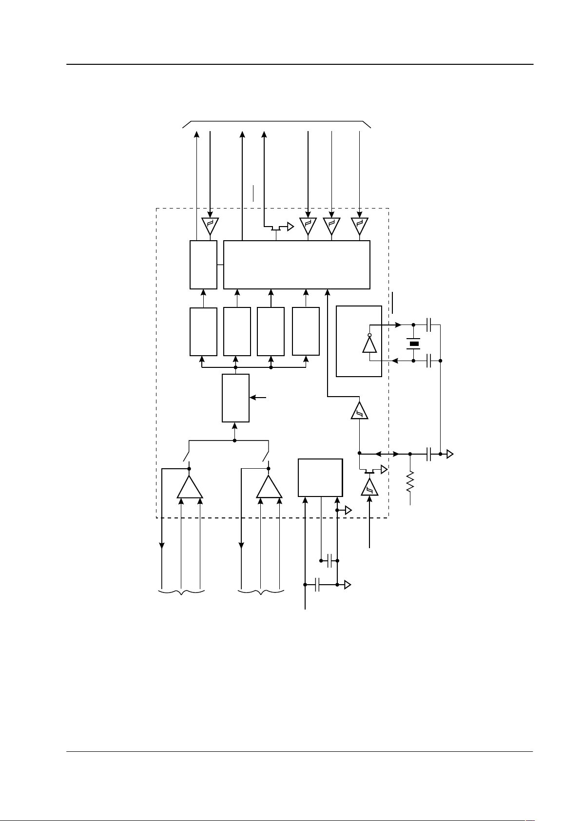
3 External Components
Tip & Ring
20
19
18
17
16
15
10
13
12
11
14
1
2
3
4
5
6
7
8
9
XTAL
XTAL
V
DD
V
SS
V
BIAS
V
BIAS
V
BIAS
IN1+
IN2+
INPUT SELECT
IN1-
IN2-
RD
RT
RXD
RXCLK
DET
IRQ
MODE 1
MODE 2
X1
R1
R2
R3
R4
R5
R8
R6
R7
R9 R10
R13
R12
R11
R17
R16
1:1
2-Wire
Line
R15
R14
R18
D1 - 4
C3
C2
C1
C4
C5
C6
C7
C14
RELAY DRIVER
LOUDSPEAKER
MIC
C13 C12
C11
C8
C9
V
DD
V
DD
V
DD
To/From µC
From µC
Line
Protection
Network
A
B
CMX
612
AMPOUT1
AMPOUT2
Figure 2: Recommended External Components Typical Application
R1
470k
:
C1, C2 18pF
R2 See Section 4.8 C3, C4
0.1PF
R3 – R7
470k
:
C5
0.33PF
R8 Note 1
470k: for V
DD
= 3.3V
680k: for V
DD
= 5.0V
C6, C7 680pF
R9 Note 1
240k: for V
DD
= 3.3V
200k: for V
DD
= 5.0V
C8, C9 Note 2
0.1PF
R10
160k
:
C11, C12 330pF
R11 - R14
100k
:
C13 10nF
R15
600
:
C14 100nF
R16
120k
:
R17
100k
:
X1 Note 3 3.579545MHz
R18
100k: r20%
D1 - D4 1N4004
Resistors r1%, capacitors r20% unless otherwise stated.
Table 2: Recommended External Components for Typical Application

Calling Line Identifier with VMWI 6 CMX612 Advance Information
¤1999 MX-COM, Inc. www.mxcom.com tel: 800 638 5577 336 744 5050 fax: 336 744 5054 Doc. # 20480202.002
4800 Bethania Station Road, Winston-Salem, NC 27105-1201 USA All trademarks and service marks are held by their respective companies.
Recommended External Components Notes:
1. Reference Section 4.2
2. It is recommended that the printed circuit board be laid out with a ground plane in the CMX612 area to
provide a low impedance ground connection to the V
SS
pin and to the decoupling capacitors C8 and C9.
3. For best results, a crystal oscillator design should drive the clock inverter input with signal levels of at
least 40% of V
DD
, peak to peak. Tuning fork crystals generally cannot meet this requirement. To obtain
crystal oscillator design assistance, please consult you crystal manufacturer.
4 General Description
4.1 Mode Control Logic
The CMX612's operating mode and the source of the DET and
IRQ
outputs are determined by the logic levels
applied to the MODE 1 and MODE 2 input pins;
MODE 1 MODE 2 Mode DET output from
IRQ
output from
0 0 Tone Alert Detect Tone Alert Signal Detection.
CAS tones present.
Valid ‘off-hook’ CAS or
Ring or Line Polarity
Reversal Detection.
Ringing Signal present.
0 1 FSK Receive FSK Level Detection.
FSK present.
FSK Data Retiming [1] or
Ring or Line Polarity
Reversal Detection.
Ringing Signal present.
1 0 'Zero-Power' Ring or Line Polarity Reversal
Detection.
Ringing Signal present.
Ring or Line Polarity
Reversal Detection.
Ringing Signal present.
1 1 Dial Tone Detect Dial Tone Signal Detection.
Both tones present.
Valid dial tone detected.
[1]
If enabled.
In 'Zero-Power' mode, power is removed from all of the internal circuitry except for the Ring or Line Polarity
Reversal Detector and the DET and
IRQ
outputs.
Calling Line Identifier with VMWI 7 CMX612 Advance Information
¤1999 MX-COM, Inc. www.mxcom.com tel: 800 638 5577 336 744 5050 fax: 336 744 5054 Doc. # 20480202.002
4800 Bethania Station Road, Winston-Salem, NC 27105-1201 USA All trademarks and service marks are held by their respective companies.
4.2 Input Signal Amplifiers
These amplifiers can be used to convert the balanced FSK, Tone Alert and VMWI signals received over the
telephone line to an unbalanced signal of the correct amplitude for the FSK receiver, Tone Alert and Dial
Tone Detector circuits.
-
+
V
SS
V
BIAS
AMPOUT
IN+
IN-
R8R6
R7
R9 R10
C6
C7
C9
A
B
Input Signal Amplifier
Figure 3: Input Signal Amplifier, balanced input configuration
The design equations for this circuit are;
()
10R-8R
10R
×8R=9R
k160=R10
k470=7R=6R
R9
R8
=
)A-B(V
V
g
ain voltage alDifferenti
AMPOUT
c
c
The target differential voltage gain depends on the expected signal levels between the A and B wires and the
CMX612's internal threshold levels, which are proportional to the supply voltage.
The CMX612 has been designed to meet the applicable specifications with R8 = 430k: at V
DD
= 3.0V
nominal, rising to 680k: at V
DD
= 5.0V, and R9 should be 240k: at V
DD
= 3.0V and 200k: at V
DD
= 5.0V as
shown in Section 3 and Figure 5.
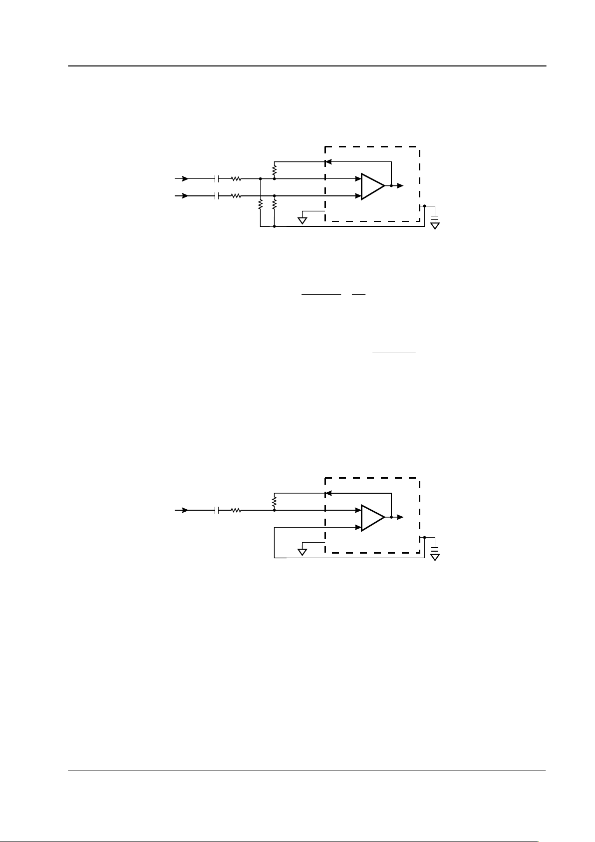
The Input Signal Amplifiers may also be used with an unbalanced signal source as shown in Figure 4. The
values of R6 and R8 are as for the balanced input case.
-
+
V
SS
V
BIAS
AMPOUT
IN+
IN-
R8R6
C6
C9
A
Input Signal Amplifier
Figure 4: Input Signal Amplifier, unbalanced input configuration
Calling Line Identifier with VMWI 8 CMX612 Advance Information
¤1999 MX-COM, Inc. www.mxcom.com tel: 800 638 5577 336 744 5050 fax: 336 744 5054 Doc. # 20480202.002
4800 Bethania Station Road, Winston-Salem, NC 27105-1201 USA All trademarks and service marks are held by their respective companies.
0
100
200
300
400
500
600
700
800
900
1000
33.544.55
Nominal V (V)
DD
R8
R9
R8 and R9 : k W
Figure 5: Input Signal Amplifier, optimum values of R8 and R9 vs. V
DD
4.3 Bandpass Filters
These are used to attenuate out of band noise and interfering signals which might otherwise reach the FSK
Demodulator, Tone Alert Detector, Dial Tone detector and Level Detector circuits. The characteristics of
these filters differ in FSK, Tone Alert and Dial Tone modes. Most of the filtering is provided by switched
capacitor stages clocked at 57.7kHz or 9.62kHz depending on mode of operation.
4.4 Level Detector
This block operates by measuring the level of the signal at the output of the Bandpass Filter, and comparing it
against a threshold that depends on whether FSK Receive, Tone Alert Detect or Dial Tone Detect mode has
been selected.
In Tone Alert Detect mode, the output of the Level Detector block provides an input to the Tone Alert Signal
Detector.
In Dial Tone Detect mode, the output of the Level Detector block provides an input to the Dial Tone Signal
Detector.
In FSK Receive mode, the CMX612 DET output will be set high when the level has exceeded the threshold
for sufficient time. Amplitude and time hysteresis are used to reduce chattering of the DET output in marginal
conditions.
Note that in FSK Receive mode this circuit may also respond to non-FSK signals such as speech.
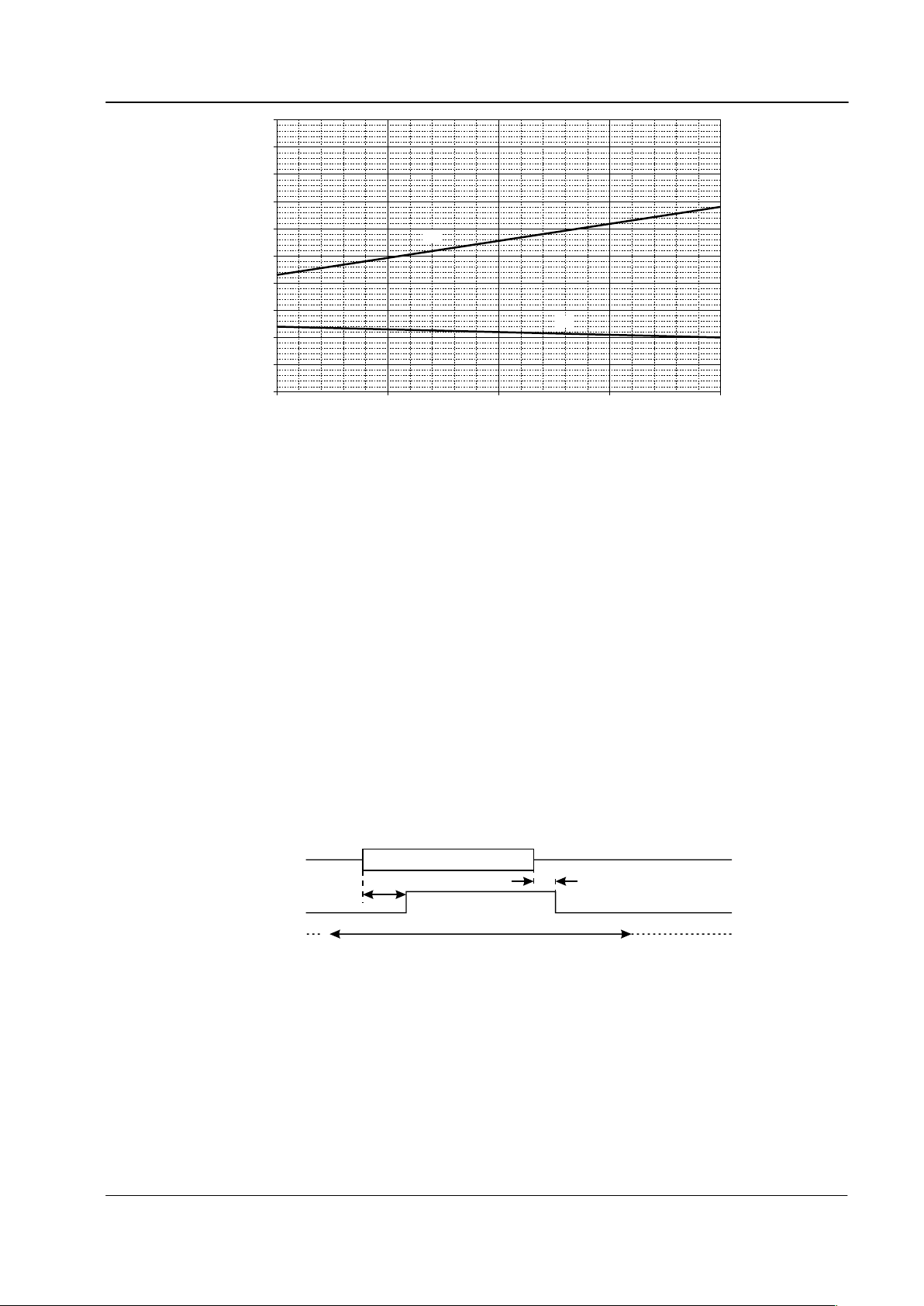
DET
Line Signal
MODE 1
MODE 2
FSK Receiver mode
FSK signal
t
EON
t
EOFF
See Section 6.1 for definitions of t
EON
and t
EOFF
Figure 6: FSK Level Detector Operation
4.5 FSK Demodulator
This FSK Demodulator block converts the 1200 baud FSK input signal to a logic level received data signal
which is output via the RXD pin as long as the Data Retiming function is not enabled (see Section 4.6). This
output does not depend on the state of the FSK Level Detector output.
N
ote:
In the absence of a valid FSK signal, the demodulator may falsely interpret speech or other extraneous
signals as data.
 Loading...