

MX COM Inc MX604DW, MX604P, MX604TN Datasheet
DATA BULLETIN
MX604
v.23 Compatible Modem
1998 MXCOM, INC. Tele: 800 638 5577 336 744 5050 Fax: 336 744 5054 Doc. # 20480152.004
4800 Bethania Station Road, Winston-Salem, NC 27105-1201 USA All trademarks and service marks are held by their respective companies.
PRELIMINARY INFORMATION
FEATURES APPLICATIONS
1200bps forward, 75bps back channels
Conforms to relevant sections of v.23
and ETSI specifications
Line Equalization
1200bps Data Retiming Facility can
eliminate external UART
Low Voltage Operation (3.3 to 5.0V)
Low Power Operation
1mA typ. @ 3.3V Operating Mode
1A typ. Zero-Power Mode
Standard 3.58Mhz Xtal/Clock
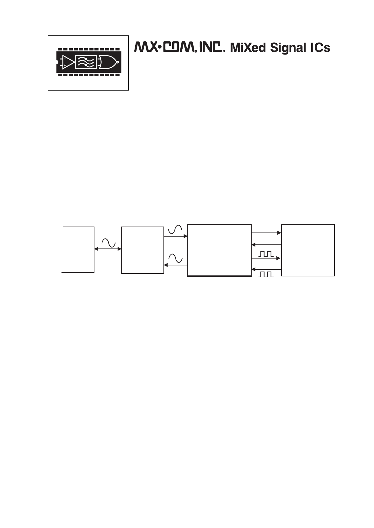
Telephone Telemetry System
Applications
µC
Data
Control
Status
MX604
Line
Interfa c e
Telephone
Line
The MX604 is a low voltage, low power CMOS device, used for the reception or transmission of asynchronous
1200bps data and full-duplex 75bps back channel data in accordance with CCITT V.23 and ETSI
specifications.
This device provides an optional Tx and Rx data retiming function which can eliminate, based on user
preference, the need for an external UART when operating at 1200bps. The device can disable the back
channel or be operated so only the mark or space tone is produced. The optional line equalizer is
incorporated into the receive path and is controlled by an external logic level.
The MX604 may be used in a wide range of telephone telemetry systems. Low voltage capability, a low
operating current (1mA typ. @ V
DD
= 3.3V), and a very low current 'sleep' mode (1A typ.) make the MX604
ideal for both portable terminal and line powered applications.
The MX604 is available in the following packages: 24-pin TSSOP (MX604TN), 16-pin SOIC (MX604DW) and
16-pin PDIP (MX604P).

v.23 Compatible Modem 2 MX604 PRELIMINARY INFORMATION
1998 MXCOM, INC. Tele: 800 638 5577 336 744 5050 Fax: 336 744 5054 Doc. # 20480152.004
4800 Bethania Station Road, Winston-Salem, NC 27105-1201 USA All trademarks and service marks are held by their respective companies.
CONTENTS
Section Page
1. Block Diagram ..........................................................................................................3
2. Signal List .................................................................................................................4
3. External Components ..............................................................................................5
4. General Description .................................................................................................5
4.1 Xtal Osc and Clock Dividers................................................................................................... 5
4.2 Mode Control Logic ................................................................................................................ 6
4.3 Rx Input Amplifier................................................................................................................... 6
4.4 Receive Filter and Equalizer................................................................................................... 6
4.5 Energy Detector...................................................................................................................... 7
4.6 FSK Demodulator................................................................................................................... 7
4.7 FSK Modulator and Transmit Filter......................................................................................... 7
4.8 Rx Data Retiming ................................................................................................................... 9
4.9 Tx Data Retiming.................................................................................................................. 10
5. Application..............................................................................................................11
5.1 Line Interface........................................................................................................................ 11
6. Performance Specification....................................................................................12
6.1 Electrical Performance ......................................................................................................... 12
6.2 Timing................................................................................................................................... 15
6.3 Packaging............................................................................................................................. 16
MXCOM, Inc. reserves the right to change specifications at any time and without notice
v.23 Compatible Modem 3 MX604 PRELIMINARY INFORMATION
1998 MXCOM, INC. Tele: 800 638 5577 336 744 5050 Fax: 336 744 5054 Doc. # 20480152.004
4800 Bethania Station Road, Winston-Salem, NC 27105-1201 USA All trademarks and service marks are held by their respective companies.
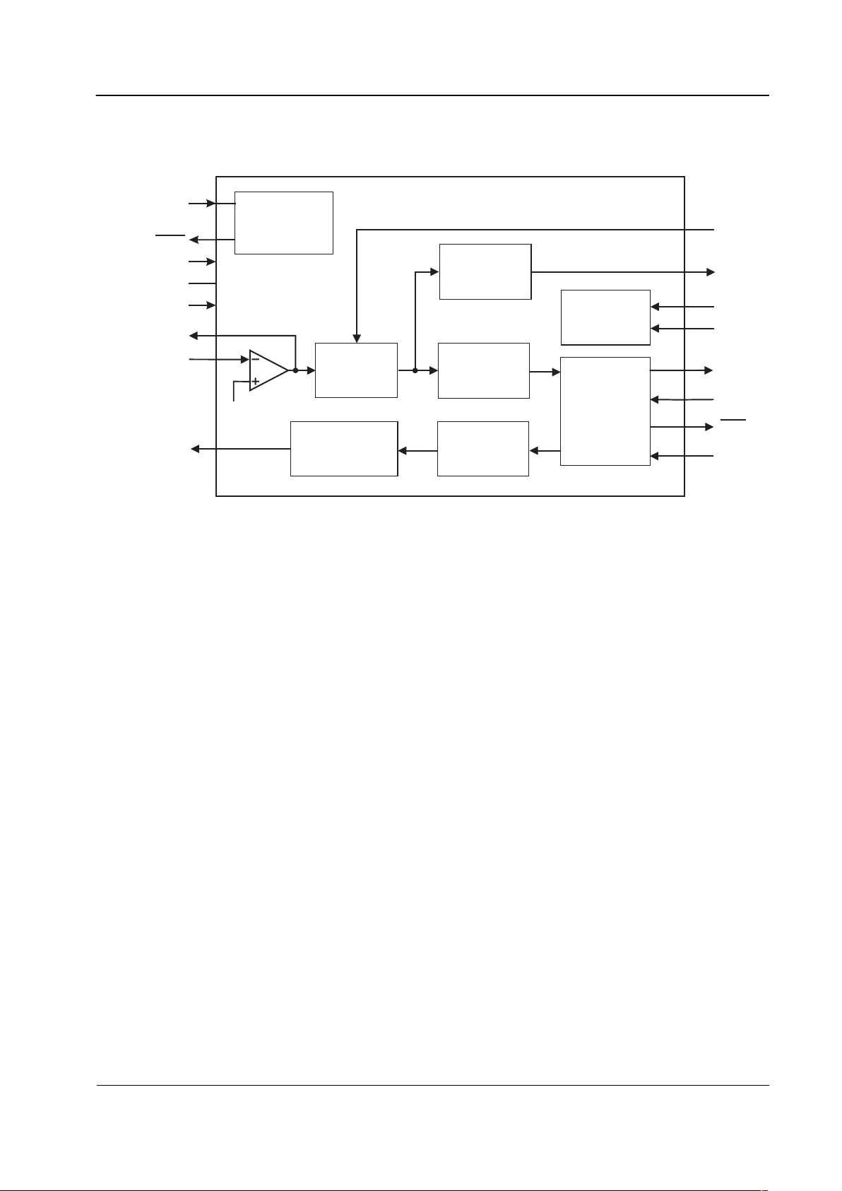
1. Block Diagram
TXD
M0
RXEQ
CLK
RXD
RD Y
M1
DET
Energy
Detect
FSK
De-modulator
Receive
Filter and
Equalizer
Mode
Control
Logic
Rx/Tx Data
Re-timing
Transmit Filter
and Output Buffer
FSK
Modulator
RXIN
RXAMPOUT
TXOUT
Xtal Osc and
Clock Dividers
XTAL/
CLOCK
XTAL
V
DD
V
BIAS
V
BIAS
V
SS
Figure 1: Block Diagram

v.23 Compatible Modem 4 MX604 PRELIMINARY INFORMATION
1998 MXCOM, INC. Tele: 800 638 5577 336 744 5050 Fax: 336 744 5054 Doc. # 20480152.004
4800 Bethania Station Road, Winston-Salem, NC 27105-1201 USA All trademarks and service marks are held by their respective companies.
2. Signal List
Pin No. Name Type Description
P, DW
TN
1
1
XTAL
output Output of the on-chip Xtal oscillator inverter.
2
2
XTAL/CLOCK input Input to the on-chip Xtal oscillator inverter.
3
5
M0 input A logic level input for setting the mode of the device.
See section 4.2
4
6
M1 input A logic level input for setting the mode of the device.
See section 4.2
5
7
RXIN input Input to the Rx input amplifier.
6
8
RXAMPOUT output Output of the Rx input amplifier.
7
11
TXOUT output Output of the FSK generator.
8
12
V
SS
power Negative supply (ground).
9
13
V
BIAS
output Internally generated bias voltage, held at VDD /2
when the device is not in 'Zero-Power' mode.
Should be decoupled to V
SS
by a capacitor
mounted close to the device pins.
10
14
RXEQ input A logic level input for enabling/disabling the
equalizer in the receive filter. See section 4.4
11
17
TXD input A logic level input for either the raw input to the FSK
Modulator or data to be re-timed depending on the
state of the M0, M1 and CLK inputs.
See section 4.9
12
18
CLK input A logic level input which may be used to clock data
bits in/out of the FSK Data Retiming block.
13
19
RXD output A logic level output carrying either the raw output of
the FSK Demodulator or re-timed characters
depending on the state of the M0, M1 and CLK
inputs. See section 4.8
14
20
DET output A logic level output of the on-chip energy detect
circuit.
15
23
RDY
output "Ready for data transfer" output of the on-chip data
retiming circuit. This open-drain active low output
may be used as an Interrupt Request/Wake-up
input to the associated C. An external pull-up
resistor should be connected between this output
and V
DD
.
16
24
V
DD
power The positive supply rail. Levels and thresholds
within the device are proportional to this voltage.
Should be decoupled to V
SS
by a capacitor
mounted close to the device pins.
3, 4, 9, 10 ,15,
16, 21, 22
N/C No internal connections
This device is capable of detecting and decoding small amplitude signals. Achieving the VDD and V
BIAS
decoupling and protection of the receive path from extraneous in-band signals is very important. It is
recommended that decoupling capacitors be placed so the connection between them and the device pins is
as short as possible. A ground plane protecting the receive path will help attenuate interfering signals.
v.23 Compatible Modem 5 MX604 PRELIMINARY INFORMATION
1998 MXCOM, INC. Tele: 800 638 5577 336 744 5050 Fax: 336 744 5054 Doc. # 20480152.004
4800 Bethania Station Road, Winston-Salem, NC 27105-1201 USA All trademarks and service marks are held by their respective companies.
3. External Components
V
DD
V
BIAS
V
SS
MX604
16
15
14
13
12
11
10
98
7
6
5
4
3
2
1
DET
RDY
CLK
RXEQ
RXD
TXD
M1
TXOUT
RXAMPOUT
RXIN
M0
To/From µC
From µC
C1
C2
C3
C4
X1
R1
XTAL/CLOCK
XTAL
V
DD
R1
100k
5%,
C1, C2 18pF
10%
C3
0.1F
10%
C4
0.1F
10%
X1 Note 1 3.579545MHz
Figure 2: Recommended External Components for Typical Application
External Components Notes:
1. A crystal frequency of 3.579545MHz 0.1% is required for correct FSK operation. For best results, a
crystal oscillator design should drive the clock inverter input with signal levels of at least 40% of V
DD
,
peak-peak. Tuning fork crystals generally cannot meet this requirement. To obtain crystal oscillator
design assistance, consult your crystal manufacturer. Operation of this device without a Xtal or Clock
input may cause device damage.
4. General Description
4.1 Xtal Osc and Clock Dividers
Frequency and timing accuracy of the MX604 is determined by a 3.579545MHz clock present at the
XTAL/CLOCK pin. This may be generated by the on-chip oscillator inverter using the external components
C1, C2 and X1 of Figure 2, or it may be supplied from an external source to the XTAL/CLOCK input. If
supplied from an external source, C1, C2 and X1 should not be used.
The on-chip oscillator is disabled in the 'Zero-Power' mode.
If the clock is provided by an external source which is not always running, then the 'Zero-Power' mode must
be set when the clock is not available. Failure to observe this rule may cause a significant rise in the supply
current drawn by MX604 as well as generating undefined states of the RXD, DET and
RDY outputs.
v.23 Compatible Modem 6 MX604 PRELIMINARY INFORMATION
1998 MXCOM, INC. Tele: 800 638 5577 336 744 5050 Fax: 336 744 5054 Doc. # 20480152.004
4800 Bethania Station Road, Winston-Salem, NC 27105-1201 USA All trademarks and service marks are held by their respective companies.
4.2 Mode Control Logic
The MX604's operating mode is determined by the logic levels applied to the M0 and M1 input pins:
M1 M0 Rx Mode Tx Mode
Data Retime
[1]
0 0 1200bps 75bps Rx
0 1 off 1200bps Tx
1 0 1200bps off Rx
1 1 'Zero-Power' -
[1] If enabled.
Note: On applying power to the device the mode must be set to 'ZP', i.e. M0=1, M1=1, until V
DD
has
stabilized.
In the 'Zero-Power' mode, power is removed from all internal circuitry. When leaving 'Zero-Power' mode there
must be a 20ms delay before any Tx data is passed to, or Rx data read from, the device to allow the bias
level, filters and oscillator to stabilize.
4.3 Rx Input Amplifier
The Rx Input Amplifier is used to adjust the signal received to the correct amplitude for the FSK receiver and
Energy Detect circuits (see section 5.1).
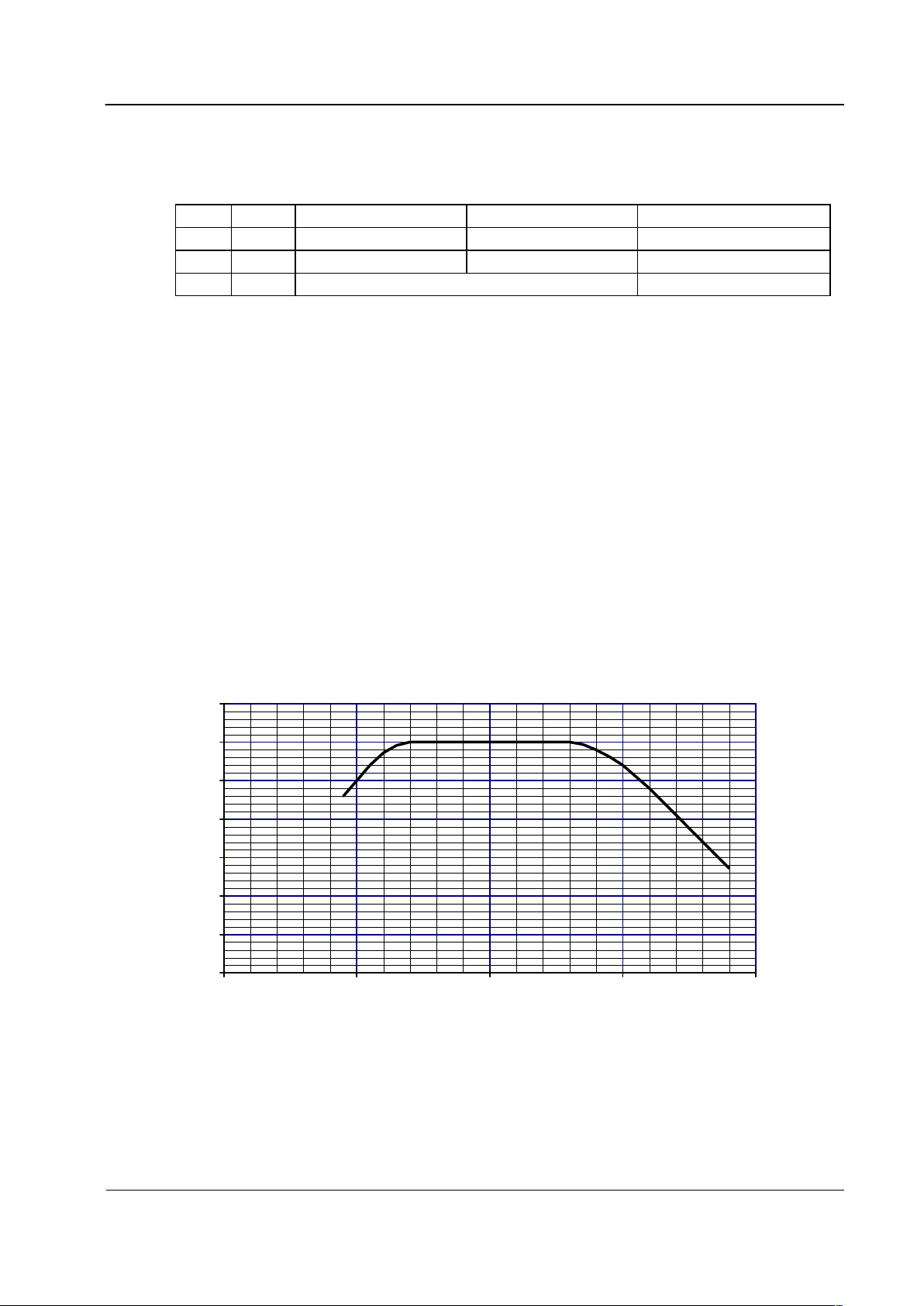
4.4 Receive Filter and Equalizer
The Receive Filter and Equalizer is used to attenuate out of band noise and interfering signals, especially the
locally generated 75bps transmit tones which might otherwise reach the 1200bps FSK Demodulator and
Energy Detector circuits. This block also includes a switchable equalizer section. When the RXEQ pin is low
the overall group delay of the receive filter is flat over the 1200bps frequency range. If the RXEQ pin is high
the receive filter's typical overall group delay will be as shown in Figure 3.
-0.15
-0.125
-0.1
-0.075
-0.05
-0.025
0
0.025
500 1000 1500 2000 2500
Delay/ms
Frequency/Hz
Figure 3: Rx Equalizer Group Delay (RXEQ = 1) with respect to 1700Hz
 Loading...