

MX COM Inc MX589DW, MX589P Datasheet
DATA BULLETIN
MX589
High Speed GMSK Modem
1998 MX-COM, Inc. www.mxcom.com Tele: 800 638 5577 336 744 5050 Fax: 336 744 5054 Doc. # 20480103.010
4800 Bethania Station Road, Winston-Salem, NC 27105-1201 USA All trademarks and service marks are held by their respective companies.
Features Applications
•
Data Rates from 4kbps to 64kbps
•
Full or Half Duplex Gaussian Minimum Shift
Keying (GMSK) Operation
•
Selectable BT: (0.3 or 0.5)
•
Low Power
3.0V, 20kbps, 1.5mA typ.
5.0V, 64kbps, 4.0mA typ.
•
Low Current Non-DSP Solution
•
Small TSSOP size fits PCMCIA / PC CARDs
•
Point of Sale Terminals
•
Low Power Wireless Data Link for
PCs, Laptops, and Printers
•
Data for GPS/Differential GPS
•
Portable Wireless Data Applications
Cellular Digital Packet Data (CDPD)
Mobitex Mobile Data System
TX PS
RX PS
BT
TX D ATA
ClkDIVA
PLLacq
RXDCacq
RX SIGNAL IN
RX FEEDBACK
CLOCK
DIVIDER
XTAL/CLOCK
TX ENABLE
XTAL
V
DD
V
BIAS
V
BIAS
V
BIAS
V
SS
RXHold
RX CLK
TX CLK
TX OUT
RX DAT A
RX S/N
DOC1 DOC2
ClkDIVB
RX CIRCUIT
CONTROL
RX
FILTER
DA TA RETIME &
LEVEL SHIFT
TX
FILTER
RX S/N
DETECTION
RX CLOCK
RX DC LEVEL
MEASURE
+
-
V
BIAS
RX DATA
DETECTION
The MX589 is a single-chip synchronous modem designed for Wireless Data Applications. Employing Gaussian Minimum
shift Keying (GMSK) baseband modulation, the MX589 features a wide range of available data rates: 4k to 64kbps. Data
Rates and the choice of BT (0.3 or 0.5) are pin programmable to provide for different system requirements.
The Tx and Rx digital data interfaces are bit serial, synchronized to Tx and Rx data clocks generated by the modem.
Separate Tx and Rx Powersave inputs allow full or half-duplex operation. Rx input levels can be set by suitable AC and
DC level adjusting circuitry built with external components around an on-chip Rx Input Amplifier.
Acquisition, Lock, and Hold of Rx data signals are made easier and faster by the use of Rx Control Inputs to clamp,
detect, and /or hold input data levels and can be set by the µProcessor as required. The Rx S/N output provides an
indication of the quality of the received signal.
The MX589 may be used with a 3.0V to 5.5V power supply and is available in the following packages: 24-pin TSSOP
(MX589TN), 24-pin SOIC (MX589DW), and 24-pin PDIP (MX589P).

High Speed GMSK Modem 4k to 64kbps 2 MX589
1998 MX-COM, Inc. www.mxcom.com Tele: 800 638 5577 336 744 5050 Fax: 336 744 5054 Doc. # 20480103.010
4800 Bethania Station Road, Winston-Salem, NC 27105-1201 USA All trademarks and service marks are held by their respective companies.
Contents
Section Page
1 Block Diagram................................................................................................................................. 3
2 Signal List ....................................................................................................................................... 4
3 External Components..................................................................................................................... 5
4 General Description........................................................................................................................ 7
4.1 Clock Oscillator Divider .......................................................................................................................... 7
4.2 Receive .................................................................................................................................................. 7
4.2.1 Rx Signal Path Description..........................................................................................................................7
4.2.2 Rx Circuit Control Modes ............................................................................................................................8
4.2.3 Rx Clock Extraction.....................................................................................................................................9
4.2.4 Rx Data Extraction ......................................................................................................................................9
4.2.5 Rx S/N Detection.........................................................................................................................................9
4.2.6 Rx Signal Quality........................................................................................................................................10
4.3 Transmit ................................................................................................................................................ 11
4.3.1 TX Signal Path Description ........................................................................................................................11
4.4 Data Formats......................................................................................................................................... 13
4.5 Acquisition and Hold Modes.................................................................................................................. 13
5 Application..................................................................................................................................... 14
5.1 Radio Channel Requirements ............................................................................................................... 14
5.1.1 Bit Rate, BT, and Bandwidth......................................................................................................................14
5.1.2 FM Modulator, Demodulator and IF ...........................................................................................................14
5.1.3 Two-Point Modulation.................................................................................................................................15
5.2 AC Coupling of Tx and Rx Signals........................................................................................................ 16
6 Performance Specifications ......................................................................................................... 17
6.1 Electrical Specifications......................................................................................................................... 17
6.1.1 Absolute Maximum Limits ..........................................................................................................................17
6.1.2 Operating Limits.........................................................................................................................................17
6.1.3 Operating Characteristics...........................................................................................................................18
6.1.4 Packages....................................................................................................................................................19
MXCOM, Inc. reserves the right to change specifications at any time without notice.
High Speed GMSK Modem 4k to 64kbps 3 MX589
1998 MX-COM, Inc. www.mxcom.com Tele: 800 638 5577 336 744 5050 Fax: 336 744 5054 Doc. # 20480103.010
4800 Bethania Station Road, Winston-Salem, NC 27105-1201 USA All trademarks and service marks are held by their respective companies.
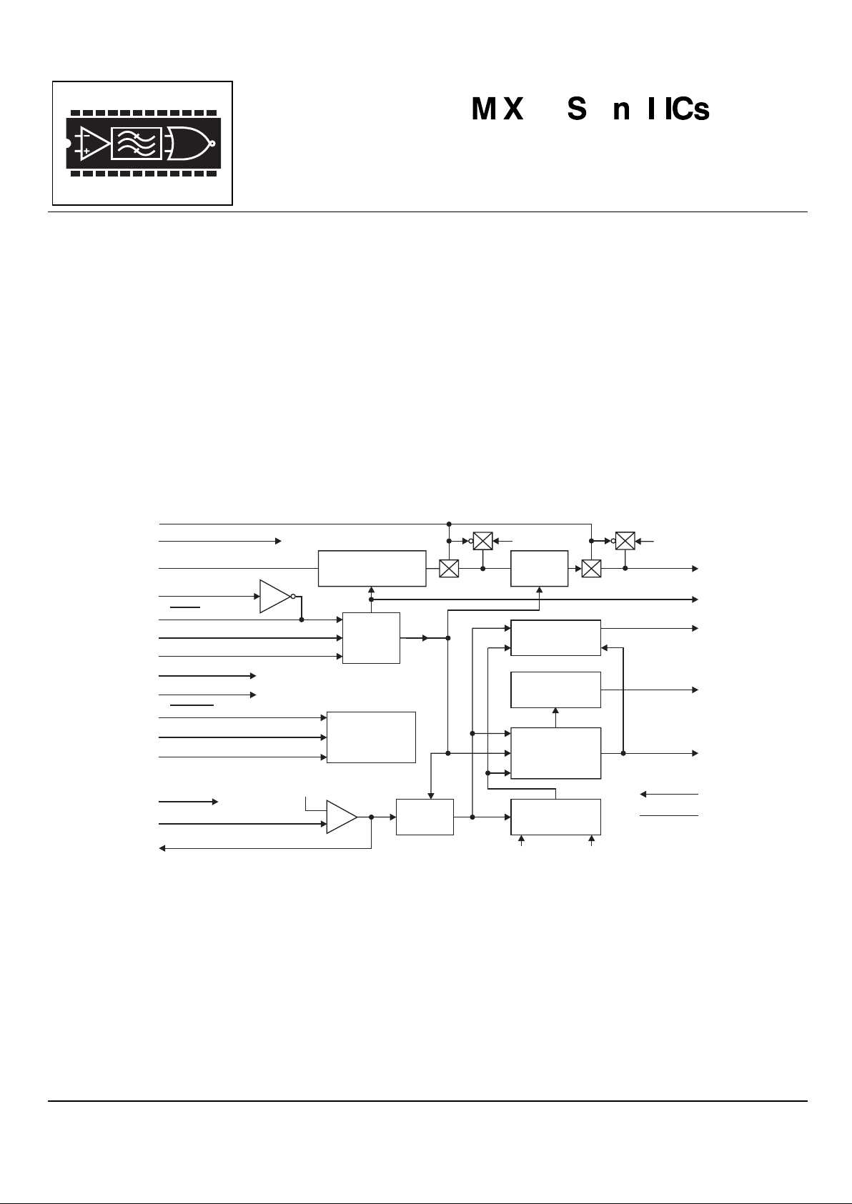
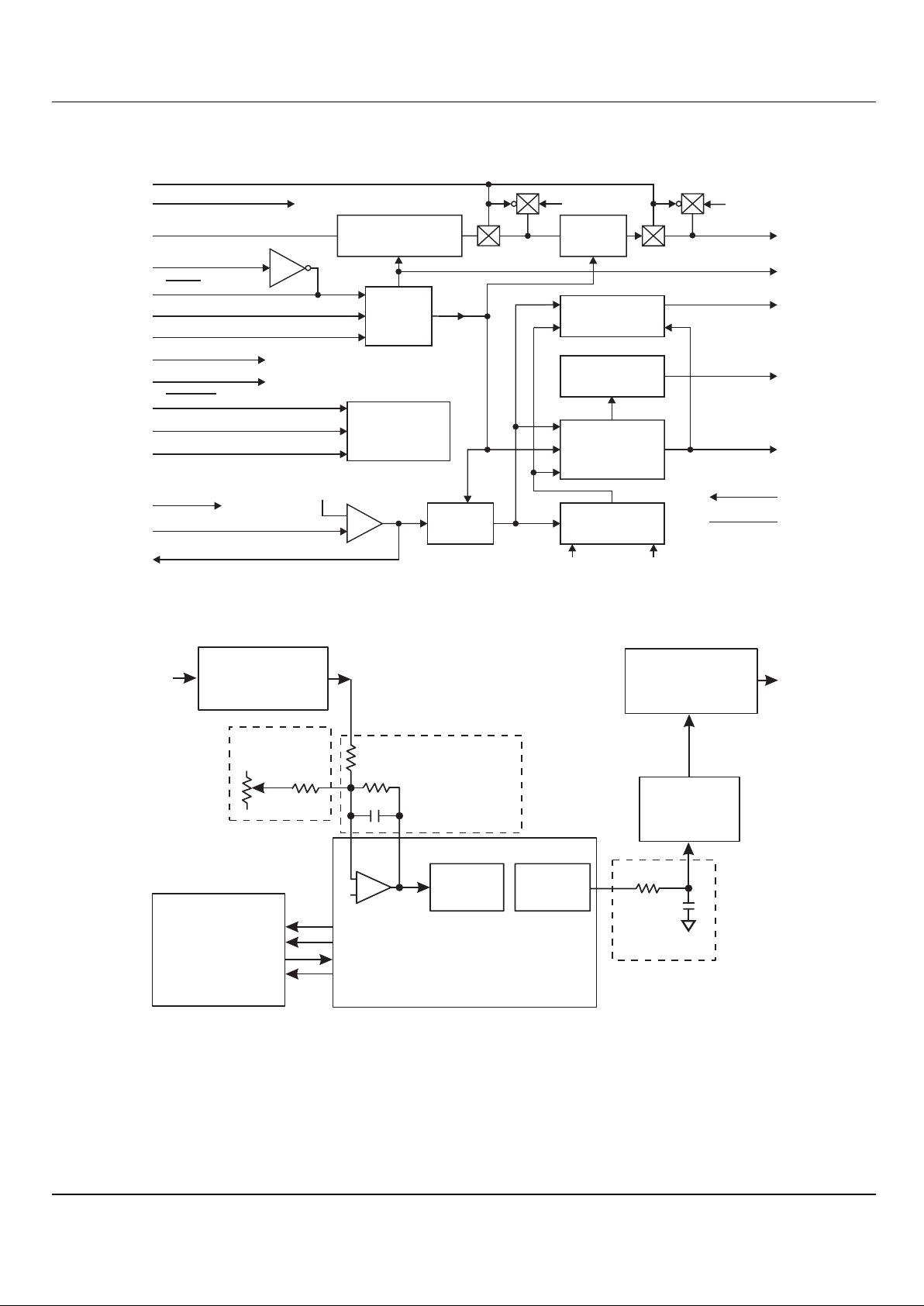
1 Block Diagram
TX PS
RX PS
BT
TX DATA
ClkDIVA
PLLacq
RXDCacq
RX SIGNAL IN
RX FEEDBACK
CLOCK
DIVIDER
XTAL/CLOCK
TX ENABLE
XTAL
V
DD
V
BIAS
V
BIAS
V
BIAS
V
SS
RXHold
RX CLK
TX CLK
TX OUT
RX DAT A
RX S/N
DOC1 DOC2
ClkDIVB
RX CIRCUIT
CONTROL
RX
FILTER
DA TA RETIME &
LEVEL SHIFT
TX
FILTER
RX S/N
DETECTION
RX CLOCK
RX DC LEVEL
MEASURE
+
-
V
BIAS
RX DATA
DETECTION
Figure 1: Block Diagram
RX Frequency
Discriminator
Frequency
Modulator
Signal and
DC Level
Adjustment
DC Level
Adjust
RX Sig In
RX Feedback
RX circuits
TX circuits
RXD
RXC
TXD
TXC
uController
or UAR T
RX Data
RX Clock
TX Data
TX Clock
MX589
GMSK MODEM
TX Out
TX Out
Filter
RX Filter
and Gain
Figure 2: System Block Diagram

High Speed GMSK Modem 4k to 64kbps 4 MX589
1998 MX-COM, Inc. www.mxcom.com Tele: 800 638 5577 336 744 5050 Fax: 336 744 5054 Doc. # 20480103.010
4800 Bethania Station Road, Winston-Salem, NC 27105-1201 USA All trademarks and service marks are held by their respective companies.
2 Signal List
Pin No.
TN/DW/P
Signal Type Description
1
XTAL
output The output of the on-chip clock oscillator.
2 XTAL/CLOCK input
The input to the on-chip Xtal oscillator. A Xtal, or externally derived clock (f
XTAL
)
pulse input should be connected here. If an externally generated clock is to be
used, it should be connected to this pin and the
XTALpin left unconnected.
Note: Operation of the MX589 without a suitable Xtal or clock input may cause
device damage.
3 ClkDivA input Logic level inputs control the internal clock divider and therefore the transmit and
receive data rate. See Table 4.
4 ClkDivB input
Logic level inputs control the internal clock divider and therefore the transmit and
receive data rate. See Table 4.
5
HOLDRx
input
A logic 0 applied to this input will freeze the Clock Extraction and Level
Measurement circuits unless they are in ‘Acquire’ mode.
6 RxDCacq input A logic 1 applied to this input will set the RX Level Measurement circuitry to the
Acquire mode.
7 PLLacq input A logic 1 applied to this input will set the RX Clock Extraction circuitry to the
‘Acquire’ mode. See Table 5.
8 Rx PSAVE input A logic 1 applied to this input will powersave all receive circuits except for RX
CLK output (which will continue at the set bit-rate) and cause the RX Data and
RX S/N outputs to go to a logic 0.
9
V
BIAS
The internal circuitry bias line, held at VDD/2. This pin must be bypassed to V
SS
by a capacitor mounted close to the pin.
10 Rx FB Output of the RX Input Amplifier.
11 Rx Signal In input Input to RX input amplifier.
12
V
SS
power Negative supply (GND).
13 DOC1 Connections to the RX Level Measurement Circuitry. A capacitor should be
connected from each pin to V
SS
.
14 DOC2
Connections to the RX Level Measurement Circuitry. A capacitor should be
connected from each pin to V
SS
.
15 BT A logic level to select the modem BT (the ratio of the TX Filter's -3dB frequency
to the Bit-Rate). A logic 1 = BT of 0.5 and a logic 0 = BT of 0.3.
16 Tx Out output The TX signal output from the MX589 GMSK Modem.
17 Tx Enable input A logic 1 applied to this input, enables the transmit data path, through the TX
Filter to the TX Out pin. A logic 0 will place the TX Out pin to V
BIAS
via a high
impedance.
18 Tx PSAVE input
A logic 1 applied to this input will powersave all transmit circuits except for the
TX Clock.
19 Tx Data input The logic level input for the data to be transmitted. This data should be
synchronous with TX CLK.
20 Rx Data output A logic level output carrying the received data, synchronous with RX CLK.
21 Rx CLK output A logic level clock output at the received data bit-rate.
22 Tx CLK output A logic level clock output at the transmit-data rate.
23 Rx S/N output A logic level output which may be used as an indication of the quality of the
received signal.
24
V
DD
power Positive supply. A single 5.0V power supply is required. Levels and voltages
within this modem are dependent upon this supply. This pin should be bypassed
to V
SS
by a capacitor mounted close to the pin.
High Speed GMSK Modem 4k to 64kbps 5 MX589
1998 MX-COM, Inc. www.mxcom.com Tele: 800 638 5577 336 744 5050 Fax: 336 744 5054 Doc. # 20480103.010
4800 Bethania Station Road, Winston-Salem, NC 27105-1201 USA All trademarks and service marks are held by their respective companies.
Table 1: Signal List
3 External Components
ClkDivA
ClkDivB
RX HOLD
RXDCacq
PLLacq
RX PSAVE
V
BIAS
RX FB
RX SIGNAL IN
V
SS
V
DD
RX S/N
TXCLK
RXCLK
RXDATA
TXDATA
TXPSAVE
TXENABLE
TXOUT
BT
DOC1
DOC2
1
2
3
4
5
6
7
8
9
10
11
12
24
23
22
21
20
19
18
17
16
15
14
13
MX589
C6
R4
R3
C7 C8
C4
R1
C1
V
DD
XTAL/CLOCK
XTAL
XTAL
XTAL/CLOCK
1
2
C3
C2
X1 R2
C5
Figure 3: Recommended External Components
Component Notes Value Tolerance Component Notes Value Tolerance
R1 Note 1 ±5% C4 0.1µF ±20%
R2
1.0M
Ω
±10% C5 1.0µF ±20%
R3 Note 2 ±10% C6 22.0pF ±20%
R4
100k
Ω
±10% C7 Note 4
C1 Note 1 ±10% C8 Note 4
C2 Note 3
C3 Note 3 X1 Note 5
Table 2: Recommended External Components
High Speed GMSK Modem 4k to 64kbps 6 MX589
1998 MX-COM, Inc. www.mxcom.com Tele: 800 638 5577 336 744 5050 Fax: 336 744 5054 Doc. # 20480103.010
4800 Bethania Station Road, Winston-Salem, NC 27105-1201 USA All trademarks and service marks are held by their respective companies.
Recommended External Component Notes:
1.
The RC network formed by R1 and C1 is required between the TX Out pin and the input to the modulator. This
network, which can form part of any DC level shifting and gain adjustment circuitry, forms an important part of the
transmit signal filtering. The ground connection to the capacitor C1 should be positioned to give maximum attenuation
of high-frequency noise into the modulator.
The component values should be chosen so that the product of the resistance and the capacitance is:
For a BT of 0.3 R1C1 = 0.34/bit rate (bps)
For a BT of 0.5 R1C1 = 0.22/bit rate (bps)
BT =- 0.3 BT = 0.5
Data Rates
(bps)
R1 C1 R1 C1
4000
120k
Ω
680pF
120k
Ω
470pF
4800
100k
Ω
680pF
100k
Ω
470pF
8000
91k
Ω
470pF
120k
Ω
220pF
9600
91k
Ω
390pF
47k
Ω
470pF
16000
47k
Ω
470pF
91k
Ω
150pF
19200
100k
Ω
180pF
91k
Ω
120pF
32,000
47k
Ω
220pF
47k
Ω
150pF
38,400 *
47k
Ω
180pF
47k
Ω
120pF
64,000 *
56k
Ω
100pF
51k
Ω
68pF
* VDD ≥ 4.5V
Table 3: Data Rate vs. BT and Selected External Component Values
Note: In all cases, the value of R1 should not be less than 20.0kΩ, and that the calculated value of C1 includes
calculated parasitic capacitance.
2. R3, R4 and C6 form the gain components for the RX Input signal. R3 should be chosen as required by the signal
input level.
3. The values chosen for C2 and C3 (including stray capacitance), should be suitable for the applied VDD and the
frequency of X1.
As a guide: C2 = C3 = 33pF at 1.0MHz falling to 18pF at the maximum frequency.
At 3.0V, C2 = C3 = 33pF falling to 18pF at 5.0MHz the equivalent series resistance of X1 should be less than 2.0K
Ω
falling to 150Ω at the maximum frequency. Stray capacitance on the Xtal/Clock circuit pins must be minimized.
4. C7 and C8 should both be .015µF for a data rate of 8kbps, and inversely proportional to the data rate for other data
rates, e.g. .030µF at 4kbps, 1800pF at 64kbps.
5. The MX589 can operate correctly with the Xtal/Clock frequencies between 1.0MHz and 8.2MHz (V
DD
= 5.0V) and
1.0MHz to 5.0MHz (V
DD
= 3.0V) see Table 1 for examples. For best results, a crystal oscillator design should drive
the clock inverter input with signal levels of at least 40% of VDD, peak to peak. Tuning fork crystals generally cannot
meet this requirement. To obtain crystal oscillator design assistance, consult your crystal manufacturer. Operation of
this device without a Xtal or Clock input may cause device damage.
 Loading...