DATA BULLETIN
MX469
1200/2400/4800bps MSK Modem
1998 MX-COM, Inc. www.mxcom.com Tel: 800 638 5577 336 744 5050 Fax: 336 744 5054 Doc. # 20480081.010
4800 Bethania Station Road, Winston-Salem, NC 27105-1201 USA All trademarks and service marks are held by their respective companies.
Features Applications
Selectable Data Rates
1200/2400/4800bps
Full-Duplex MSK
RX and TX Bandpass Filters
Clock Recovery and
Carrier Detect Capabilities
Pin Selected Xtal/Clock Inputs
1.008MHz or 4.032MHz
Radio and General Applications
Data-Over-Radio
PMR/Cellular Signaling
Portable Data Terminals
Personal/Cordless Telephone
CLOCK
OSCILLA TOR
DIVIDER
DAT A
LA TCH
DIGITAL
PLL
RECTIFIER
S/N
COMP ARATOR
NOISE FILTER
RECTIFIER
RX FILTER
RX ENABLE
DAT A
FILTER
DIGITAL
FILTER
LIMITER LIMITER
RETRIGGERABLE
MONOST ABLE
TX GENERATOR
XT AL/CLOCK
CLOCK RATE
TX DATA I/P
RX SIGNAL I/P
TX SIGNAL O/P
UNCLOCKED
DAT A O/P
CLOCKED
DAT A O/P
RX SYNC O/P
BANDP ASS O/P
CARRIER DETECT O/P
CARRIER DETECT TIME CONST ANT
TX SYNC O/P
TX FILTER
XT AL
f
.. n
V
DD
V
SS
V
BIAS
4800 BPS SELECT
TX ENABLE
1200/ BPS SELECT2400
The MX469 is a full-duplex pin-selectable 1200/2400/4800bps Minimum Shift Key (MSK) Modem for FM radio
links. The mark and space frequencies are 1200/1800, 1200/2400, and 2400/4800Hz respectively. Tone
frequencies are phase continuous; transitions occur at the zero crossing point. The use of a common Xtal
oscillator with a choice of two clock frequencies (1.008MHz or 4.032MHz) provides data-rate, transmit
frequencies, and RX/TX synchronization. The transmitter and receiver operate entirely independently
including individual section powersave functions.
The MX469 includes on-chip circuitry for Carrier Detect and RX Clock Recovery, both of which are made
available at output pins. RX, TX, and Carrier Detect circuits contain bandpass filters to provide high quality
signals in their respective paths. The carrier detect time constant is set by an external capacitor, whose value
should be arranged as required to further enhance this product's performance in high-noise environments.
The MX469 demonstrates high sensitivity and good bit-error-rate under adverse signal conditions.
This low-power device requires few external components and is available in the following packages:
24-pin SOIC (MX469DW), 22-pin PDIP (MX469P), and 20-pin SOIC (MX469D3).

1200/2400/4800bps MSK Modem 2 MX469
1998 MX-COM, Inc. www.mxcom.com Tel: 800 638 5577 336 744 5050 Fax: 336 744 5054 Doc. # 20480081.010
4800 Bethania Station Road, Winston-Salem, NC 27105-1201 USA All trademarks and service marks are held by their respective companies.
Contents
Section Page
1. Block Diagram................................................................................................................3
2. Signal List.......................................................................................................................4
3. External Components....................................................................................................6
4. General Description.......................................................................................................7
4.1 Timing.................................................................................................................................. 7
4.1.1 1200bps ..................................................................................................................................7
4.1.2 2400bps ..................................................................................................................................8
4.1.3 4800bps ..................................................................................................................................9
5. Application ...................................................................................................................10
5.1 Synchronous Modem Design Considerations ................................................................... 10
5.2 Bit Error Rate..................................................................................................................... 11
6. Performance Specifications........................................................................................12
6.1 Electrical Specifications..................................................................................................... 12
6.1.1 Absolute Maximum Limits.....................................................................................................12
6.1.2 Operating Limits....................................................................................................................12
6.1.3 Operating Characteristics......................................................................................................13
6.1.4 Packages ..............................................................................................................................15
MXCOM, Inc. reserves the right to change specifications at any time and without notice.

1200/2400/4800bps MSK Modem 3 MX469
1998 MX-COM, Inc. www.mxcom.com Tel: 800 638 5577 336 744 5050 Fax: 336 744 5054 Doc. # 20480081.010
4800 Bethania Station Road, Winston-Salem, NC 27105-1201 USA All trademarks and service marks are held by their respective companies.
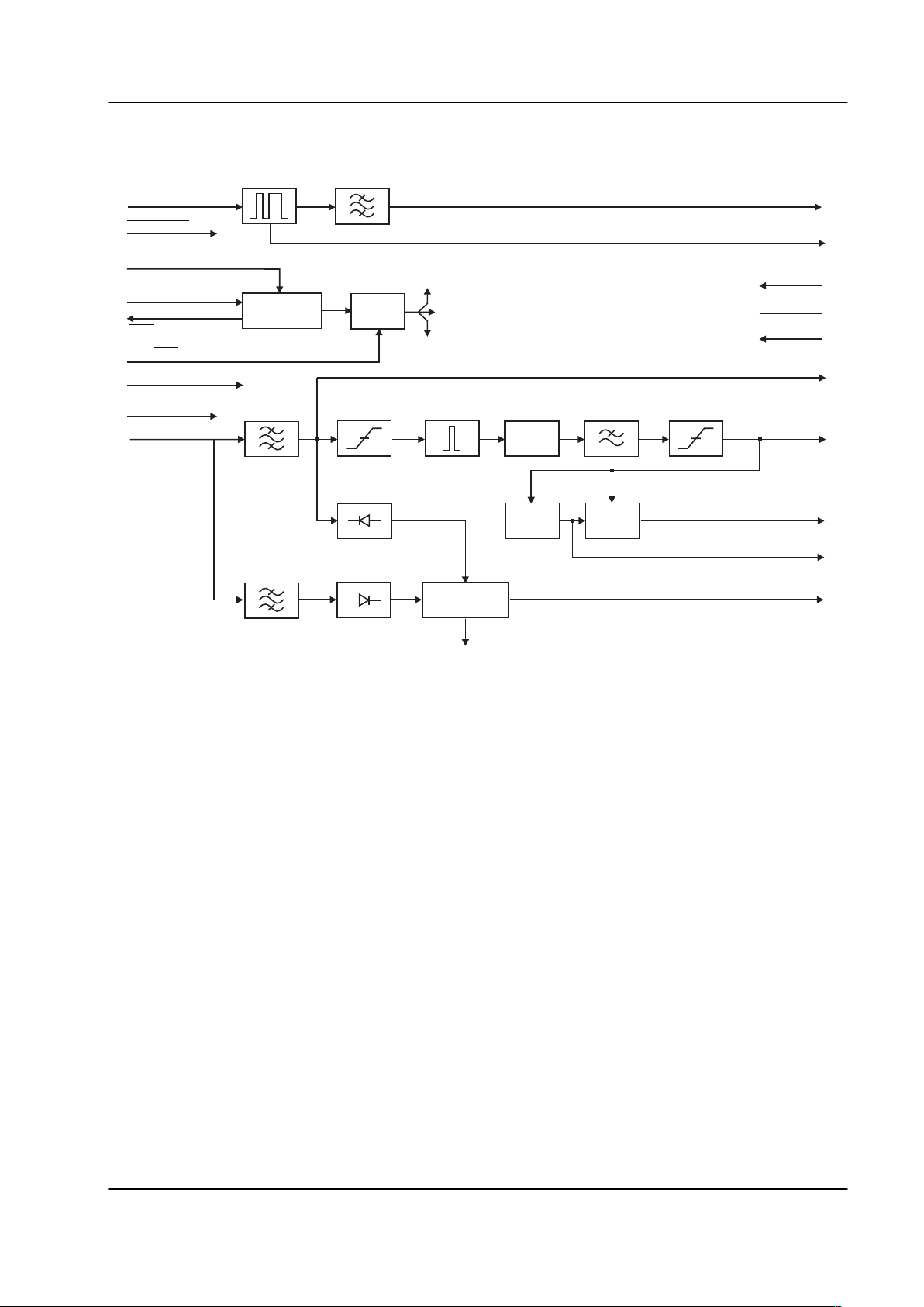
1. Block Diagram
CLOCK
OSCILLATOR
DIVIDER
DATA
LATCH
DIGITAL
PLL
RECTIFIER
S/N
COMPARATOR
NOISE FILTER
RECTIFIER
RX FILTER
RX ENABLE
DATA
FILTER
DIGITAL
FILTER
LIMITER LIMITER
RETRIGGERABLE
MONOSTABLE
TX GENERATOR
XTAL/CLOCK
CLOCK RATE
TX DATA I/P
RX SIGNAL I/P
TX SIGNAL O/P
UNCLOCKED
DATA O/P
CLOCKED
DATA O/P
RX SYNC O/P
BANDPASS O/P
CARRIER DETECT O/P
CARRIER DETECT TIME CONSTANT
TX SYNC O/P
TX FILTER
XTAL
f
.. n
V
DD
V
SS
V
BIAS
4800 BPS SELECT
TX ENABLE
1200/ BPS SELECT2400
Figure 1: Block Diagram

1200/2400/4800bps MSK Modem 4 MX469
1998 MX-COM, Inc. www.mxcom.com Tel: 800 638 5577 336 744 5050 Fax: 336 744 5054 Doc. # 20480081.010
4800 Bethania Station Road, Winston-Salem, NC 27105-1201 USA All trademarks and service marks are held by their respective companies.
2. Signal List
Signal Type Description
PDWD3
1 1 1 Xtal/Clock input The input to the on-chip inverter, for use with either a
1.008MHz or a 4.032MHz Xtal or external clock. Clock
frequency selection is by the “Clock Rate” input pin. The
selection of this frequency will affect the operational Data
Rate of this device. Refer to Table 3. Operation of any
MX•COM IC without a Xtal or clock input may cause
device damage. To minimize damage in the event of a
Xtal/drive failure, it is recommended that a current
limiting device (resistor or fast-reaction fuse) be installed
on the power supply (V
DD
).
22 2
Xtal
output Output of the on-chip inverter.
3 3 3 TX Sync output A squarewave, produced on-chip, to synchronize the
input of logic data and transmission of the MSK signal
(See Figure 3).
5 5 4 TX Signal output When the transmitter is enabled, this pin outputs the
(140-step pseudo sinewave) MSK signal (See Figure 3).
With the transmitter disabled, this output is set to a high-
impedance state.
6 7 5 TX Data input Serial logic data to be transmitted is input to this pin.
78 6
EnableTX
Input A logic ‘0’ will enable the transmitter (See Figure 3). A
logic ‘1’ at this input will put the transmitter into
powersave while forcing “TX Sync Out” to a logic ‘1’ and
“TX Signal Out” to a high-impedance state. This pin is
internally pulled to V
DD
.
8 9 7 Bandpass output The output of the RX Bandpass Filter. This output
impedance is typically 10k and may require buffering
prior to use.
9 10 8 RX Enable Input The control of the RX function. The control of other
outputs is provided in Table 2
10 11 9 V
BIAS
power The output of the on-chip analog bias circuitry. Held
internally at V
DD
/2, this pin should be decoupled to V
SS
by a capacitor (C2). See Figure 2 and RX Enable notes.
This bias voltage is maintained under all powersave
conditions.
11 12 10 V
SS
power Negative supply (GND).
12 13 11 Unclocked Data output The recovered asynchronous serial data output from the
receiver.
13 14 12 Clocked Data output The recovered synchronous serial data output from the
receiver. Data is latched out by the recovered clock,
available at the “RX Sync O/P”. (See Figure 4 and
Figure 6).
14 15 13 Carrier Detect output For 1200 and 2400bps operation only. When an MSK
signal is being received this output is a logic ‘1’. The
Carrier Detect signal should be ignored during 4800bps
operation.
15 16 14 RX Signal input The MSK signal input for the receiver. This input should
be coupled via a capacitor, C3.

1200/2400/4800bps MSK Modem 5 MX469
1998 MX-COM, Inc. www.mxcom.com Tel: 800 638 5577 336 744 5050 Fax: 336 744 5054 Doc. # 20480081.010
4800 Bethania Station Road, Winston-Salem, NC 27105-1201 USA All trademarks and service marks are held by their respective companies.
Signal Type Description
PDWD3
17 18 15 RX Sync output A flywheel squarewave output. This clock will
synchronize to incoming RX MSK data. (See Figure 4
and Figure 6).
16 19 16
1200/
2400BPS
Select
input A logic ‘1’ on this pin selects the 1200bps option; tone
frequencies are one cycle of 1200Hz represents a logic
‘1’, one-and-a-half cycles of 1800Hz represents a logic
‘0’. A logic ‘0’ on this pin selects the 2400bps option;
tone frequencies are one-half cycle of 1200Hz represents
a logic ‘1’, one cycle of 2400Hz represents a logic ‘0’.
This pin has an internal 1M pull-up resistor.
Operational Data Rate Configurations are illustrated in
Table 3
18 20 17 4800 BPS Select input A logic '1' on this pin combined with a logic '0' on the
1200/2400 BPS Select pin will select the 4800 option
(1M pulldown resistor). Tone frequencies are: one-half
cycle of 2400Hz represents a logic '1', one cycle of
4800Hz represents a logic '0'. This state can only be
achieved using a 4.032MHz Xtal input. Operational Data
Rate Configurations are illustrated in Table 3
19 21 18 Clock Rate input A logic input to select and allow the use of either a
1.008MHz or 4.032MHz Xtal/clock. Logic ‘1’ =
4.032MHz, logic ‘0’ = 1.008MHz. This input has an
internal pulldown resistor (1.008MHz).
20 23 19 Carrier Detect
Time Constant
output Part of the carrier detect integration function. The value
of C4 connected to this pin will affect the carrier detect
response time and therefore the noise performance (See
Figure 2, Note 3).
22 24 20 V
DD
power Positive supply. A single 5-volt supply is required.
4,214, 6,
17,
22
N/C No Internal Connection.
Table 1: Signal List
RX Enable = RX Function Clock Data Output Carrier Detect Rx Sync Out
1 = Enabled Enable Enabled Enabled
0 = Powersave 0 0 1 or 0
Table 2: RX Enable Control Functions
XTAL/CLOCK Frequency 1.008MHz 4.032MHz
Clock Rate pin 00111
1200/2400 Select Pin 10100
4800 Select Pin 00001
Data Rate (bps) 1200 2400 1200 2400 4800
Table 3: Operational Data Rate Configuration
 Loading...