MX COM Inc MX375J, MX375LH, MX375LH8, MX375P Datasheet

DATA BULLETIN
MX375
© 1997 MX•COM Inc. www.mxcom.com Tele: 800 638-5577 910 744-5050 Fax: 910 744-5054 Doc. # 20480026.007
4800 Bethania Station Road, Winston-Salem, NC 27105-1201 USA All trademarks and service marks are held by their respective companies.
Pvt
SQUELCHTM CTCSS
Encoder/Decoder
Features Applications
•
PRIVATE/CLEAR CAPABILITY
•
ON-CHIP TX AUDIO PRE/DEEMPHASIS
•
ALTERNATIVE TO STANDARD CTCSS
“PARTY LINE”
•
POWERSAVE OPTION
•
MOBILE RADIOS
•
COMMUNITY REPEATERS
•
TELEPHONE/RADIO INTERCONNECT
SYSTEMS
3333 Hz
CTCSS
T oneDetect
8-Bit
Shift
Register
and
Latches
Logic
TXTone
Output
V
V
V
DD
BIAS
SS
PTL
Private
TX Path
RX Path
f
f
f
f
EMPH
CLK2
CLK1
CARRIER
NoTone Output
Control
LD5-LD0
Reference
Hysteresis
RXTone Decoder Output
Decode Comparator Input
RXTone Detect Output
Clocks
3333Hz
XT AL
XT AL
RXTone Input
Load/Latch
D5 or Serial Enable 1
D4 or Serial Enable 2
D3 or Serial Data Input
D2 or Serial Clock Input
D1 Input
D0 Input
RX/TX
Control
Private Enable
Push-T o-Listen
BIAS
RX
TX
TX
PVT
CLR
f
f
f
f
f
EMPH
EMPH
CLK1
CARRIER
CLK2
TX Audio
Input
RX Audio
Input
Filter
Output
BIAS
RX
TX
RX Audio Output
TX Audio Output
Balanced
Modulator
Input
6dB/Octave
-6dB/Octave
Filters
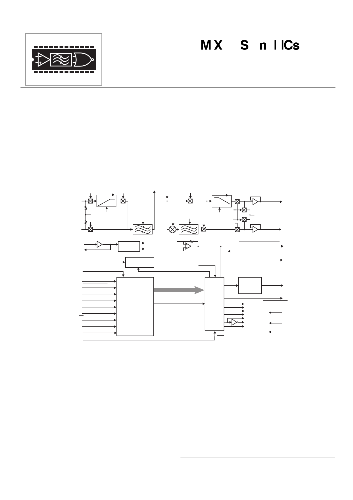
The MX375 is a CMOS LSI microcircuit which combines CTCSS Encode/Decode operation with voice band frequency
inversion. Frequency inversion is achieved by modulating the input audio with a 3333 Hz carrier frequency. Higher voice
band frequencies are translated downward, and lower frequencies upward, resulting in a “mirror image” voice
transmission.
Pvt
SQUELCH
combines CTCSS with inverted speech to prevent users from understanding each other’s
communications unless the transmissions are accompanied by the group’s assigned tone. Its net effect is to eliminate
casual eavesdropping and give mobile radio users a certain degree of privacy at a minimal price. Up to 38
Pvt
SQUELCH
user groups (one per CTCSS tone) can share a single radio channel. With
Pvt
SQUELCH, competing businesses can
share a radio channel without compromising communications security.
Device features: 1) serial or parallel tone programming capability (serial or parallel offered on MX375J, P & LH8), 2) the
ability to operate under NOTONE conditions, 3) on-chip Tx and Rx audio filtering, 4) pin-selectable Private/Clear
operation, and 5) pre/deemphasis filters in the Tx path, for optimal recovered audio quality.
A low-cost 4 MHz crystal/clock and a single 5V supply are required for operation. The MX375 is available in the following
package styles: 28-pin PDIP (MX375P), 28-pin CDIP (MX375J) 28-pin PLCC (MX375LH8), and
24-pin PLCC (MX375LH).

Pvt
SQUELCHTM CTCSS Encoder/Decoder 2 MX375
© 1997 MX•COM Inc. www.mxcom.com Tele: 800 638-5577 910 744-5050 Fax: 910 744-5054 Doc. # 20480026.007
4800 Bethania Station Road, Winston-Salem, NC 27105-1201 USA All trademarks and service marks are held by their respective companies.
CONTENTS
Section Page
1. Block Diagram.................................................................................................................................. 3
2. Signal List......................................................................................................................................... 4
3. External Components...................................................................................................................... 6
4. General Description......................................................................................................................... 7
4.1.1 Pre- and De-emphasis.......................................................................................................................................7
4.1.2 Functions and Outputs.......................................................................................................................................7
5. Application ....................................................................................................................................... 8
5.1.1 CTCSS Programming........................................................................................................................................8
6. Performance Specification.............................................................................................................. 9
6.1 Electrical Performance.............................................................................................................................. 9
6.2 Timing Information ................................................................................................................................... 12
6.2.1 Serial Loading...................................................................................................................................................12
6.2.2 Parallel Loading................................................................................................................................................13
6.3 Packaging ................................................................................................................................................ 13
MX•COM, Inc. reserves the right to change specifications at any time and without notice.

Pvt
SQUELCHTM CTCSS Encoder/Decoder 3 MX375
© 1997 MX•COM Inc. www.mxcom.com Tele: 800 638-5577 910 744-5050 Fax: 910 744-5054 Doc. # 20480026.007
4800 Bethania Station Road, Winston-Salem, NC 27105-1201 USA All trademarks and service marks are held by their respective companies.
1. Block Diagram
3333 Hz
CTCSS
Tone Detect
8-Bit
Shift
Register
and
Latches
Logic
TX Tone
Output
V
V
V
DD
BIAS
SS
PTL
Private
TX Path
RX Path
f
f
f
f
EMPH
CLK2
CLK1
CARRIER
NoTone Output
Control
LD5-LD0
Reference
Hysteresis
RX Tone Decoder Output
Decode Comparator Input
RX Tone Detect Output
Clocks
3333Hz
XTAL
XTAL
RX Tone Input
Load/Latch
D5 or Serial Enable 1
D4 or Serial Enable 2
D3 or Serial Data Input
D2 or Serial Clock Input
D1 Input
D0 Input
RX/TX
Control
Private Enable
Push-To-Listen
BIAS
RX
TX
TX
PVT
CLR
f
f
f
f
f
EMPH
EMPH
CLK1
CARRIER
CLK2
TX Audio
Input
RX Audio
Input
Filter
Output
BIAS
RX
TX
RX Audio Output
TX Audio Output
Balanced
Modulator
Input
6dB/Octave
-6dB/Octave
Filters
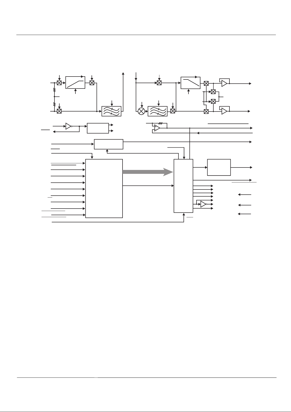
Figure 1: Device Block Diagram

Pvt
SQUELCHTM CTCSS Encoder/Decoder 4 MX375
© 1997 MX•COM Inc. www.mxcom.com Tele: 800 638-5577 910 744-5050 Fax: 910 744-5054 Doc. # 20480026.007
4800 Bethania Station Road, Winston-Salem, NC 27105-1201 USA All trademarks and service marks are held by their respective companies.
2. Signal List
Pin No. Name Type Description
LH J,P,LH8
128 VDDpower 5V supply pin.
2 1 XTAL/CLOCK input This is the input to the clock oscillator inverter. An external 4 MHz Xtal or
clock input should be applied to this pin.
32
XTAL
output This is the 4 MHz output of the clock oscillator inverter.
43
LOAD/
LATCH
input
This input controls the eight input latches: RX/
TX ,
PrivateEnable
, and
D0-D5, as detailed in Table 5. Alternatively, the RX/TX and
PrivateEnable
inputs can be addressed separately by setting the
Load/
Latch
and Control inputs as shown in Table 5. 1 MΩ pullup.
5-7 D4-D2 input
Programming Inputs (Serial Mode Only): These are the
RX/TX tone
programming and function inputs which enable the serial programming
mode. With Load/
Latch
at logic “0” serial data is loaded in the following
sequence: D5, D4, D3, D2, D1, D0, RX/
TX ,
PrivateEnable
. When these
8 bits have been clocked in on the rising clock edge, data is latched by
strobing the Load/
Latch
input “0 - 1 - 0” (See Figure 5).
Pin 5 (D4) =
Serial Enable2
Pin 6 (D3) = Serial Data Input
Pin 7 (D2) = Serial Clock Input
4-9 D5-D0 input
Parallel Programming Inputs: These are the RX/
TX tone programming
and function inputs which select the CTCSS tone (See Table 4).
For both Serial and Parallel Modes:
In RX, a NOTONE program enables
RX Audio Output and forces the RX Tone Decode Output to a logic “0”.
In TX, a NOTONE program generates a constant V
BIAS
-0.7V condition at
the TX Tone Output pin. Each input has a 1 MΩ pullup resistor.
810
RX TONE
DECODE
output The gated output of the decode comparator. In RX, a logic “0” indicates a
valid CTCSS tone decode condition, or the presence of NOTONE
programming. A logic “0” enables the RX audio path. In TX, this output is
held at logic “1”.
9 11 DECODE
COMPARATOR
input The voltage level at this pin is compared internally with a fixed reference
level. A greater input level compared to the reference will result in a logic
“0” at the RX Tone Decode output. This input should be externally
connected to the RX Tone Detect output via external integration
components C10, R2, R3, and D1 (see Figure 2).
10 12 RX TONE
DETECT
output In RX, this pin outputs a logical “1” when a valid programmed CTCSS
tone is received at the RX TONE INPUT. This input should be externally
connected to the Decode Comparator input via external integration
components C10, R2, R3, and D1 (see Figure 2).
N/A 13 NOTONE output This pin outputs a logic “0” when a Notone CTCSS code has been
programmed in RX. It is typically used to enable carrier squelch circuits
under Notone RX conditions.
11 14 V
SS
power The negative supply pin (ground).
12 15 TX TONE
OUTPUT
output The buffered CTCSS sinewave tone output appears on this pin. In TX
mode, the tone frequency is selected by program code (see Table 4); if
NOTONE is programmed, the output is at Vbias-0.7V. In RX mode, the
output goes open circuit. This is an emitter follower output with an
internal 10 kΩ load.

Pvt
SQUELCHTM CTCSS Encoder/Decoder 5 MX375
© 1997 MX•COM Inc. www.mxcom.com Tele: 800 638-5577 910 744-5050 Fax: 910 744-5054 Doc. # 20480026.007
4800 Bethania Station Road, Winston-Salem, NC 27105-1201 USA All trademarks and service marks are held by their respective companies.
Pin No. Name Type Description
LH J,P,LH8
13 16 V
BIAS
This pin is set internally to VDD/2. It must be externally decoupled using a
capacitor (C7) to V
SS
. See Figure 2.
14 17 FILTER
OUTPUT
output This is the output of the Input Audio Bandpass Filter. It must be A.C.
coupled to the Balanced Modulator Input via capacitor C4. See Figure 2.
15 18 BALANCED
MODULATOR
INPUT
input This is the input to the balanced modulator. Must be A.C. coupled to the
Filter Output via capacitor C4. See Figure 2.
16 19 RX AUDIO
OUTPUT
output Outputs the received audio from a buffered output stage and is held at
V
BIAS
when in TX.
17 20 TX AUDIO
OUTPUT
output Outputs the transmitted audio in TX. In RX, this pin is held at V
BIAS
.
18 21 RX AUDIO
INPUT
input The audio input for the RX mode. Input signals should be AC coupled via
external capacitor C6. See Figure 2
19 22 TX AUDIO
INPUT
input This is the TX Audio voice input. Signals should be AC coupled via
external capacitor C11. See Figure 2
20 23
PTL
input The “press to listen” function input. In RX mode, a logic “0” enables the
RX Audio Output directly, overriding tone squelch but not intercepting a
private conversation; in TX mode, a logic “0” reverses the phase of the TX
Tone Output for “squelch tail” reduction (see Table 5).
21 24 CONTROL
This input, together with Load/
Latch
, selects the operational mode of the
RX/
TX and
PrivateEnable
functions. See Table 5
22 25
RX/
TX
input This input selects the RX or TX mode (RX = 1, TX = 0). This can be
loaded in Serial or Parallel modes as described in Table 5
23 26
PRIVATE
ENABLE
This input selects either Private or Clear mode (Clear = 1, Private = 0),
and can be loaded by Serial or Parallel modes as described in Table 5.
This input has an internal 1 MΩ pullup resistor.
24 27 RX TONE
INPUT
input This is the received audio input to the on-chip CTCSS tone decoder. It
should be A.C. coupled via capacitor C5.
Note: The MX375LH package is available in serial mode only.
Table 1: Signal List
 Loading...