

MX COM Inc MX214J, MX224P, MX224J, MX214P, MX214LH Datasheet
...
DATA BULLETIN
Variable Split Band
MX214/224
Features Applications
CTCSS Highpass Filter
Good Recovered Audio Quality
Fixed and Rolling Code Modes
Serial (MX214) and Parallel (MX224)
Loading Options
32 Programmable Split Points
Half-Duplex Capability
POWERSAVE
LOAD / LA TC H
SERIAL CLOCK
ENABLE / MUTE
CLEAR / SCRAMBLE
Rx / (SER / PAR)Tx
A0
A1
A2
A3
A4
(SERIAL DATA IN)
Rx IN
Tx IN
PS
PS
INPUT LATCHES
BIAS
BIAS
EN Rx⋅⋅PS
Rx
MUTE
Tx ⋅ PS
Tx ⋅ PS
BIAS
CK
FILTER 3
CK
3
A
EN / MUTE
CLEAR / SCRAMBLE
Rx / Tx
CTCSS
C
5
Rx
Tx
C6
ROM
Mobile Radio Voice Security
Cellular Telephone Voice
Security
1MHz
OSC
1MHz
PS
3
PS EN Tx⋅⋅
Tx
SCRAMBLE
CLOCK
DIVIDER
CK
B
CLOCK
SWITCHING
Tx
Rx
BIAS
CLOCK
DIVIDER
FC1F
CK
C2
A
CK
Rx
Rx
FILTER 4
FILTER 2FILTER 1
CK4
CK
4
CK
A
CK
B
F
C2
F
C1
Rx
Tx
Inverter
CK
B
Rx / Tx
Σ
CK
4
CLEAR
PS + EN Rx⋅
XTAL / CLOCK
PS + EN Tx⋅
BIAS
PS MUTE Rx⋅⋅
BIAS
BIAS
XTAL
V
DD
V
BIAS
V
SS
Tx OUT
Rx OUT
The MX214/224 Variable Split Band Inverters are designed for mobile and cellular radio voice security
applications. Digital control functions are loaded serially into the MX214. The MX224 is loaded in parallel.
The MX214/224 ICs include a highpass filter that rejects subaudio frequencies, ensuring full CTCSS
compatibility. This CTCSS filter is not included on the earlier generation MX204 VSB Inverter.
The MX214/224 splits the voiceband (300-2700Hz) into upper and lower subbands, and inverts each subband
about itself. The ‘split point’ (defined as the frequency where the voice band is subdivided), is externally
programmable to 32 distinct values in the 300 to 3000Hz range. In the ‘fixed code’ mode, a single point is
used. Fixed mode operation nets approximately 4 mutually exclusive secure channels.
In ‘rolling code’ mode, the split point is changed many times per second, usually under control of a
microprocessor. Rolling code scrambling requires synchronization, offers higher security than fixed code
operation, and provides a much greater number of mutually exclusive secure channels.
The MX214/224 offers a recovered audio product close to that of a telephone. The on-chip ‘ Mute’ function is
useful when implementing rolling code continuous synchronization schemes. ‘Powersave’ and
‘Clear/Scramble’ controls are also included on-chip. Timing and filter clocks are derived internally from an
on-chip 1MHz reference oscillator driven by a 1MHz crystal or clock pulse input.
The MX214 and the MX224 operate from a single 5.0V supply and available in the following packges:
22-pin CDIP (MX214J/MX224J), 22-pin PDIP (MX214P/MX224P), and 24-pin PLCC (MX214LH/MX224LH).
1998 MX-COM, Inc. www.mxcom.com Tel: 800 638 5577 336 744 5050 Fax: 336 744 5054 Doc. # 20480112.002
4800 Bethania Station Road, Winston-Salem, NC 27105-1201 USA All trademarks and service marks are held by their respective companies.

Variable Split Band Inverter 2 MX214/224
Contents
Section Page
1. Block Diagram................................................................................................................3
2. Signal List.......................................................................................................................4
3. External Components....................................................................................................7
4. General Description.......................................................................................................8
5. Application .....................................................................................................................9
5.1 Audio Quality.......................................................................................................................... 9
6. Performance Specifications........................................................................................11
6.1 Electrical Specifications........................................................................................................ 11
6.1.1 Absolute Maximum Limits.......................................................................................................11
6.1.2 Operating Limits......................................................................................................................11
6.1.3 Operating Characteristics .......................................................................................................12
6.1.4 Timing.....................................................................................................................................14
6.2 Packages.............................................................................................................................. 15
MX-COM, Inc. reserves the right to change specifications at any time without
notice.
1998 MX-COM, Inc. www.mxcom.com Tel: 800 638 5577 336 744 5050 Fax: 336 744 5054 Doc. # 20480112.002
4800 Bethania Station Road, Winston-Salem, NC 27105-1201 USA All trademarks and service marks are held by their respective companies.
Variable Split Band Inverter 3 MX214/224
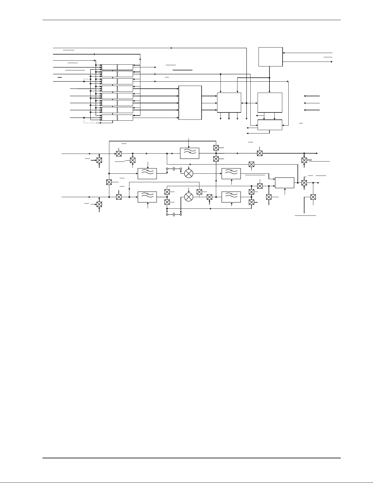
1. Block Diagram
POWERSA VE
LOAD / LATCH
SERIAL CLOCK
ENABLE / MUTE
CLEAR / SCRAMBLE
Rx / (SER / PAR)Tx
A0
A1
A2
A3
A4
(SERIAL DATA IN)
Rx IN
Tx IN
PS
PS
INPUT LATCHES
BIAS
Tx ⋅ PS
Tx ⋅ PS
BIAS
EN Rx⋅⋅PS
Rx
MUTE
BIAS
CK
3
FILTER 3
CK
A
EN / MUTE
CLEAR / SCRAMBLE
Rx / Tx
ROM
CK
CTCSS
C
5
Rx
Tx
C6
Rx / Tx
4
PS + EN Rx⋅
BIAS
BIAS
XT AL / CLOCK
XT AL
V
DD
V
BIAS
V
SS
Tx OUT
PS + EN Tx⋅
PS MUTE Rx⋅⋅
Rx OUT
BIAS
1MHz
OSC
1MHz
CLOCK
DIVIDER
CK
CK
C2
CK
CK4
4
A
PS
3
SCRAMBLE
FC1F
CK
A
B
Rx
Rx
F
C2
FILTER 4
F
C1
Rx
FILTER 2FILTER 1
Tx
CLOCK
DIVIDER
CLOCK
SWITCHING
PS EN Tx⋅⋅
Tx
Tx
Rx
BIAS
CK
B
CLEAR
CK
B
Σ
CK
Figure 1: Block Diagram
1998 MX-COM, Inc. www.mxcom.com Tel: 800 638 5577 336 744 5050 Fax: 336 744 5054 Doc. # 20480112.002
4800 Bethania Station Road, Winston-Salem, NC 27105-1201 USA All trademarks and service marks are held by their respective companies.
Variable Split Band Inverter 4 MX214/224
2. Signal List
MX214
Pin No.
MX224
Pin No.
Signal Name Description
J/P LH J/P LH
7 1 1 1 Xtal/Clock Input to the clock oscillator inverter. A 1MHz crystal
input or externally derived 1MHz clock is injected
here.
822 2
Xtal
Output of the clock oscillator inverter.
9 3 Serial Data Input This pin is used to input an 8-bit word representing
the digital control functions. This word is loaded
using the serial data clock and in input in the
following sequence: MUTE, CLEAR,
A1, A2, A3, A4. The
is operated on the
Latch/Load
Tx/Rx , A0,
completion. Reference the timing diagram in Figure
8.
3 – A4
4 – A3
5 – A2
6 – A1
7 – A0
3 – A4
4 – A3
5 – A2
6 – A1
7 – A0
88
Programming
Inputs
Tx/Rx
In parallel mode, these five digital inputs define the
split point frequency. Each of the 5 input pins has a
1M internal pull-up resistor. See Table 4 for
programming information.
This digital input selects the Receive and Transmit
paths and configures upperband and lowerband
filter bandwidths while setting the CTCSS highpass
filter position on the signal path. See Table 2,
Figure 6, and Figure 7. 1M internal pull-up resistor
(Rx).
13 8
Serial/Parallel
This pin must be connected to V
for serial loading.
SS
Internal 1M pull-up resistor.
9 9 Clear/Scramble This digital input puts the device into ‘Clear’ or
‘Scramble’ mode by controlling the application of
carrier frequency to the Upper and Lower band
balanced modulators. In ‘Scramble’ mode, the
balanced modulator carrier frequency values are
selected by the split point address A0-A4. See
Table 4. In ‘Clear’ mode, the carriers are disabled
and the balanced modulators are bypassed
internally, i.e. the lower band signal is not added to
the output signal. 1MHz internal pull-up resistor
(Clear).
10 10 Enable/Mute This digital function is used to disable the Receive or
the Transmit signal paths for rolling code
synchronization while maintaining bias conditions.
Synchronization data can be transmitted during the
Mute periods, as is done in the MX1204 VSB
Scrambler Module. 1M Internal pull-up resistor
(Enable)
14 10 Serial Clock
Input
This is the externally applied data clock frequency
used to shift input data along in devices wired in the
Serial-loading mode. One full data clock cycle is
required to shift one data bit completely into the
register. See Timing Diagram Figure 8. 1M
Internal pull-up resistor.
1998 MX-COM, Inc. www.mxcom.com Tel: 800 638 5577 336 744 5050 Fax: 336 744 5054 Doc. # 20480112.002
4800 Bethania Station Road, Winston-Salem, NC 27105-1201 USA All trademarks and service marks are held by their respective companies.
Variable Split Band Inverter 5 MX214/224
MX214
Pin No.
MX224
Pin No.
Signal Name Description
J/P LH J/P LH
15 11 11 11
Latch/Load
This pin controls the loading of the 8 digital function
inputs (ENABLE, CLEAR, A0-A4) into the internal
register. When this pin is at a logic ‘1’, all eight
inputs are transparent and new data acts directly.
For controlled changing of parameters in the
parallel,
Latch/Load must be kept at logic ‘0’ while
a new function is loaded, then strobed 0-1-0 to latch
the inputs in. For serial loading, the serial data
should be loaded with the
and then the
Latch/Load strobed 0-1-0 on
Latch/Load at logic ‘0’
completion of data loading. Internal 1M pull-up
resistor (Load). See Figure 8.
16 12 12 12 Powersave This digital input is used to place the MX214/224
into Powersave mode where all parts of the device
except the 1MHz oscillator are shut down. All signal
input and output lines are made open circuit, free of
all bias. This allows signal paths to be routed
externally around the device, while reducing current
consumption. A logic ‘0’ at this input enables the
device to work normally as shown in Table 2.
Internal 1M pull-up resistor.
17 13 13 13 V
SS
Negative supply (GND)
18 14 14 14 Internal connection This pin is internally connected. Leave open circuit.
19 15 15 15 Rx Output This is the processed received audio signal output.
This pin is held at a DC ‘bias’ voltage for all
functions except Powersave. This buffered output is
driven by the summing circuit in the Rx mode.
Signal paths and bias levels are detailed in Table 2
and Figure 7.
20 16 16 16 Tx Output This is the processed audio output for the
transmission channel. This pin is held at a DC ‘bias’
voltage for all functions except Powersave. This
summed and buffered signal is passed through the
CTCSS high pass Filter to the output pin in the Tx
Mode. Signal paths and bias levels are detailed in
Table 2 and Figure 6.
21 17 17 17 V
BIAS
Normally at VDD/2, this pin requires an external
decoupling capacitor (C7) to V
SS
.
22 18 18 18 Rx Input This is the analog received signal input. This pin is
held at a DC ‘bias’ voltage by a 300k on-chip bias
resistor, which is selected for all functions except
Powersave. It must be connected to external
circuitry by capacitor C3. See Figure 2 and Figure
3. This input is routed through the CTCSS High
Pass Filter in Rx mode to remove subaudio
frequencies from the voiceband. Signal paths and
bias levels are detailed in Table 2 and Figure 7.
1 19 19 19 Highband Filter
Output
The output of the Input Filter of the Upperband limit.
The
Tx/Rx functions sets the lowpass filter at
3400Hz or 2700Hz respectively. This output must
be connected to the Highband Balanced modulator
input via capacitor C5. See Figure 2 and Figure 3.
1998 MX-COM, Inc. www.mxcom.com Tel: 800 638 5577 336 744 5050 Fax: 336 744 5054 Doc. # 20480112.002
4800 Bethania Station Road, Winston-Salem, NC 27105-1201 USA All trademarks and service marks are held by their respective companies.
 Loading...