

MX COM Inc MX165CTN, MX165CP, MX165CLH, MX165CDW Datasheet
DATA BULLETIN
MX165C
© 1997 MX
•COM Inc. www.mxcom.com Tele: 800 638-5577 910 744-5050 Fax: 910 744-5054 Doc. # 20480102.008
4800 Bethania Station Road, Winston-Salem, NC 27105-1201 USA
All trademarks and service marks are held by their respective companies.
Low Voltage
CTCSS Encoder/Decoder
with TX/RX Filters
Features Applications
•
Meets TIA/EIA-603 Standards
•
47 CTCSS Tones + Notone
•
TX/RX Speech Filters
•
Improved Sinad
•
Serial or Parallel Programming
•
Easy µP Interface
•
Scanning on any Channel
•
Standard 1MHz Xtal
(See MX465 for 4MHz)
•
Low Voltage 3.3V to 5.0V
•
Mobile Radio Channel Sharing
•
Scan Trunking
•
Wireless Intercom Traffic Control
•
Hookswitch Supervision
•
Repeater Control
DIGITAL
INTERFACE
AND
CLOCK
GENERA TION
+
+
+
-
-
-
LOAD/
D5/SERIAL ENABLE 1
D3/SERIAL DATA IN
D2/SERIAL CLOCK
LA TCH
D4/SERIAL ENABLE 2
D1
D0
RX/
PTL
TX
DECODE COMPARA T OR REF.
DECODE COMPARA T OR IN
RX TONE DETECT
RX TONE DECODE
TX TONE OUT
TONE DETECT
LOGIC
TONE
ROM
48 x 10
RX AUDIO OUT
TX AUDIO OUT
TONE
f
300Hz
TONE IN
RX AUDIO IN
TX AUDIO IN
XT AL/CLK
XT AL
A0-A5
D0-D10
CLK
CLKS
CLKS
CLKS/XTAL
CLKS/XTAL
REFERENCE
VOLTAGE
TONE IN
FILTER
TONE DECODE
FILTER
TONE OUT FIL TER
AUDIO FILTER
V
V
V
DD
SS
BIAS
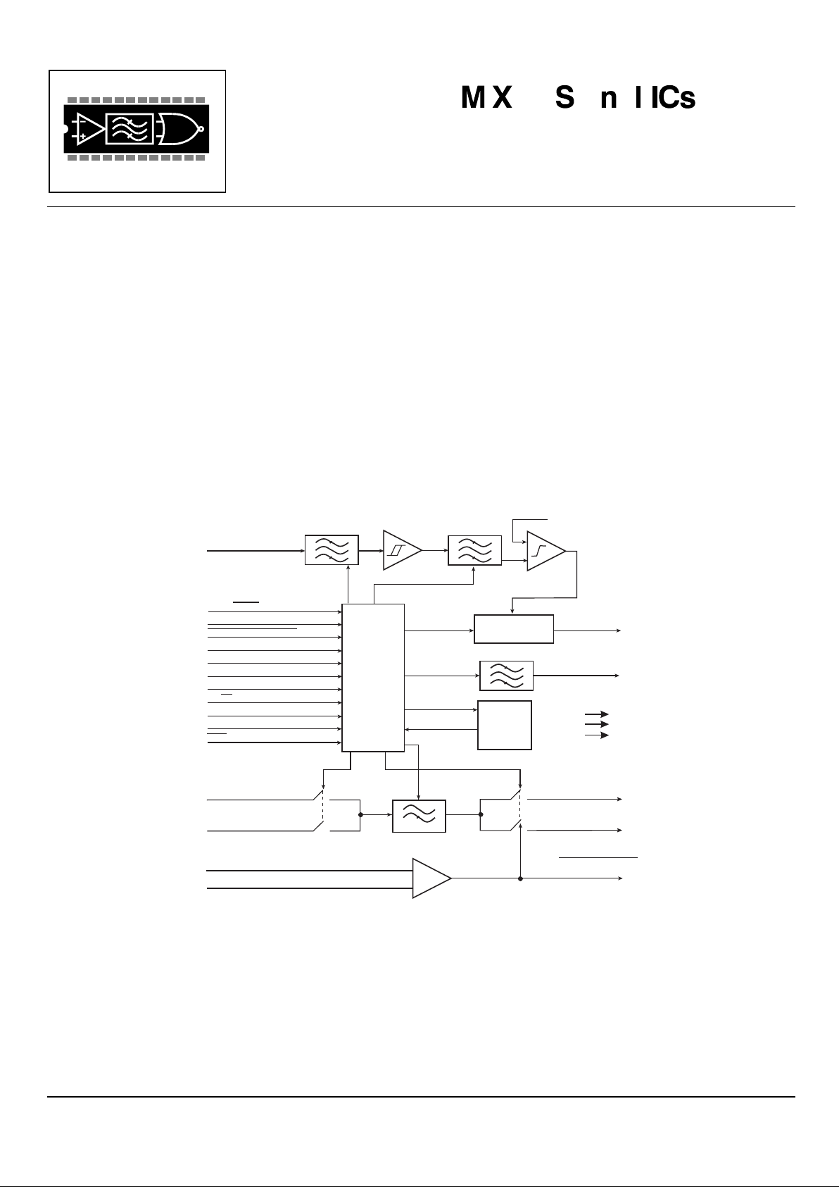
The MX165C CTCSS Encoder/Decoder is a low voltage, CMOS device that meets TIA/EIA-603 Standards. The MX165C
will encode and decode the tones 159.8Hz, 183.5Hz, 189.9Hz, 196.6Hz, 199.5Hz, 206.5Hz, 229.1Hz, and 254.1Hz in
addition to the 39 standard CTCSS tones, for a total of 47 CTCSS tones + Notone. With the incorporation of the on-chip
TX and RX speech filter, the MX165C enhances voice/tone multiplexing by attenuating TX and RX speech 36dB at
frequencies below 250Hz while passing signals > 300Hz with only 1dB of ripple. This not only minimizes CTCSS talk-off
in the TX mode but also improves Hum and Noise performance in the RX mode.
Available in the following package styles: 24-pin TSSOP (MX165CTN), 24-pin SOIC (MX165CDW), 24-pin PLCC
(MX165CLH), and 24-pin PDIP (MX165CP), the MX165C requires a single 3.3V to 5.0V supply and a 1MHz clock or
crystal.

Low Voltage CTCSS Encoder/Decoder 2 MX165C
© 1997 MX•COM Inc. www.mxcom.com Tele: 800 638-5577 910 744-5050 Fax: 910 744-5054 Doc. # 20480102.008
4800 Bethania Station Road, Winston-Salem, NC 27105-1201 USA
All trademarks and service marks are held by their respective companies.
CONTENTS
Section Page
1. Block Diagram.................................................................................................................................. 3
2. Signal List......................................................................................................................................... 4
3. External Components...................................................................................................................... 6
4. General Description......................................................................................................................... 7
4.1 Description................................................................................................................................................ 7
4.2 I/O Conditions ........................................................................................................................................... 7
4.3 Filter Response......................................................................................................................................... 8
4.4 Serial and Parallel Mode Timing............................................................................................................... 8
4.5 CTCSS Programming .............................................................................................................................. 10
5. Performance Specification............................................................................................................. 11
5.1 Electrical Performance............................................................................................................................. 11
5.1.1 Absolute Maximum Ratings..............................................................................................................................11
5.1.2 Operating Limits................................................................................................................................................11
5.2 Packaging ................................................................................................................................................ 14
MX•COM, Inc. Reserves the right to change specifications at any time and without notice
Low Voltage CTCSS Encoder/Decoder 3 MX165C
© 1997 MX•COM Inc. www.mxcom.com Tele: 800 638-5577 910 744-5050 Fax: 910 744-5054 Doc. # 20480102.008
4800 Bethania Station Road, Winston-Salem, NC 27105-1201 USA
All trademarks and service marks are held by their respective companies.
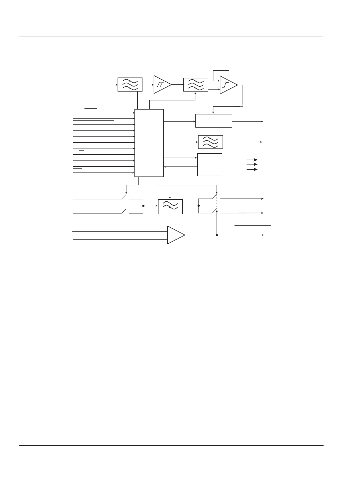
Block Diagram
DIGITAL
INTERFACE
AND
CLOCK
GENERA TION
+
+
+
-
-
-
LOAD/
D5/SERIAL ENABLE 1
D3/SERIAL DATA IN
D2/SERIAL CLOCK
LATCH
D4/SERIAL ENABLE 2
D1
D0
RX/
PTL
TX
DECODE COMPARAT OR REF.
DECODE COMPARAT OR IN
RX TONE DETECT
RX TONE DECODE
TX TONE OUT
TONE DETECT
LOGIC
TONE
ROM
48 x 10
RX AUDIO OUT
TX AUDIO OUT
TONE
f
300Hz
TONE IN
RX AUDIO IN
TX AUDIO IN
XTAL/CLK
XTAL
A0-A5
D0-D10
CLK
CLKS
CLKS
CLKS/XTAL
CLKS/XTAL
REFERENCE
VOLTAGE
TONE IN
FILTER
TONE DECODE
FILTER
TONE OUT FILTER
AUDIO FILTER
V
V
V
DD
SS
BIAS
Figure 1 : Block Diagram
Low Voltage CTCSS Encoder/Decoder 4 MX165C
© 1997 MX•COM Inc. www.mxcom.com Tele: 800 638-5577 910 744-5050 Fax: 910 744-5054 Doc. # 20480102.008
4800 Bethania Station Road, Winston-Salem, NC 27105-1201 USA
All trademarks and service marks are held by their respective companies.
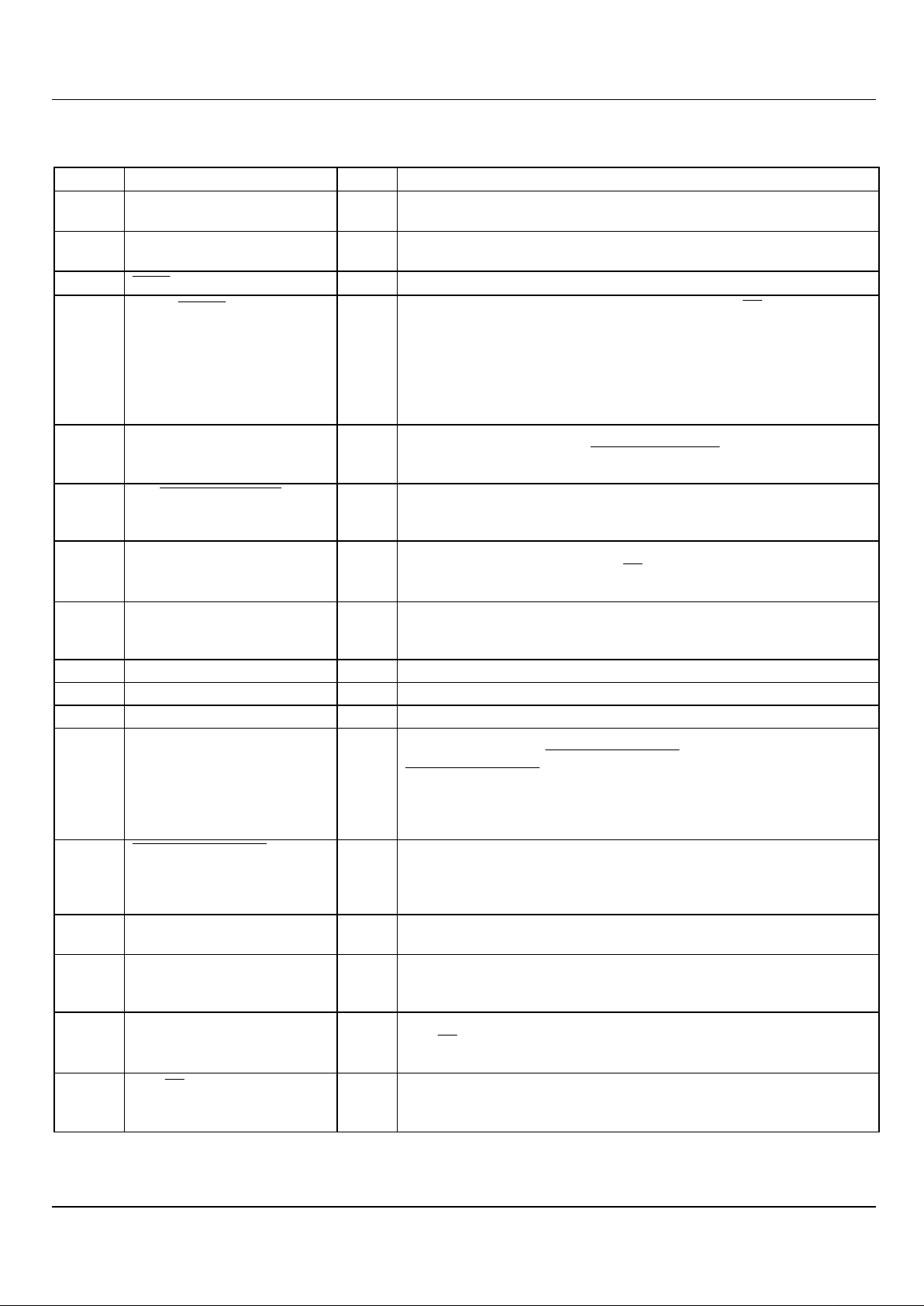
Signal List
Pin No. Signal Type Description
1V
DD
power Positive supply. This pin should be bypassed to VSS by a capacitor
mounted close to the device pins.
2 XTAL/CLOCK input Input to the on-chip inverter used with a 1MHz Xtal or external clock
source.
3
XTAL
output Output of the on-chip inverter (clock output).
4
LOAD/LATCH
input
Controls 8 on-chip latches. It is used to latch
RX TX/
, PTL, and D0D5. A logic 1 applied to this input places the 8 latches in the
‘transparent’ mode. A logic 0 applied to this input places the 8 latches
in the ‘latched’ mode. In Parallel Mode, data is loaded and latched by
a logic 1-0 transition (see Figure 4). In Serial Mode, data is loaded
and latched by a 0-1-0 strobe pulse on this pin (see Figure 5).
Internally pulled to V
DD
5 D5 / SERIAL ENABLE 1 input Data input D5 (Parallel Mode). A logic 1 applied to this input together
with a logic 0 applied to
D4/SERIAL ENABLE 2
will place the device
in Serial Mode (see Figure 5). Internally pulled to V
DD
.
6
D4 / SERIAL ENABLE 2
input Data input D4 (Parallel Mode). A logic 0 applied to this input together
with a logic 1 applied to D5 / SERIAL ENABLE 1 will place the device
in Serial Mode (see Figure 5). Internally pulled to V
DD
.
7 D3 / SERIAL DATA IN input Data input D3 (Parallel Mode). In Serial Mode this pin becomes the
serial data input for D5-D0,
RX / TX
and PTL (see Figure 5). D5 is
clocked first and PTL last. Internally pulled to V
DD
.
8 D2 / SERIAL CLOCK input Data input D2 (Parallel Mode). In Serial Mode this pin becomes the
SERIAL CLOCK input. Data is clocked on the positive going edge
(see Figure 5). Internally pulled to V
DD
.
9 D1 input Data input D1 (Parallel Mode). Internally pulled to VDD.
10 D0 input Data input D0 (Parallel Mode). Internally pulled to VDD.
11 V
SS
power Negative supply.
12 DECODE COMPARATOR
REF.
input Internally biased to VDD/3 or 2 VDD/3 via 1M resistors depending on
the logic state of the
RX TONE DECODE pin.
RX TONE DECODE = 1 will bias this input 2 VDD/3; a logic 0 will bias
this input V
DD
/3. This input provides the DECODE COMPARATOR
REFERENCE voltage, and the switching of bias voltages provides
hysteresis to reduce ‘chatter’ under marginal conditions.
13
RX TONE DECODE
output Gated output of the decode comparator. This output is used to gate
the RX Audio path. A logic 0 on this pin indicates a successful
decode and the DECODE COMPARATOR IN pin is more positive
than the DECODE COMPARATOR REF. input (see Table 3).
14 DECODE COMPARATOR IN input Inverting input of the DECODE COMPARATOR. This pin is normally
connected to the integrated output of the RX TONE DETECT line.
15 RX TONE DETECT output In RX mode this output will go to logic 1 during a successful decode.
It must be externally integrated to control response and deresponse
times (see Table 3).
16 TX TONE OUT output The CTCSS sinewave output appears on this pin under control of the
RX / TX
pin. When not transmitting a tone, TX TONE OUT may be
biased to V
DD
/2. (see Table 3).
17
RX / TX
input RX or TX modes selected in Parallel Mode (see Figure 4). In Serial
Mode this function is serially loaded. This pin is internally pulled to
V
DD
via a 1MΩ resistor.
Low Voltage CTCSS Encoder/Decoder 5 MX165C
© 1997 MX•COM Inc. www.mxcom.com Tele: 800 638-5577 910 744-5050 Fax: 910 744-5054 Doc. # 20480102.008
4800 Bethania Station Road, Winston-Salem, NC 27105-1201 USA
All trademarks and service marks are held by their respective companies.
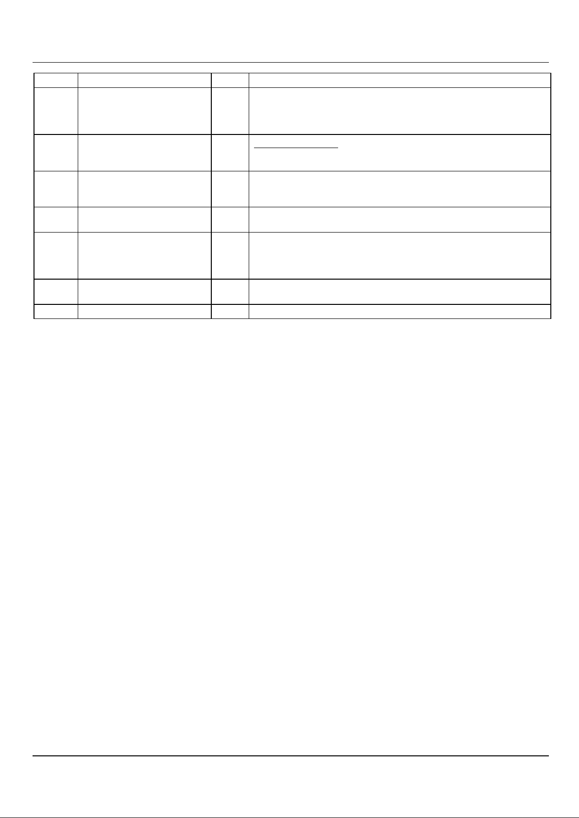
Pin No. Signal Type Description
18 PTL input In RX mode this pin operates as a ‘Push To Listen’ function by
enabling the RX audio path, thus overriding the tone squelch function
(Parallel Mode). In Serial Mode this function is loaded serially.
Internal pull-up to V
DD
19 RX AUDIO OUT output High pass filtered RX AUDIO OUT. This pin outputs audio when
RX TONE DECODE = logic 0, PTL = logic 1, or when Notone is
programmed (see Table 4). In TX mode this pin is biased to V
DD
/2.
20 TX AUDIO OUT output High pass filtered TX AUDIO OUT pin. In TX mode this pin outputs
audio present at the TX AUDIO IN pin. In RX mode this pin is biased
to V
DD
/2
21 V
BIAS
output Output of an internally generated VDD /2 bias level that would
normally be externally bypassed to V
SS
via capacitor C6.
22 TX AUDIO IN input In TX mode TX AUDIO IN may be prefiltered, using the TX Audio
path, thus helping to avoid talk-off due to intermodulation of speech
frequencies with the transmitted CTCSS tone. Internally biased to
V
DD
/2.
23 RX AUDIO IN input Input to the audio high pass filter in RX mode. Internally biased to
V
DD
/2.
24 TONE INPUT input Input to the CTCSS tone detector. Internally biased to VDD/2.
Table 1: Signal List
 Loading...