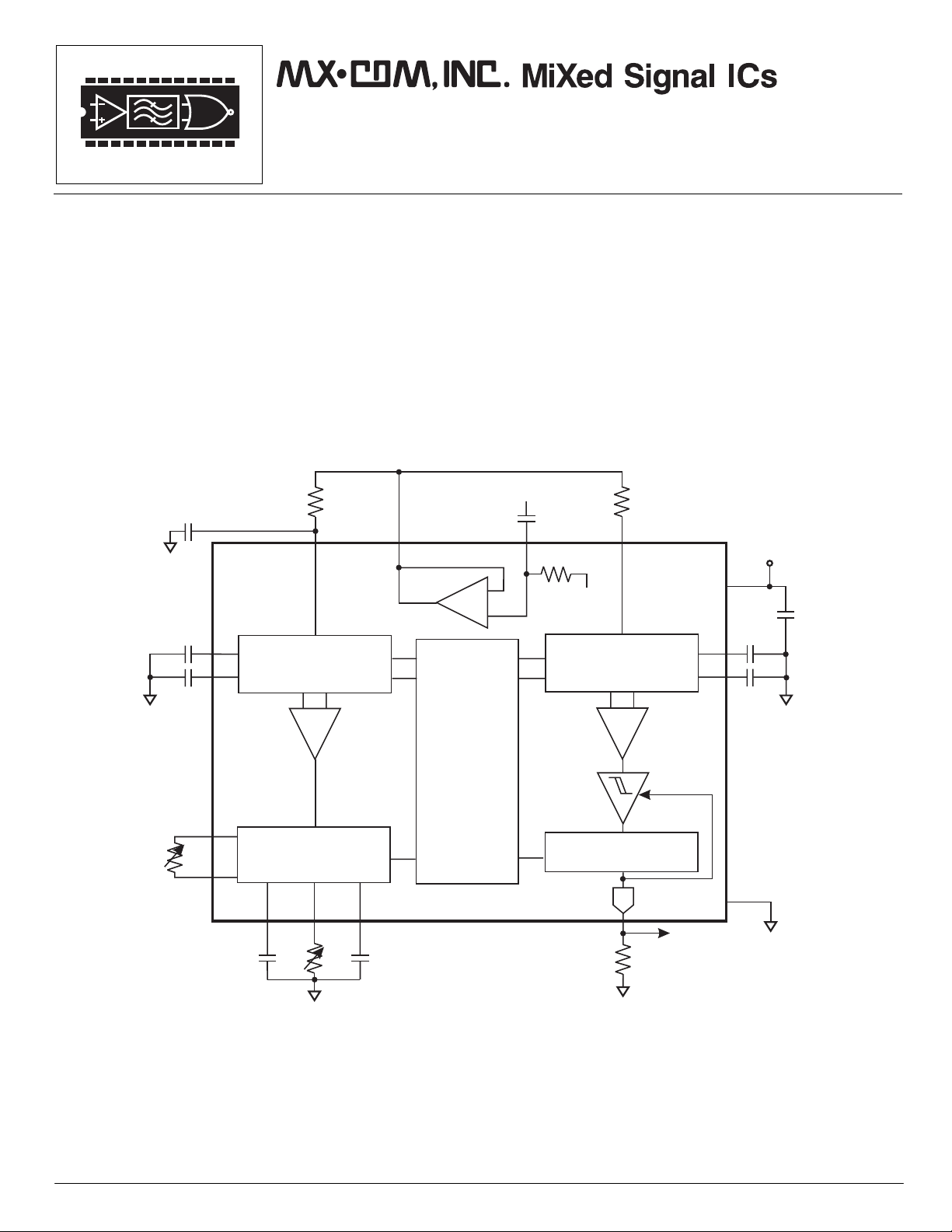
MX COM Inc MX105ALH, MX105AP, MX105ADW Datasheet

DATA BULLETIN
MX105A
FEATURES
•
Operates in High Noise Conditions
•
36 dB Signal Input Range
• ≥
High Sensitivity
•
Low Power Operation 2.7 V to 5.5 V
•
Adjustable Bandwidth
•
Adjustable Frequency
•
C4
C2
C2
A
7
8
B
R2
4
Loop
Filter
-
+
2
Input Amp
-
+
Timing
Logic
Tone Detector
PRELIMINARY INFORMATION
APPLICATIONS
•
Single and Multitone System
•
Applications
Tone In
1
C5
V/2
DD
3
Detect
Filter
+
-
R3
16
V
DD
C6
C3
A
5
6
C3
B
11
R4
12
VCO
1513
14
MX105A
Detect Counter
9
10
Detect
C1
The MX105A is a monolithic CMOS tone detector for tone decoding in single and multitone signaling systems. Using
phase locked loop (PLL) decoding techniques, the MX105A recognizes tones in the presence of high noise levels and
strong adjacent channel tones. Detection frequency and bandwidth can each be independently adjusted. The design is
immune to high levels of harmonic and sub-harmonic noise. It also maintains excellent noise immunity and constant
bandwidth over a wide range of input signal levels.
The MX105A requires a voltage supply of 2.7V to 5.5V and is available in the following package styles: 16-pin SOIC
(MX105ADW), 16-pin PDIP (MX105AP), and 24-pin PLCC (MX105ALH).
© 1997 MX•COM, INC. www.mxcom.com Tele: 800 638 5577 910 744 5050 Fax: 910 744 5054 Doc.# 20480133.003
4800 Bethania Station Road, Winston-Salem, NC 27105-1201 USA All trademarks and service marks are held by their respective companies.
R1
B
C1
A
R
L
Out

Tone Detector 2 MX105A PRELIMINARY INFORMATION
CONTENTS
Section..........................................................................................................................Page
1. Block Diagram ................................................................................................................3
2. Signal List .......................................................................................................................4
3. External Components ....................................................................................................5
4. General Description .......................................................................................................6
5. Application......................................................................................................................7
5.1 Method for Calculating External Component Values...............................................................7
5.2 Define f0..................................................................................................................................7
5.3 Calculate Minimum Usable Bandwidth....................................................................................7
5.4 Calculate The Recommended Operating Bandwidth..............................................................7
5.5 Select R4 for Operating BW....................................................................................................8
5.6 Calculate R2×C2A...................................................................................................................8
5.7 Define Maximum Allowed Response Time..............................................................................8
5.8 Calculate R3×C3A...................................................................................................................8
5.9 Calculate Maximum De-response Time..................................................................................9
5.10 Calculate Signal to Noise Performance...............................................................................10
5.11 Calculate C4 for 30° Phase Shift.........................................................................................10
6. Performance Specification ..........................................................................................11
6.1 Electrical Performance..........................................................................................................11
6.1.1 Absolute Maximum Ratings..........................................................................................................11
6.1.2 Operating Limits............................................................................................................................11
6.1.3 Operating Characteristics.............................................................................................................12
6.2 Packaging..............................................................................................................................13
MX•COM, Inc. reserves the right to change specifications at any time and without notice.
© 1997 MX•COM, INC. www.mxcom.com Tele: 800 638 5577 910 744 5050 Fax: 910 744 5054 Doc.# 20480133.003
4800 Bethania Station Road, Winston-Salem, NC 27105-1201 USA All trademarks and service marks are held by their respective companies.

Tone Detector 3 MX105A PRELIMINARY INFORMATION
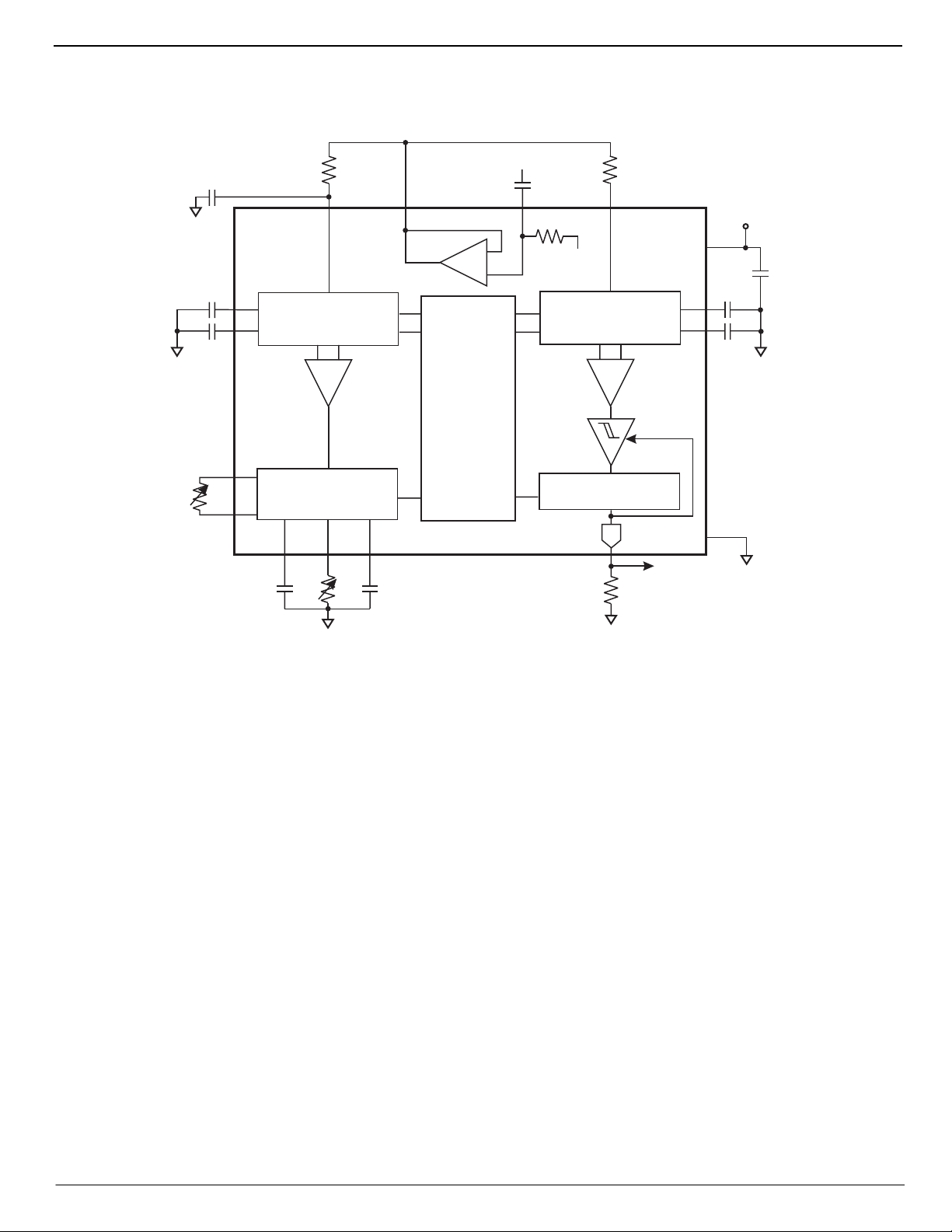
1. Block Diagram
R4
C4
C2
C2
R2
Tone In
R3
C5
V
C3
C3
DD
C6
A
B
4
2
Input Amp
-
+
A
7
8
B
11
12
Loop
Filter
-
VCO
1513
+
14
Timing
Logic
MX105A
1
V/2
DD
Detect Counter
3
Detect
Filter
+
-
9
16
5
6
10
Detect
C1
R1
B
C1
A
R
L
Out
Figure 1: Block Diagram
© 1997 MX•COM, INC. www.mxcom.com Tele: 800 638 5577 910 744 5050 Fax: 910 744 5054 Doc.# 20480133.003
4800 Bethania Station Road, Winston-Salem, NC 27105-1201 USA All trademarks and service marks are held by their respective companies.

Tone Detector 4 MX105A PRELIMINARY INFORMATION
2. Signal List
Pin No. Pin No. Name Type Description
DW/P LH
1 1 INPUT AMP IN input AC couple to this input. Nominal input
impedance is 200 kΩ.
2 3 INPUT AMP OUT output
3 5 R3 input Detect filter resistor pin.
4 6 R2 input PLL loop filter resistor pin. For improved
57 C3
68 C3
710 C2
811 C2
A
B
A
B
output Detect filter capacitor pin A
output Detect filter capacitor pin B
output Loop filter capacitor pin A
output Loop filter capacitor pin B
9 13 DETECT OUT output PMOS open drain output - active on detect.
10 14 V
11 16 R4
12 17 R4
13 19 C1
14 20 C1
SS
A
B
B
A
power Ground.
input Bandwidth control resistor pin A
input Bandwidth control resistor pin B
output VCO capacitor B
output VCO capacitor A
15 22 R1 input VCO discharge resistor. When potentiometer
16 24 V
DD
power Power supply.
Nominal output impedance is 1 kΩ.
performance C4 may be chosen to provide 30°
of phase shift at the loop filter input.
tuning is required, a series resistor is
recommend to prevent possible shorting to
ground.
© 1997 MX•COM, INC. www.mxcom.com Tele: 800 638 5577 910 744 5050 Fax: 910 744 5054 Doc.# 20480133.003
4800 Bethania Station Road, Winston-Salem, NC 27105-1201 USA All trademarks and service marks are held by their respective companies.

Tone Detector 5 MX105A PRELIMINARY INFORMATION
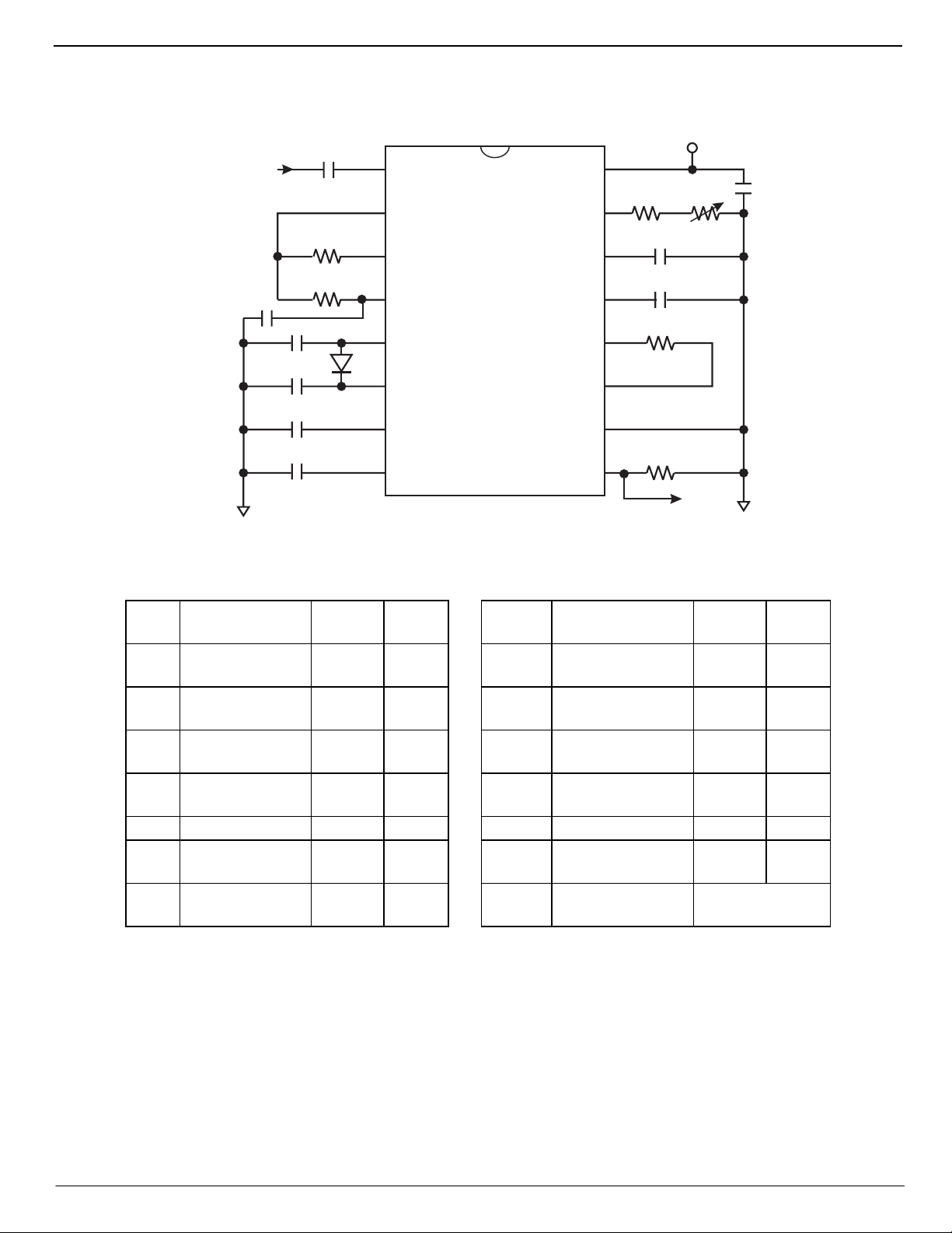
3. External Components
V
R1
DD
C6
V
Signal Input
C4
C3
C3
C2
C2
C5
1
2
R3
3
R2
4
MX105A
5
A
B
A
B
D1
6
7
8
16
15
14
13
12
11
10
R1
F
C1
A
C1
B
R4
V
SS
R
L
9
Detect Out
Figure 2: Recommended External Components
R1
See Section 5.2
F
300k
Ω
C2
See section 5.6
A
Note 2
R1
See Section 5.2
V
100k
Ω
C2
See Section 5.6
B
Note 2
R2 See Section 5.6 C3
See Section 5.8
A
Note 2
R3 See Section 5.8 C3
See Section 5.8
B
Note 2
R4 See Section 5.5 C4 See Section 5.11
Note 1, 2
R
C1
L
A
Note 4
See Section 5.2
20k
±20% C5 0.27µF ±20%
Ω
C6 0.1µF ±20%
Note 2
C1
See Section 5.2
B
Note 2
D1 See Section 5.9
Note 3
small signal
diode (1N914)
External Components Notes:
1. For improved performance, C4 may be chosen to provide 30° phase shift at the VCO loop filter input.
2. For compatibility with the MX105; capacitors (C1 - C4) may be connected to V
instead of VSS.
DD
3. For improved de-response time, a diode (D1) may be added.
4. Any value load resistance (R
) may be used, providing the maximum load current does not exceed the value
L
given in ‘Maximum Ratings Specifications’.
© 1997 MX•COM, INC. www.mxcom.com Tele: 800 638 5577 910 744 5050 Fax: 910 744 5054 Doc.# 20480133.003
4800 Bethania Station Road, Winston-Salem, NC 27105-1201 USA All trademarks and service marks are held by their respective companies.
 Loading...