

MX COM Inc MX029DW, MX029TN, MX029J Datasheet
DATA BULLETIN
MX029
Dual Digitally Controlled Amplifier
1998 MX-COM, INC. www.mxcom.com Tele: 800 638 5577 910 744 5050 Fax: 910 744 5054 Doc. # 20480096.008
4800 Bethania Station Road, Winston-Salem, NC 27105-1201 USA. All trademarks and service marks are held by their respective companies.
PRELIMINARY INFORMATION
Features Applications
2 Digitally Controlled Amplifiers
±48dB Gain/Attenuation in 2dB Steps + Mute
Individual Control with a 14-Bit Serial Word
Separate Fixed Gain Buffer Amplifier
Cellular and LMR Radios
PABX’s, Electronic Mail, TAM's
Automatic Test Equipment
Remote Gain Adjustments
Digitally Set Audio Control Levels
LOAD/LATCH
DAT A INPUT
SERIAL CLOCK
SERIAL
INTERFACE
∆
G
∆
G
CH1, OUTPUT 1
STAGE 1 CONTROL REGISTER
STAGE 1 CONTROL REGISTER
TO STAGE 1
CONTROL
REGISTER
CH1, OUTPUT 2
CH2, OUTPUT 1
CH2, INPUT 2
CH2, INPUT 1
CH1, INPUT 3
CH1, INPUT 2
CH1, INPUT 1
BIAS
BIAS
BIAS
BIAS
BIAS
V
SS
V
SS
V
SS
V
SS
V
DD
UNIVERSAL
AMP OUT
UNIVERSAL
AMP IN
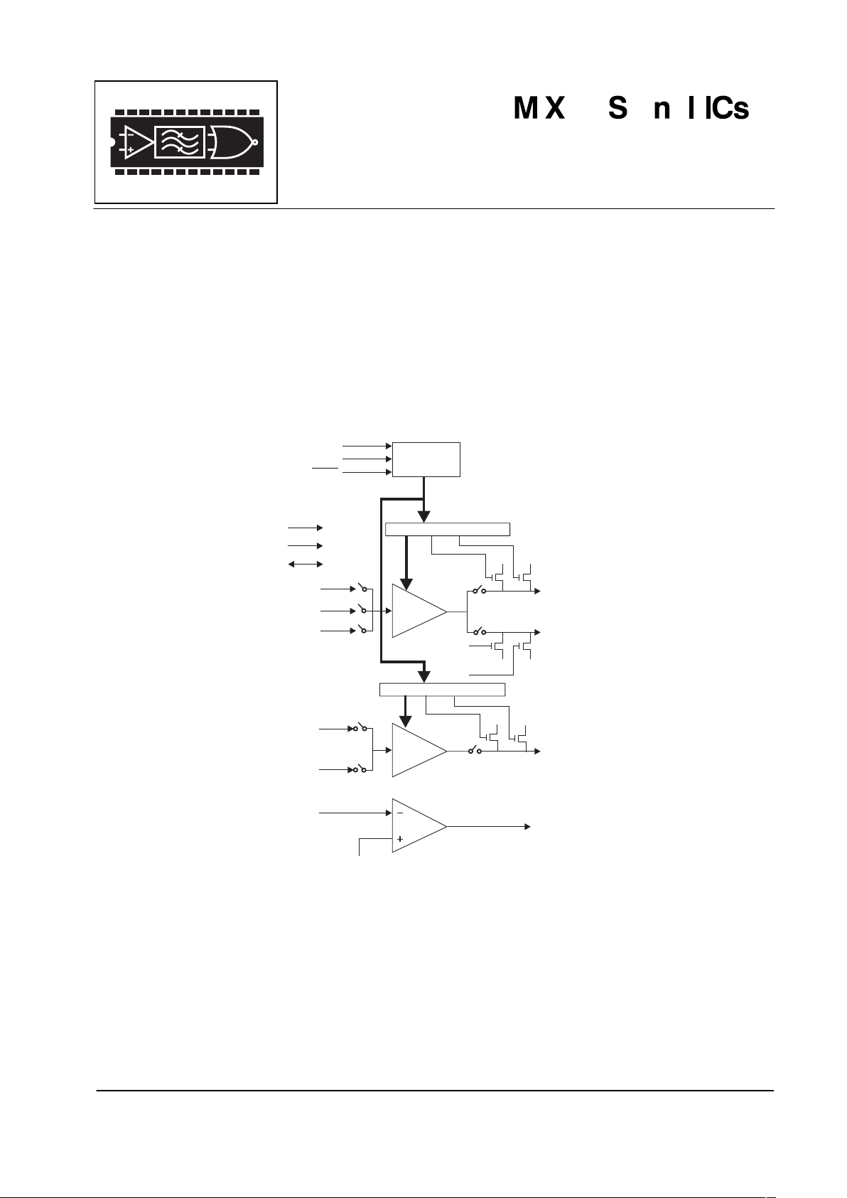
The MX029 Digitally Controlled Amplifier Array replaces audio level controls in radio and wireline
communications applications. It is a single-chip LSI circuit comprised of two discrete, digitally controlled gain
sections. Each section has 48 distinct gain steps (+/-48dB of range in 2dB steps) plus MUTE.
As shown in Figure 1, both gain stages have switchable inputs. This switching allows for selection of three
different input signals on one channel and two on the other channel. One of the channels also has output
switching. In addition to two digitally controlled gain stages, there is a general purpose inverting amplifier.
The gain of this amplifier is controlled externally via negative feedback. Control of each gain control section is
accomplished through the serial interface. All switching is accomplished using controlled rise and fall times,
thereby assuring no transients (clicks or pops).
The MX029 requires a single 5-volt supply and is available in the following packages: 16-pin SOIC
(MX029DW), 16-pin CDIP (MX029J), and 24-pin TSSOP (MX029TN).

Dual Digitally Controlled Amplifier 2 MX029
1998 MX-COM, INC. www.mxcom.com Tele: 800 638 5577 910 744 5050 Fax: 910 744 5054 Doc. # 20480096.008
4800 Bethania Station Road, Winston-Salem, NC 27105-1201 USA. All trademarks and service marks are held by their respective companies.
CONTENTS
Section Page
1. Block Diagram.................................................................................................................3
2. Signal List........................................................................................................................4
3. External Components.....................................................................................................5
4. Application.......................................................................................................................5
4.1 Recommendations ................................................................................................................. 5
5. Control Data and Timing.................................................................................................6
6. Performance Specification.............................................................................................8
6.1 Electrical Performance........................................................................................................... 8
6.1.1 Absolute Maximum Ratings..........................................................................................................8
6.1.2 Operating Limits............................................................................................................................8
6.1.3 Operating Characteristics .............................................................................................................9
6.2 Serial Interface Timing ......................................................................................................... 10
6.3 Packaging............................................................................................................................. 11
MX-COM, Inc. reserves the right to change specifications at any time and without notice.
Dual Digitally Controlled Amplifier 3 MX029
1998 MX-COM, INC. www.mxcom.com Tele: 800 638 5577 910 744 5050 Fax: 910 744 5054 Doc. # 20480096.008
4800 Bethania Station Road, Winston-Salem, NC 27105-1201 USA. All trademarks and service marks are held by their respective companies.
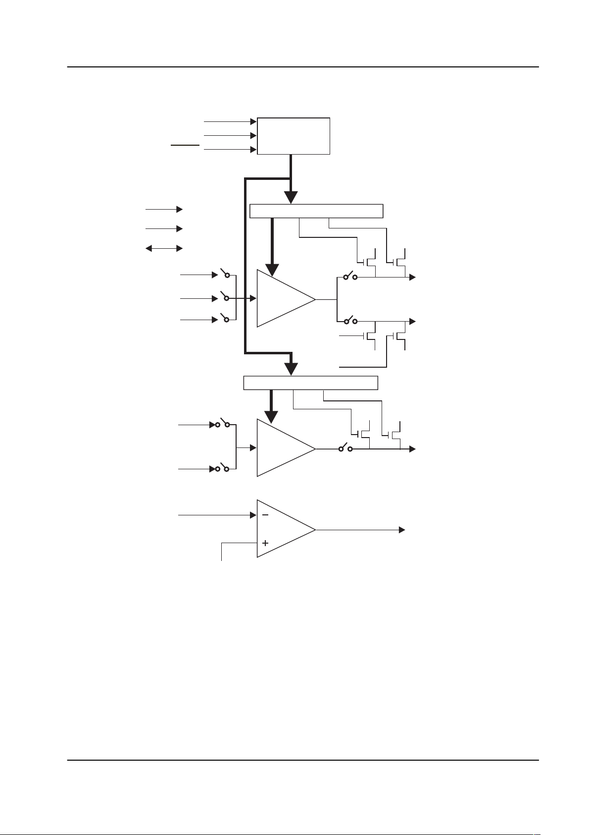
1. Block Diagram
LOAD/LATCH
DATA IN PUT
SERIAL CLOCK
SERIAL
INTERFACE
∆
G
∆
G
CH1, OUTPUT 1
STAGE 1 CONTROL REGISTER
STAGE 1 CONTROL REGISTER
TO STAGE 1
CONTROL
REGISTER
CH1, OUTPUT 2
CH2, OUTPUT 1
CH2, INPUT 2
CH2, INPUT 1
CH1, INPUT 3
CH1, INPUT 2
CH1, INPUT 1
BIAS
BIAS
BIAS
BIAS
BIAS
V
SS
V
SS
V
SS
V
SS
V
DD
UNIVERSAL
AMP OUT
UNIVERSAL
AMP IN
Figure 1: Device Block Diagram
Dual Digitally Controlled Amplifier 4 MX029
1998 MX-COM, INC. www.mxcom.com Tele: 800 638 5577 910 744 5050 Fax: 910 744 5054 Doc. # 20480096.008
4800 Bethania Station Road, Winston-Salem, NC 27105-1201 USA. All trademarks and service marks are held by their respective companies.
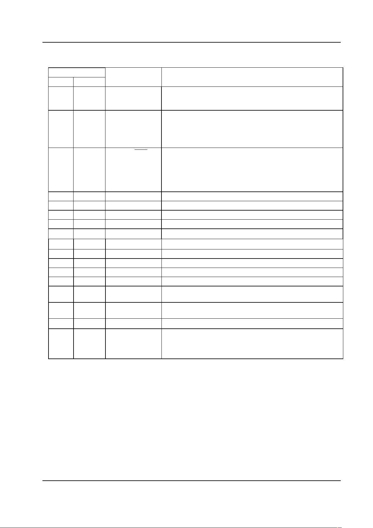
2. Signal List
Pin No. Type Description
J, DW TN
1 1 Serial Clock This external clock input is used to “clock in” the Control Data.
See Figure 4 for timing information. This input has an internal
1M pullup resistor.
2 4 Control (Data) Input: Operation of the two amplifier channels (Ch1 - Ch2) is
controlled by the data entered serially at this pin. The data is
entered (bit 13 to bit 0) on the rising edge of the external Serial
Clock. The data format is described in Tables 1-5 and Figure 3.
This input has an internal 1M pullup resistor.
35
Load/
Latch
This function governs the loading and execution of the control
data. During serial data loading this input should be kept at a
logical “1” to ensure that data rippling past the latches has no
effect. When all 14 bits have been loaded this input should be
strobed “1 - 0 -1” to latch the new data in. Data is executed on
the rising edge of the strobe.
4 6 Ch 1 Input 1 Analog Input.
5 7 Ch 1 Input 2 Analog Input.
6 8 Ch 2 Input 1 Analog Input.
7 9 Ch 2 Input 2 Analog Input.
812 VSSNegative supply (GND).
913 V
BIAS
The output of the on-chip bias circuitry, held at VDD/2.
10 16 Ch 1 Input 3 Analog Input. Normally used for FSK data.
11 17 Ch 2 Output Analog Output.
12 18 Ch 1 Output Analog Output.
13 20 Ch 1 Output Analog Output.
14 21 Universal
Amp Out
Output from general purpose amplifier.
15 23 Universal
Amp In
Inverting input to general purpose amplifier.
16 24 V
DD
Positive supply rail. A single +5-volt power supply is required.
2, 3, 10,
11,14,
15, 19,
22
N/C No internal connection
 Loading...