COMMUNICATION SEMICONDUCTORS
CMX838
DATA BULLETIN
FRS/PMR446/GMRS
Family Radio Processor
¤
¤¤
¤2001 MX-COM, Inc. www.mxcom.com Tel: 800 638 5577 336 744 5050 Fax: 336 744 5054 Doc. # 20480221.002
4800 Bethania Station Road, Winston-Salem, NC 27105-1201 USA All trademarks and service mark s are held by their res pec t ive companies.
ADVANCE INFORMATION
Features and Applications
• Advanced one-of-any CTCSS
subaudio 50 tone processor
• Fast decode time
• IRQ on any / all valid tones
• Fast scan, group calling, auto
response tone select and
Tone Cloning™ support
• Supply Independent output level
• RF Synthesizer
• FRS, PMR446 and GMRS RF
channels
• Configurable charge pump
• Audio call tone generator
• Audio processing
• Mic amplifier
• Pre/Deemphasis
• Limiter with Supply Independent
output level
• Post limiter filtering
• Mic, Rx and Tx digital gain controls
• Single and dual Tx outputs
• Signal source and external function
switches
• Low power, 3V t o 5V suppl y
• Powersave and sleep modes
• Serial control interface
MICIN
RXIN
RXOUT
TXMOD1
XTAL
AUX I/O
C-BUS
-RF
IN
+RF
IN
REF
IN
SV
SS
SV
DD
XTAL
XTAL
I
SET
CP
OUT
RF SYNTHESIZER
S
TXMOD2
MICOUT
TIMING
GENERATION
IRQ
RPLY DATA
CMD DATA
SERIAL CLOCK
CS
PROGRAMMABLE SUB-
AUDIO PROCESSOR
MODULATION OUTPUT
SELECT AND LEVEL
CONTROL
AUDIO PROCESSOR
BIAS
V
BIAS
V
SS
V
DD
A
GENERAL PURPOSE
TIMER AND TONE
GENERATOR
The highly integrated CMX838 Family Radio Processor includes subaudio, audio, and synthesizer functions
to serve as the core engine for low cost, high performance FRS, PMR446, and GMRS radio designs. Its
flexibility supports both simple and advanced multi-channel radios without cost penalties. Integrated Tx
voltage reference and baseband clock generation circuits eliminate the need for external components. The
CMX838’s features directly supports advanced end product functions such as: group calling, scanning,
automatic scanner response tone setup, and Tone Cloning™.
By using the CMX838 one global radio design can support multiple standards and markets.
Controlled via a serial interface (C-BUS) the Family Radio Processor operates from a 3V to 5V supply and is
available in 28-pin TSSOP (CMX838E1) and 28-pin SOIC (CMX838D1) packages.

FRS/PMR446/GMRS Family Radio Processor 2 CMX838 Advance Information
¤
¤¤
¤2001 MX-COM, Inc. www.mxcom.com Tel: 800 638 5577 336 744 5050 Fax: 336 744 5054 Doc. # 20480221.002
4800 Bethania Station Road, Winston-Salem, NC 27105-1201 USA All trademarks and service mark s are held by their res pec t ive companies.
CONTENTS
Section Page
1 Block Diagram............................................................................................................... 7
2 Signal List...................................................................................................................... 8
3 External Components................................................................................................. 10
4 General Description....................................................................................................11
4.1 Audio ...............................................................................................................................11
4.1.1 Digitally Controlled Amplifiers (DCA).................................................................................... 11
4.1.2 Transmit Input Amplifier........................................................................................................12
4.1.3 Audio Switched Capacitor Filters.......................................................................................... 12
4.1.3.1 Preemphasis/Low-pass Filter......................................................................................... 13
4.1.3.2 High-pass Filter ..............................................................................................................14
4.1.3.3 Deviation Limiter Low-pass Filter................................................................................... 14
4.1.4 Deemphasis.......................................................................................................................... 15
4.1.5 Transmit Audio Path .............................................................................................................15
4.1.6 Rec ei ve Audio Path ..............................................................................................................16
4.1.7 Aud io Pat h witho ut Deemphasis or Preemphasis ................................................................ 16
4.1.8 Deviation Limiter................................................................................................................... 17
4.2 Tone Signaling Processor................................................................................................18
4.2.1 Tone encoding/decoding ...................................................................................................... 18
4.2.2 Subaudio RX and TX Filter Characteristics.......................................................................... 19
4.2.3 CTCSS Subaudio Decoder and Encoder Tone Set.............................................................. 21
4.2.4 Tone Signaling Processor Configuration Task Descriptions ................................................ 22
4.2.4.1 Normal Run Mode (Task 0)............................................................................................22
4.2.4.2 Reserved For Test (Task 1-3) ........................................................................................ 22
4.2.4.3 RX Configuration ............................................................................................................ 23
4.2.4.4 TX Configuration............................................................................................................. 24
4.2.4.5 Initialize and Configure................................................................................................... 24
4.3 RF Synthesizer ................................................................................................................ 27
4.3.1 Operating Range and Specifications.................................................................................... 27
4.3.2 Main Divider.......................................................................................................................... 27
4.3.3 Phas e Detec t or & Charge Pump .......................................................................................... 27
4.3.4 Lock Detect Output............................................................................................................... 28
4.3.5 Reference Circuits ................................................................................................................ 28
4.4 Baseband Timing Generation ..........................................................................................28

FRS/PMR446/GMRS Family Radio Processor 3 CMX838 Advance Information
¤
¤¤
¤2001 MX-COM, Inc. www.mxcom.com Tel: 800 638 5577 336 744 5050 Fax: 336 744 5054 Doc. # 20480221.002
4800 Bethania Station Road, Winston-Salem, NC 27105-1201 USA All trademarks and service mark s are held by their res pec t ive companies.
5 Software Programming............................................................................................... 29
5.1 C-BUS Serial Interface.....................................................................................................29
5.1.1 8-Bit C-BUS Register Map.................................................................................................... 30
5.1.2 16-Bit C-BUS Register Map.................................................................................................. 31
5.1.2.1 GENERAL RESET ($01)................................................................................................31
5.1.2.2 SETUP Register ($80).................................................................................................... 32
5.1.2.3 AUDIO CONTROL Register ($81).................................................................................. 33
5.1.2.4 RX AUDIO LEVEL CONTROL Register ($82) ............................................................... 34
5.1.2.5 AUDIO POWER AND BANDWIDTH CONTROL Register ($83) ................................... 35
5.1.2.6 TXMOD 1 & 2 CONTROL Register ($88)....................................................................... 36
5.1.2.7 SYNTHESIZER BASEBAND CLK CONTROL Register ($89)....................................... 38
5.1.2.8 SYNTHESIZER GENERAL CONTROL Register ($8A)................................................. 39
5.1.2.9 SYNTHESIZER CHANNEL SELECT Register ($8B)..................................................... 40
5.1.2.10 SYNTHESIZER STATUS Register ($8C)....................................................................... 40
5.1.2.11 SYNTHESIZER 1ST IF OFFSET Register ($8D)........................................................... 41
5.1.2.12 16 BIT SUBAUDIO TASK DATA Register ($8E)............................................................ 41
5.1.2.13 16 BIT SUBAUDIO TEST DATA Register ($8F) ............................................................ 41
5.1.2.14 SYNTHESIZER TEST Register ($90) ............................................................................ 41
5.1.2.15 16 BIT SUBAUDIO TEST READ DATA Register ($91) ................................................. 42
5.1.2.16 SUBAUDIO PROCESSOR GENERAL CONTROL Register ($93)................................ 42
5.1.2.17 SUBAUDIO STATUS Register ($94).............................................................................. 43
5.1.2.18 SUBAUDIO TASK 8 BIT DATA Register ($95).............................................................. 43
5.1.2.19 SUBAUDIO ANALOG CONTROL Register ($97).......................................................... 44
6 Application Notes........................................................................................................ 46
6.1 Overview..........................................................................................................................46
6.2 Basic FRS Radio Architecture..........................................................................................47
6.3 CMX838 Architectural Overview ......................................................................................48
6.4 Detailed CMX838 Architecture......................................................................................... 48
6.4.1 Aud io Proc ess ing..................................................................................................................49
6.4.2 Tone Signaling Processor..................................................................................................... 51
6.4.3 Lev el Control......................................................................................................................... 53
6.4.4 Synthesizer and Charge Pump............................................................................................. 55
6.4.5 Clock Generation.................................................................................................................. 55
6.4.6 Powersave Functions ........................................................................................................... 56
6.5 Control Registers Illustrated.............................................................................................56
6.6 Application Examples.......................................................................................................58
6.6.1 CMX 838 Ini tia li za tion ............................................................................................................ 58
6.6.1.1 Register Descriptions: .................................................................................................... 58
6.6.2 TX, subaudio encoding, single point modulation.................................................................. 59
6.6.2.1 Register Descriptions: .................................................................................................... 59
6.6.3 RX, subaudio decode CTCSS tone or tones........................................................................61
6.6.3.1 Register Descriptions: .................................................................................................... 61
6.6.4 RX, multiple subaudio tone detect - Tone Cloning™............................................................ 63
6.6.4.1 Register Descriptions: .................................................................................................... 63

FRS/PMR446/GMRS Family Radio Processor 4 CMX838 Advance Information
¤
¤¤
¤2001 MX-COM, Inc. www.mxcom.com Tel: 800 638 5577 336 744 5050 Fax: 336 744 5054 Doc. # 20480221.002
4800 Bethania Station Road, Winston-Salem, NC 27105-1201 USA All trademarks and service mark s are held by their res pec t ive companies.
7 Performance Specification......................................................................................... 65
7.1 Electrical Performance ..................................................................................................... 65
7.1.1 Abs ol ute Maximum Ratings.................................................................................................. 65
7.1.2 Operating Limits....................................................................................................................65
7.1.3 Operating Characteristics ..................................................................................................... 66
7.1.4 Timing................................................................................................................................... 69
7.2 Packaging........................................................................................................................70
MX-COM, Inc. reserves the right to change specifications at any time and without notice.

FRS/PMR446/GMRS Family Radio Processor 5 CMX838 Advance Information
¤
¤¤
¤2001 MX-COM, Inc. www.mxcom.com Tel: 800 638 5577 336 744 5050 Fax: 336 744 5054 Doc. # 20480221.002
4800 Bethania Station Road, Winston-Salem, NC 27105-1201 USA All trademarks and service mark s are held by their res pec t ive companies.
FIGURES
Figure Page
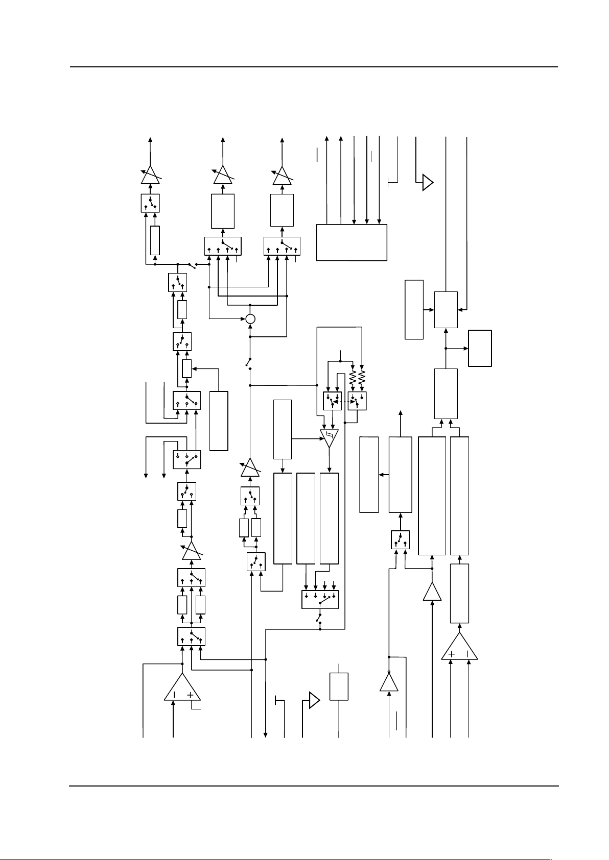
Figure 1: Block Diagram.....................................................................................................................................7
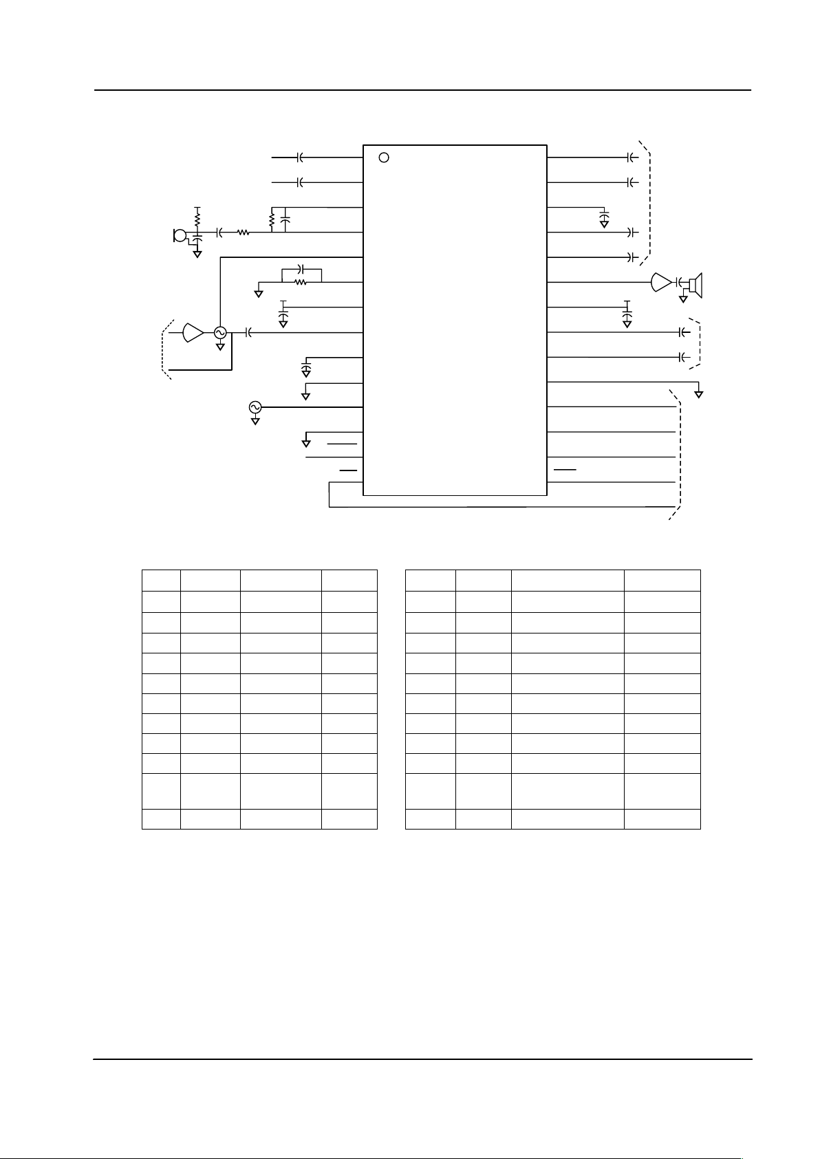
Figure 2: Recommended External Components..............................................................................................10
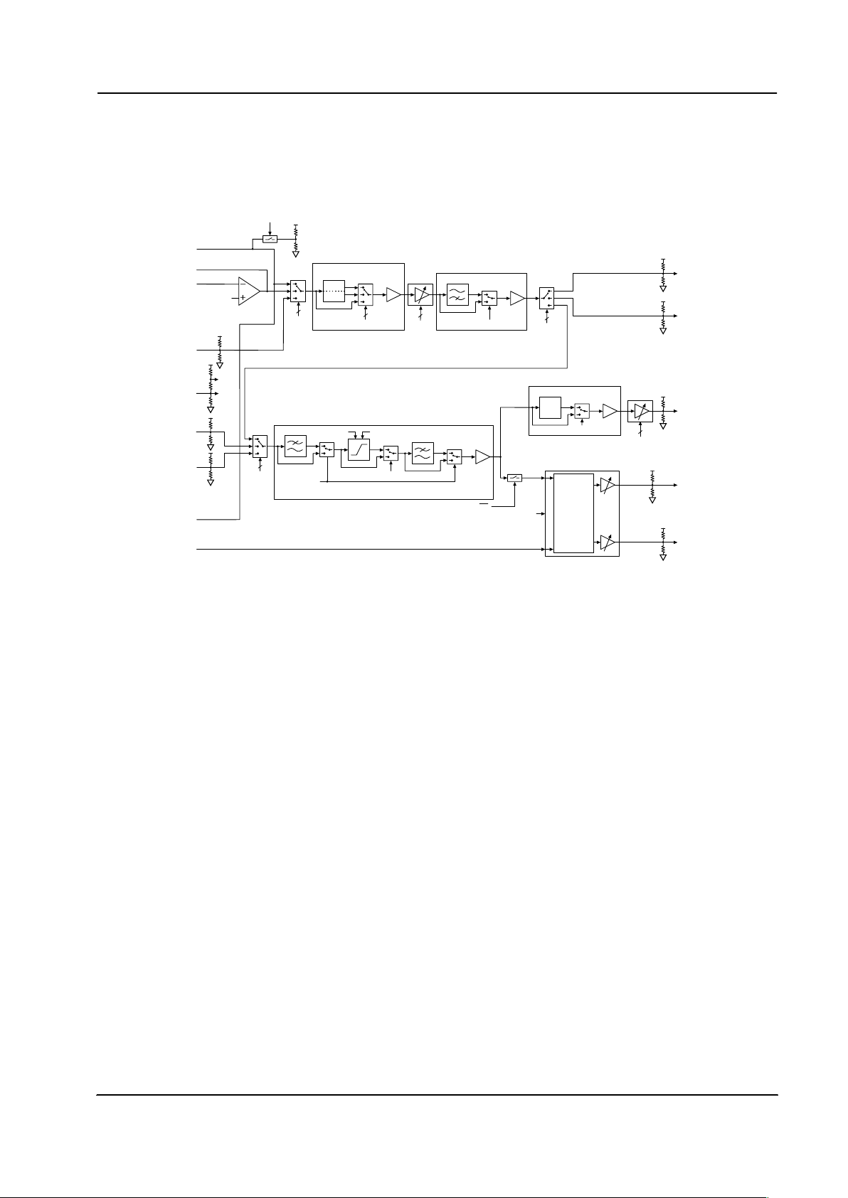
Figure 3: Audio Processing Block Diagram......................................................................................................11
Figure 4: Digitally controlled amplifiers and switch matrix for adjusting and switching transmit audio and
subaudio signals. ..............................................................................................................................12
Figure 5: TX Input Amplifier.............................................................................................................................. 12
Figure 6: Magnitude response for input low-pass filter. ................................................................................... 13
Figure 7: Magnitude response for preemphasis filter.......................................................................................13
Figure 8: Magnitude response of high-pass filter.............................................................................................14
Figure 9: Magnitude response of post-deviation limiter low-pass filter. ........................................................... 14
Figure 10: Magnitude response of deemphasis filter.......................................................................................15
Figure 11: Transmit audio path frequency response with preemphasis. ......................................................... 15
Figure 12: Receive audio path frequency response with deemphasis.............................................................16
Figure 13: Audio path frequency response without preemphasis or deemphasis. .......................................... 16
Figure 14: Deviation limiter block diagram . ......................................................................................................17
Figure 15: Subaudio Block Diagram.................................................................................................................18
Figure 16: Subaudio RX filter gain for normal CTCSS operation.....................................................................19
Figure 17: Subaudio RX filter delay for normal CTCSS operation................................................................... 19
Figure 18: Subaudio TX level for normal CTCSS operation (Magnitude scale with respect to 0dBV) ............20
Figure 19: Subaudio TX filter delay for normal CTCSS operation. ..................................................................20
Figure 20: RF Synthesizer block diagram........................................................................................................27
Figure 21: Block diagram of main programmable divider.................................................................................27
Figure 22: C-BUS transaction timing diagram..................................................................................................29
Figure 23: Basic FRS Radio Tx Architecture ................................................................................................... 47
Figure 24: Basic FRS Radio Rx Architecture...................................................................................................47
Figure 25: CMX838 Main Function Blocks....................................................................................................... 48
Figure 26: CMX838 Main Sections................................................................................................................... 48
Figure 27: Audio Processing ............................................................................................................................ 49
Figure 28: Example Audio RX Path.................................................................................................................. 49
Figure 29: Example Audio TX Voice Path........................................................................................................50
Figure 30: Example Audio TX Internally Generated T one with Lou ds peak er Enabled Path ...........................50
Figure 31: Tone Signaling Processor...............................................................................................................51
Figure 32: Example CTCSS Tone Decoder Path.............................................................................................52
Figure 33: Example CTCSS Tone Encoder Path.............................................................................................52
Figure 34: Example Internal Audio Tone Enco der Pat h................................................................................... 53
Figure 35: Level Control...................................................................................................................................53
Figure 36: Example Single Point Modulati on Level Pat h ................................................................................. 54
Figure 37: Example Two-Point Modulation Level Paths .................................................................................. 54
Figure 38: Example Single Point Modul ation with Varied Subaudio Level Paths............................................54
Figure 39: Synthesizer and Charge Pump.......................................................................................................55
Figure 40: Clock Generation ............................................................................................................................ 55
Figure 41: Powersave Scope and Related Control Regis ters.......................................................................... 56

FRS/PMR446/GMRS Family Radio Processor 6 CMX838 Advance Information
¤
¤¤
¤2001 MX-COM, Inc. www.mxcom.com Tel: 800 638 5577 336 744 5050 Fax: 336 744 5054 Doc. # 20480221.002
4800 Bethania Station Road, Winston-Salem, NC 27105-1201 USA All trademarks and service mark s are held by their res pec t ive companies.
Figure 42: Synthesizer to Baseband Clock Control, $89 ................................................................................. 56
Figure 43: Setup, $80.......................................................................................................................................57
Figure 44: Audio ($81), RX Audio Level ($82) and Subaudio Analog ($97) Control ....................................... 57
Figure 45: Audio Power and Bandwidth Control, $83 ...................................................................................... 58
Figure 46: TXMOD1 & TXMOD2 Control, $88.................................................................................................58
Figure 47: Application Exam ple TX, Subaudio Enc od i ng, Sin gle Poi nt Modu lat ion ........................................61
Figure 48: C-BUS Timing ................................................................................................................................. 69
Figure 49: 28-pin TSSOP (E1) Mechanical Outline: Order as part no. CMX838E1 ....................................... 70
Figure 50: 28-pin SOIC (D1) Mechanical Outline: Order as part no. CMX838D1...........................................70
FRS/PMR446/GMRS Family Radio Processor 7 CMX838 Advance Information
¤
¤¤
¤2001 MX-COM, Inc. www.mxcom.com Tel: 800 638 5577 336 744 5050 Fax: 336 744 5054 Doc. # 20480221.002
4800 Bethania Station Road, Winston-Salem, NC 27105-1201 USA All trademarks and service mark s are held by their res pec t ive companies.
1 Block Diagram
CTCSS DECODERS
+
CTCSS ENCODE
RXIN
BIAS
AUX I/O
C-BUS
Serial
Interface
DIVIDE 32/33
PROGRAMMABLE DIVIDER
12 BIT PROGRAMMABLE
REFERENCE COUNTER
PHASE
DETECTOR
CHARGE
PUMP
LOCK
DETECT
+RF
I N
-RF
I N
REF
I N
SV
SS
SV
DD
V
BIAS
XTAL
XTAL
I
SET
CP
OUT
V
SS
V
DD
S
BASEBAND
TIMING GENERATION
SERIAL CLOCK
CS
LPF
V
BIAS
V
BIAS
V
BIAS
AUDIOTONE ENCODE
0°/180°
phase
0°/180°
phase
CMD DATA
RPLY DATA
IRQ
TXMOD1
TXMOD2
RX NOTONE/
TX DURATION TIMER
VOLTAGE REF
BPF
MICIN
MICOUT
PRE
LPF
HPF
LPF
LIM
B
IN
A
IN
A
OUTBOUT
V
BIAS
VOLTAGE REF
DEEMP
VOLTAGE REF
1
0
V
BIAS
RXOUT
Figure 1: Block Diagram

FRS/PMR446/GMRS Family Radio Processor 8 CMX838 Advance Information
¤
¤¤
¤2001 MX-COM, Inc. www.mxcom.com Tel: 800 638 5577 336 744 5050 Fax: 336 744 5054 Doc. # 20480221.002
4800 Bethania Station Road, Winston-Salem, NC 27105-1201 USA All trademarks and service mark s are held by their res pec t ive companies.
2 Signal List
Package Signal Description
Pin No.
E1/D1
Name Type
1 RXIN input Receive input for both audio and subaudio signals.
2 AUX I/O input/output When configured as an input this pin can be used to route
externally generated ringing or alert signals to the Rx and
Tx audio paths.
When configured as an output this pin allows for
monitoring internally generated ringing or alert signals.
See Section 4.2.4.5.3
3 MICOUT output Microphone amplifier feedback output.
4 MICIN input Microphone amplifier input. This is the inverting input to a
high gain opamp, suitable for use with common
microphones.
5 CP
OUT
output Synthesizer charge pump output. Apply to external loop
filter that drives the control input of an external VCO
6
I
SET
input Synthesizer charge pump current control. Connect via
external resistor to SV
SS
to set charge pump current.
7 SVDD power Synthesizer positive supply. This signal must be
decoupled to SV
SS
by a capacitor mounted close to the
device pins.
8 -RFIN input Synthesizer RF negative input. Connect this pin to SVSS
(synthesizer common) when a non-differential input signal
is applied to +RF
IN
.
9 +RFIN input Synthesizer RF positive input.
10 SVSS power Synthesizer negative supply.
11 REFIN input Synthesizer reference oscillator input.
12 XTAL input The input to the on-chip oscillator, for external Xtal circuit
or clock. This input should be connected to V
SS
, Circuit
Common, when the device is configured to generate the
XTAL clock internally from the REF
IN
clock.
13
XTAL
output Inverted output of the on-chip crystal oscillator. This pin
should not be connected (left open) when the device is
configured to generate the XTAL clock internally from the
REF
IN
clock.
14
CS
input C-BUS select data loading control function input. This
input controls C-BUS transfer initiation, completion and
cancellation.
15
IRQ
output Interrupt output, logic '0' active level. This is a 'wire-
Orable' output, enabling the connection of multiple
peripherals to 1 interrupt port on an external µController.
This pin has a low impedance pull-down to logic "0" when
active and a high-impedance when inactive. An external
pull-up resistor is required. Interrupt outputs may be
configured via mask bits via C-BUS commands.
16 RPLY DATA output Reply data output to C-BUS serial control port. Output
reply data bytes are synchronized to the CLK clock input
under the control of the
CS input. This 3-state output is
held at high impedance when not driving output data.
17 CMD DATA input Command data input to C-BUS serial control port. Data is
loaded into this device in 8-bit bytes, MSB (D7) first, and
LSB (D0) last, synchronized to the CLK clock input.

FRS/PMR446/GMRS Family Radio Processor 9 CMX838 Advance Information
¤
¤¤
¤2001 MX-COM, Inc. www.mxcom.com Tel: 800 638 5577 336 744 5050 Fax: 336 744 5054 Doc. # 20480221.002
4800 Bethania Station Road, Winston-Salem, NC 27105-1201 USA All trademarks and service mark s are held by their res pec t ive companies.
Package Signal Description
18 SERIAL CLOCK input Serial clock input to C-BUS serial control port. This clock
input controls transfer timing of commands and data to
and from the device.
19 VSS power Negative supply (Circuit Common)
20 TXMOD2 output Transmit Output 2 internally switch selected to be at any
of (1) V
BIAS
, (2) transmit subaudio or (3) transmit audio
summed with subaudio.
21 TXMOD1 output Transmit Output 1 internally switch selected to be at any
of (1) V
BIAS
, (2) transmit audio or (3) transmit audio
summed with subaudio.
22 VDD supply Positive supply. Levels and voltages are dependent upon
this supply. This signal must be decoupled to V
SS
by a
capacitor mounted close to the device pins.
23 RXOUT output Processed receive audio output.
24 BIN input External processing Path B input.
25 AIN input External processing Path A input.
26 V
BIAS
bi-directional A bias line for the internal circuitry, driven to VDD/2 by a
high impedance source. This signal must be decoupled by
a capacitor mounted close to the device pins.
27 B
OUT
output External processing Path B output. This provides internal
switch controlled access to either Rx or Tx audio signals
for external processing such as expanding and
unscrambling.
28 A
OUT
output External processing Path A output. This provides internal
switch controlled access to either Rx or Tx audio signals
for external processing such as compressing and
scrambling.
Table 1: Signal List
FRS/PMR446/GMRS Family Radio Processor 10 CMX838 Advance Information
¤
¤¤
¤2001 MX-COM, Inc. www.mxcom.com Tel: 800 638 5577 336 744 5050 Fax: 336 744 5054 Doc. # 20480221.002
4800 Bethania Station Road, Winston-Salem, NC 27105-1201 USA All trademarks and service mark s are held by their res pec t ive companies.
3 External Components
A
OUT
B
OUT
V
BIAS
A
IN
B
IN
RXOUT
V
DD
TXMOD1
TXMOD2
RXIN
IRQ
RPLY DATA
CMD DATA
SERIAL CLOCK
V
SS
CMX838E1
AUX I/O
MICOUT
MICIN
CP
OUT
I
SET
SV
DD
REF
IN
-RF
IN
+RF
IN
SV
SS
XTAL
XTAL
CS
C-BUS
Serial
Control
Interface
C1
C2
C3
C4
C5
C6
C7
C8
C15
C14
C13
C12
C11
C10
C9
U2
RF
Section
REF
OSC
VCO
From RF Receiver
FromTone Generator
Microphone
RF
Section
R1
R2
R4
R3
1
2
3
4
5
6
7
8
9
10
11
12
13
14
28
27
26
25
24
23
22
21
20
19
18
17
16
15
C16
Optional
External
Audio
Processing
Figure 2: Recommended External Components
R1 Note 1
470k
Ω
±5% C9 0.1µF ±20%
R2 Note 1
10k
Ω
±5% C10 0.1µF ±20%
R3 Note 2
100k
Ω
±10% C11 0.1µF ±20%
R4 Note 3 ±10% C12 0.1µF ±20%
C1 0.1µF ±20% C13 0.1µF ±20%
C2 0.1µF ±20% C14 0.1µF ±20%
C3 Note 1 33pF ±20% C15 0.1µF ±20%
C4 Note 1 0.1µF ±20% C16 47.0pF ±20%
C5 Note 2 0.1µF ±20%
C6 0.1µF ±20%
C7 0.1µF ±20% U2 Speaker driver
e.g. LM386
C8 0.1µF ±20%
External Components Notes:
1. R1, R2, C3 and C4 form the gain components for the Tx Input Amplifier (microphone amplifier). R1
should be chosen as required by the signal level, using the following formula:
Gain = -R1/R2
C3 x R1 should be chosen so as not to compromise the high frequency performance and C4 x R2
should be chosen so as not to compromise the low frequency performance.
2. R3 and C5 values are dependent on microphone specifications.
3. R4 Sets charge pump source current. The value of R4 can vary between about 50k
Ω and 250kΩ. This
gives a charge pump current range of 0.8mA to 8.4mA
FRS/PMR446/GMRS Family Radio Processor 11 CMX838 Advance Information
¤
¤¤
¤2001 MX-COM, Inc. www.mxcom.com Tel: 800 638 5577 336 744 5050 Fax: 336 744 5054 Doc. # 20480221.002
4800 Bethania Station Road, Winston-Salem, NC 27105-1201 USA All trademarks and service mark s are held by their res pec t ive companies.
4 General Description
4.1 Audio
The audio signal processing is designed to meet or exceed the requirements for basic audio filtering, gain
control and deviation limiting in a FRS radio. Figure 3 is a block diagram of the audio circuitry.
RXIN
TX SUBAUDIO (From On-Chip SubaudioTone Generator)
RXOUT
AUX I/O
MICIN
MICOUT
V
REF
LP
PRE
1
1
1
DE
1
TXMOD1
A
OUT
B
OUT
A
IN
B
IN
DEEMPHASIS NETWORK
DEVIATION LIMITER AND POST-LIMITER LPF
PREEMPHASIS OR 2
ORDER LPF
ND
6 ORDER HPF
TH
LPF BYPASS
LIMITER BYPASS
AUDIO
INPUT 1
SELECT
AUDIO OUT
SELECT
PRE LPF CTRL HPF BYPASS
DEBP
RX AUDIO OUT
LEVEL
AUDIO
LEVEL
V
REF
V
BIAS
TOS
VLHVLL
TOS
TXMOD2
TX/RX
TONE GENERATOR
AUXPUPEN
AUDIO
INPUT 2
SELECT
TXMOD
SWITCH
MATRIX and
PHASE
CONTROL
See Figure 4
Figure 3: Audio Processing Block Diagram
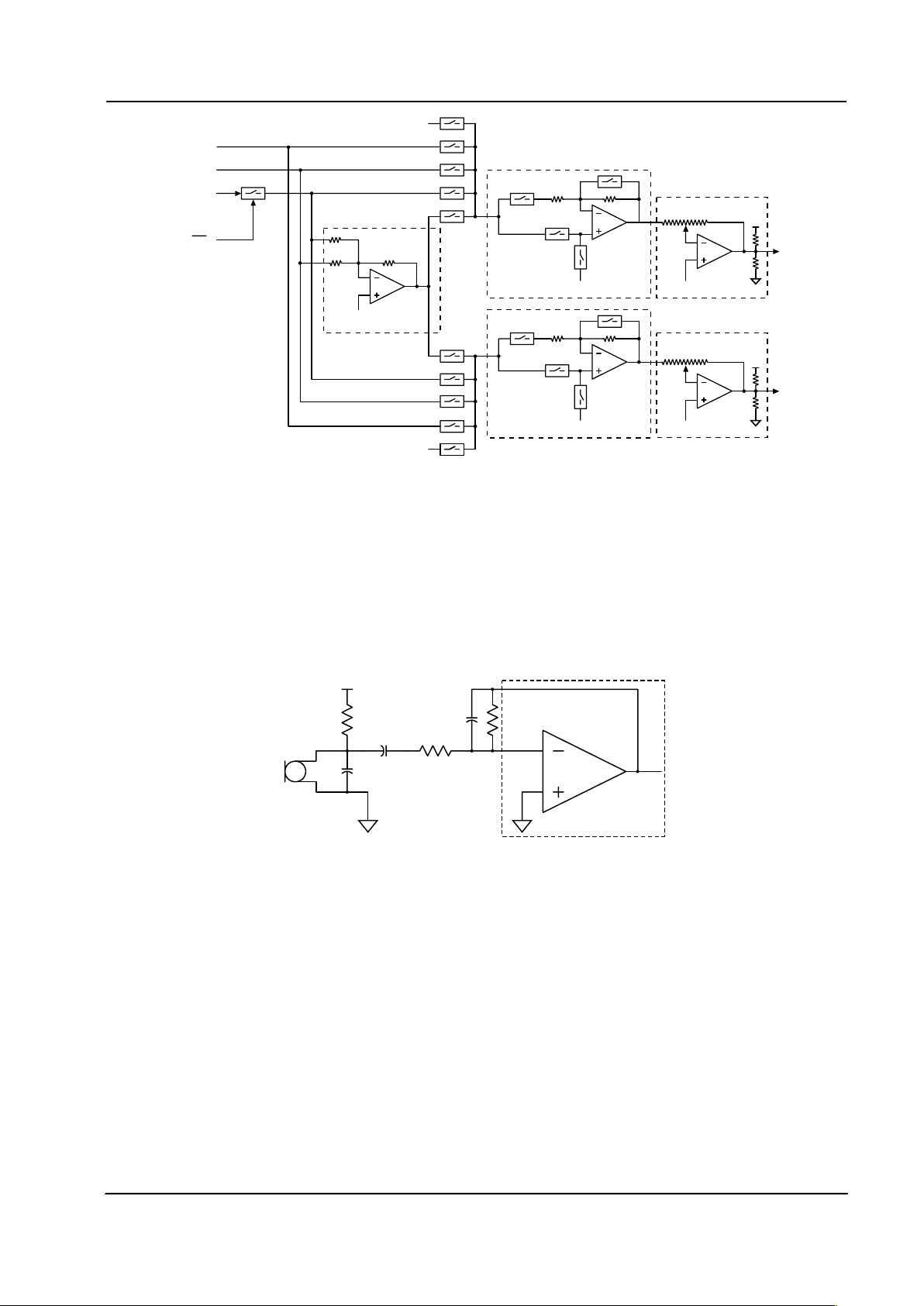
4.1.1 Digitally Controlled Amplifiers (DCA )
There are five DCAs on-chip. They are used to set signal levels for audio in/out, subaudio in/out, receive
audio out (volume control), modulation out1, and modulation out2. The audio in/out DCA is adjustable in
0.5dB steps over a +7.5dB to –7.5dB range, see Section 5.1.2.3.
The volume control level DCA is adjustable
in 1.5dB steps over a +12dB to –33dB range, see Section 5.1.2.4. The subaudio signal level in/out DCA is
adjustable in 0.5dB steps over a +7.5dB to –7.5dB range, see Section 5.1.2.19
The modulation level controls are composed of two DCAs, and a switch matrix, see Figure 4. Each
modulation level DCA, modulation out1 and modulation out2, can be switched to select either the output of
the audio processor, or the output of the tone generator, or the addition of the audio and tone. In addition,
there is an internally generated DC volume (labeled ‘TOS’ in Figure 4), which can be sent to the MOD1 and
MOD2 DCA’s. This signal is not generally applicable to FRS radios. However, in some cases it may be
desirable for testing or signal generation. The modulation out1 DCA is adjustable in 0.5dB steps over a
+7.5dB to –7.5dB range and the Modulation Out2 DCA is adjustable in 0.25dB steps over a +3.75dB to
-3.75dB range, see Section 5.1.2.6. To obtain inverse signals of mod 1and mod 2, the MSB from the first byte
(bit 7) and the MSB from second byte (bit 15) have to set to logic 1, see Section 5.1.2.6.
FRS/PMR446/GMRS Family Radio Processor 12 CMX838 Advance Information
¤
¤¤
¤2001 MX-COM, Inc. www.mxcom.com Tel: 800 638 5577 336 744 5050 Fax: 336 744 5054 Doc. # 20480221.002
4800 Bethania Station Road, Winston-Salem, NC 27105-1201 USA All trademarks and service mark s are held by their res pec t ive companies.
TXMOD1
TXMOD2
V
BIAS
V
BIAS
V
BIAS
V
BIAS
V
BIAS
V
BIAS
TOS
SUBAUDIOTONE IN
LOW R
LOW R
LOW R
LOW R
LOW R
LOW R
LOW R
LOW R
SUM
Gain/Attenuation
Gain = +/-1
TX/RX
V
BIAS
Gain/Attenuation
Gain = +/-1
AUDIO IN
Figure 4: Digitally controlled amplifiers and switch matrix for adjusting and switching transmit audio
and subaudio signals.
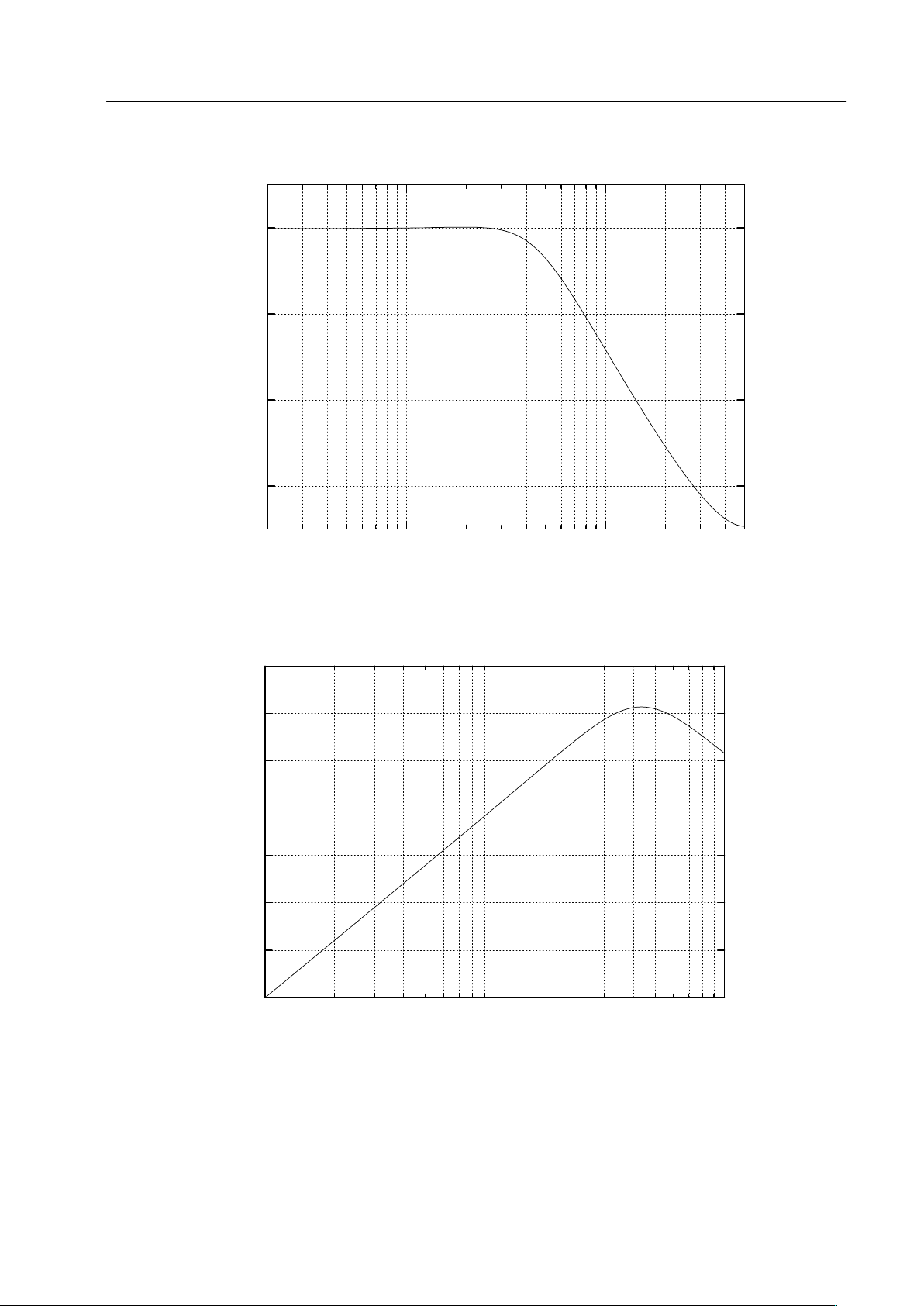
4.1.2 Transmit Input Amplifier
The transmit input amplifier is a high gain low-noise operational amplifier. Figure 5 is a simplified schematic
showing the external components required for typical application with an electret condenser microphone. The
external component values should be selected such that the feedback resistor will be greater than 10k
Ω and
the minimum gain should be greater than 6dB.
In some cases, it may be desirable to implement a pre-emphasis characteristic of appropriately configuring
the external component values around the TX input amplifier. In this case, the internal preemphasis should be
bypassed (via C-BUS).
Figure 5: TX Input Amplifier
4.1.3 Audio Switched Capacitor Filters
Four standard (composed of biquadratic sections) switched capacitor filters are used in the audio section. A
preemphasis filter (+6dB per octave from 300 to 3000 Hz intended for transmit only) is implemented using
2
nd
order switched capacitor network, which can be configured (via C-BUS) to be a 2nd order low-pass. A
6
th
order high-pass filter is used to remove subaudible tones and bandwidth limit the incoming receive or
transmit audio signal prior to being input to the limiter. A 4
th
order low-pass filter follows the deviation limiter.
This filter smoothes the transients generated by the deviation limiter. Finally, a deemphasis filter (-6dB per
octave from 300 to 3000 Hz intended for receive only) is implemented using a 2
nd
order switched capacitor
network. See Section 5.1.2 for details on configuring audio filters.
FRS/PMR446/GMRS Family Radio Processor 13 CMX838 Advance Information
¤
¤¤
¤2001 MX-COM, Inc. www.mxcom.com Tel: 800 638 5577 336 744 5050 Fax: 336 744 5054 Doc. # 20480221.002
4800 Bethania Station Road, Winston-Salem, NC 27105-1201 USA All trademarks and service mark s are held by their res pec t ive companies.
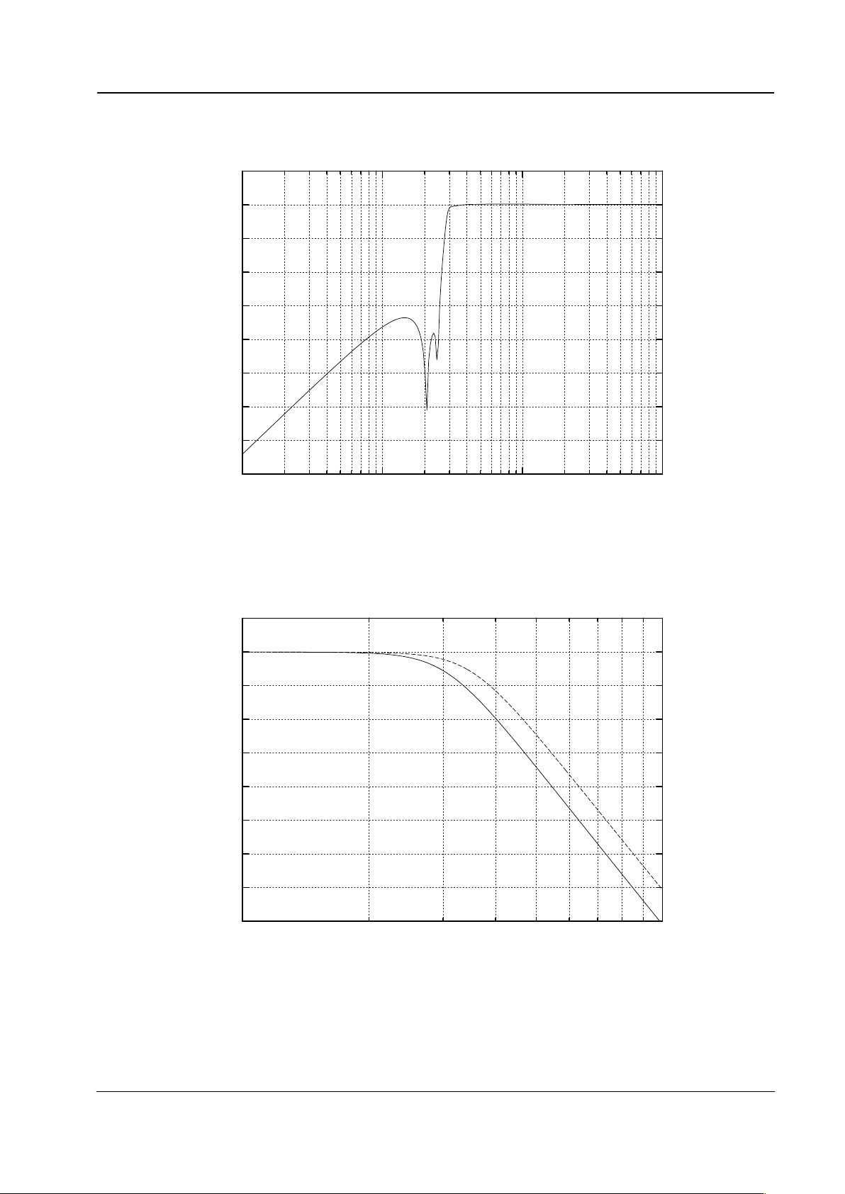
4.1.3.1 Preemphasis/Low-pass Filter
Figure 6 shows magnitude response for the Input Preemphasis/Low-pass Filter when programmed for lowpass mode. This mode would typically be selected when processing Rx audio.
-35
-30
-25
-20
-15
-10
-5
0
5
1000 10000
Magnitude (dB)
Frequency (Hz)
Figure 6: Magnitude response for input low-pass filter.
Figure 7 shows magnitude response for the Input Preemphasis/Low-pass Filter when programmed for
Preemphasis mode. This mode would typically be selected when processing Tx audio.
-20
-15
-10
-5
0
5
10
15
100 1000 10000
Magnitude (dB)
Frequency (Hz)
Figure 7: Magnitude response for preemphasis filter.
FRS/PMR446/GMRS Family Radio Processor 14 CMX838 Advance Information
¤
¤¤
¤2001 MX-COM, Inc. www.mxcom.com Tel: 800 638 5577 336 744 5050 Fax: 336 744 5054 Doc. # 20480221.002
4800 Bethania Station Road, Winston-Salem, NC 27105-1201 USA All trademarks and service mark s are held by their res pec t ive companies.
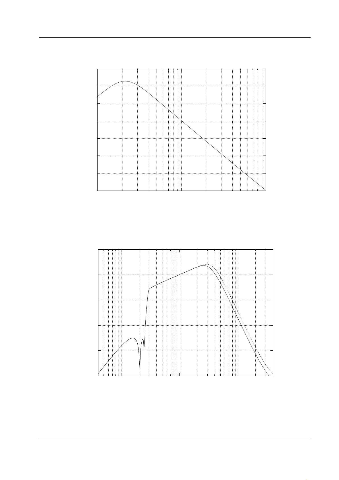
4.1.3.2 High-pass Filter
Figure 8 shows the magnitude response for the Audio High Pass Filter. This filter’s purpose is to suppress
subaudio tones when processing both Rx and Tx audio.
-80
-70
-60
-50
-40
-30
-20
-10
0
10
10 100 1000 10000
Magnitude (dB)
Frequency (Hz)
Figure 8: Magnitude response of high-pass filter.
4.1.3.3 Deviation Limiter Low-pass Filter
The magnitude response for narrowband and wideband modes is shown in Figure 9. Narrow-band mode is
generally required for transmitting in systems having RF Channel BW
≤12.5kHz (e.g. FRS).
-40
-35
-30
-25
-20
-15
-10
-5
0
5
1000 10000
Magnitude (dB)
Frequency (Hz)
WIDE BAND
NARROW BAND
Figure 9: Magnitude response of post-deviation limiter low-pass filter.
FRS/PMR446/GMRS Family Radio Processor 15 CMX838 Advance Information
¤
¤¤
¤2001 MX-COM, Inc. www.mxcom.com Tel: 800 638 5577 336 744 5050 Fax: 336 744 5054 Doc. # 20480221.002
4800 Bethania Station Road, Winston-Salem, NC 27105-1201 USA All trademarks and service mark s are held by their res pec t ive companies.
4.1.4 Deemphasis
Figure 10 shows magnitude response for the Deemphasis Filter. This filter precedes the Rx Audio Level
Control and is generally required to process Rx audio.
-20
-15
-10
-5
0
5
10
15
100 1000 10000
Magnitude (dB)
Frequency (Hz)
Figure 10: Magnitude response of deemphasis filter.
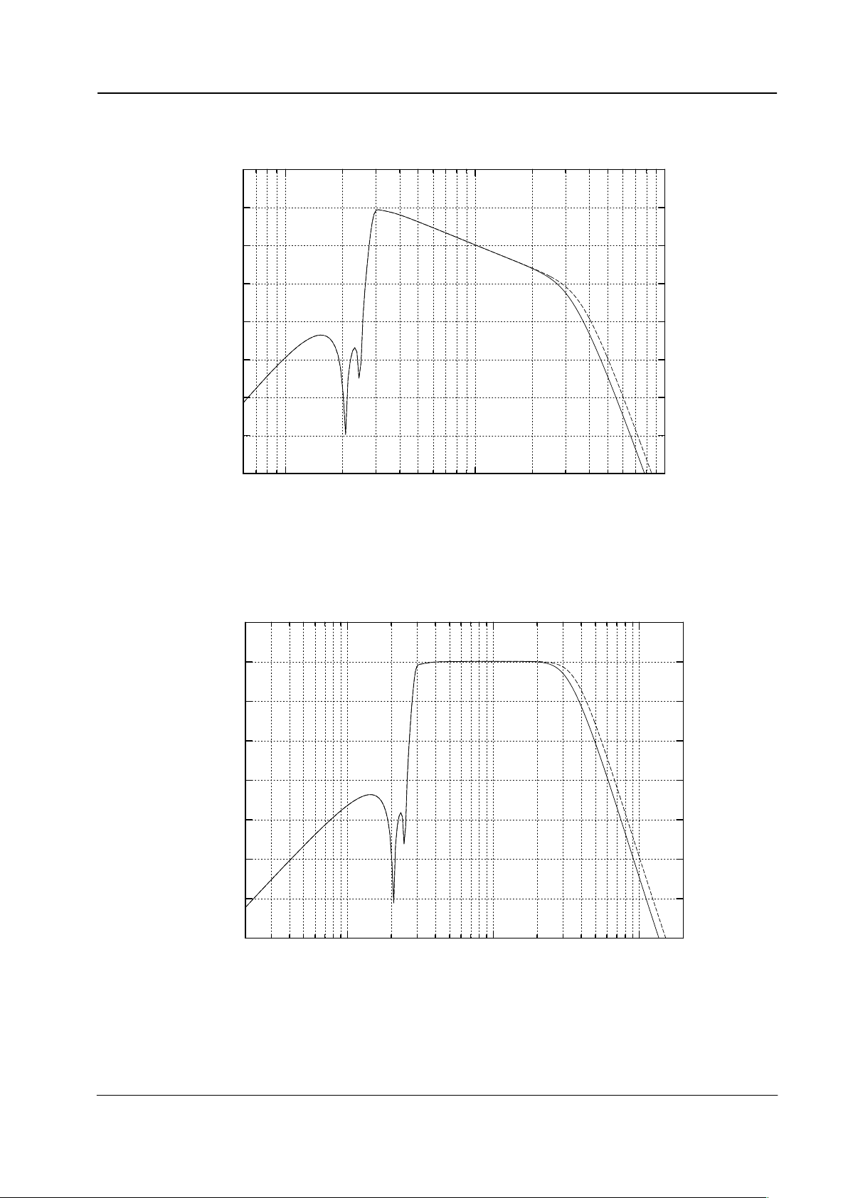
4.1.5 Transmit Audio Path
Overall magnitude response for the transmit audio path for wideband and narrowband with preemphasis is
shown in Figure 11.
-80
-60
-40
-20
0
20
100 1000 10000
Magnitude (dB)
Frequency (Hz)
NARROW BAND
WIDE BAND
Figure 11: Transmit audio path frequency response with preemphasis.
FRS/PMR446/GMRS Family Radio Processor 16 CMX838 Advance Information
¤
¤¤
¤2001 MX-COM, Inc. www.mxcom.com Tel: 800 638 5577 336 744 5050 Fax: 336 744 5054 Doc. # 20480221.002
4800 Bethania Station Road, Winston-Salem, NC 27105-1201 USA All trademarks and service mark s are held by their res pec t ive companies.
4.1.6 Receive Audio Path
Overall magnitude response for the receive audio path for wideband and narrowband with deemphasis is
shown in Figure 12.
-60
-50
-40
-30
-20
-10
0
10
20
100 1000 10000
Magnitude (dB)
Frequency (Hz)
NARROW BAND
WIDE BAND
Figure 12: Receive audio path frequency response with deemphasis.
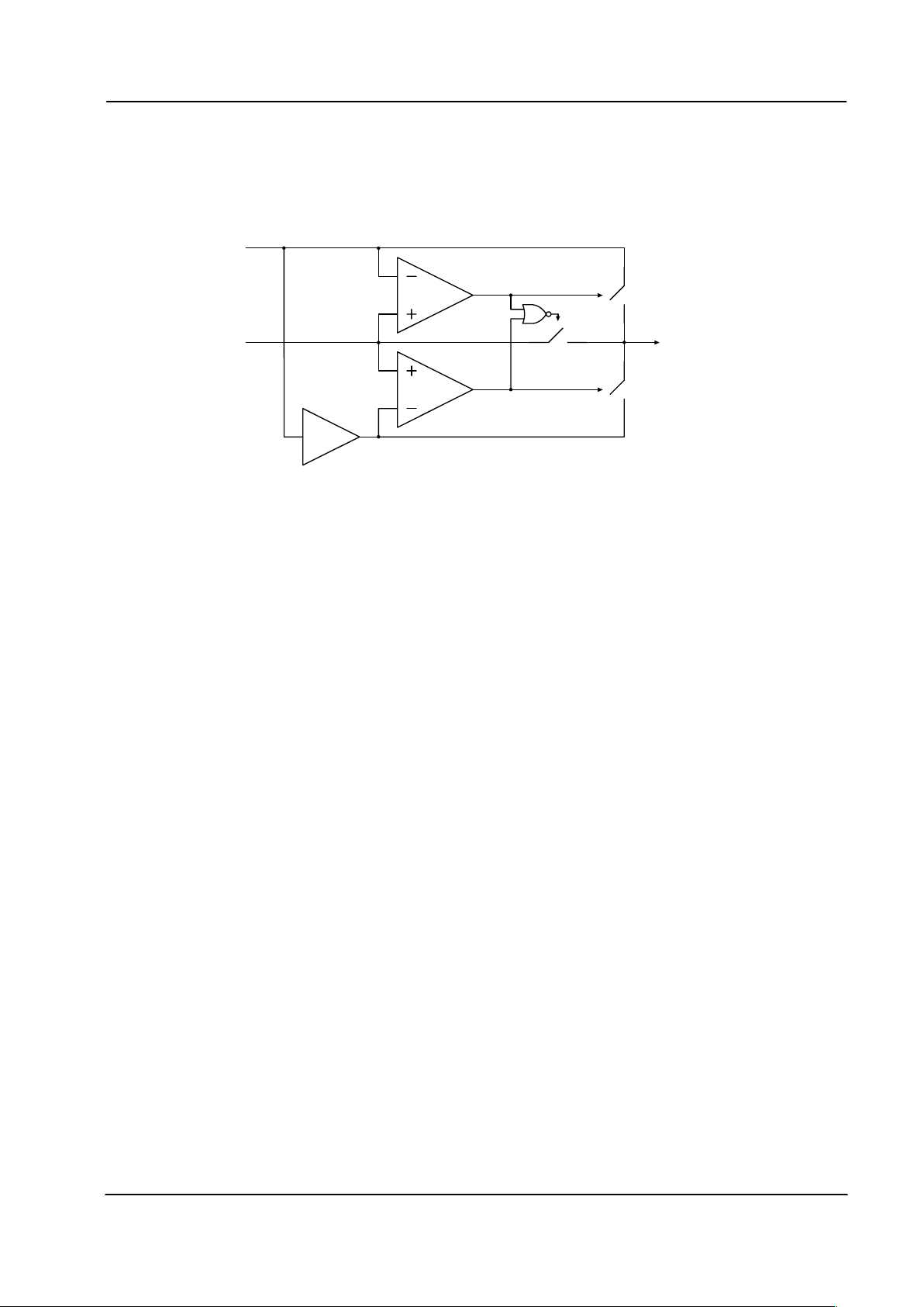
4.1.7 Audio Path without Deemphasis or Preemphasis
The magnitude response for the audio path (could apply to transmit or receive) without the preemphasis or
deemphasis is shown in Figure 13.
-70
-60
-50
-40
-30
-20
-10
0
10
100 1000 10000
Magnitude (dB)
Frequency (Hz)
NARROW BAND
WIDE BAND
Figure 13: Audio path frequency response without preemphasis or deemphasis.
FRS/PMR446/GMRS Family Radio Processor 17 CMX838 Advance Information
¤
¤¤
¤2001 MX-COM, Inc. www.mxcom.com Tel: 800 638 5577 336 744 5050 Fax: 336 744 5054 Doc. # 20480221.002
4800 Bethania Station Road, Winston-Salem, NC 27105-1201 USA All trademarks and service mark s are held by their res pec t ive companies.
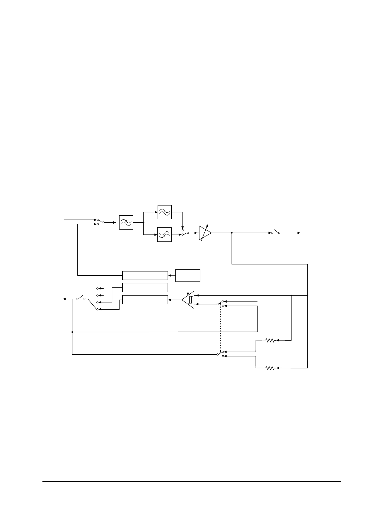
4.1.8 Deviation Limiter
The purpose of the deviation limiter is to limit the signal level at baseband prior to reaching the RF modulator.
This is necessary to avoid co-channel interference as well as conform to the spectral constraints stipulated by
regulatory agencies (e.g. FCC). Figure 14 is a block diagram of the limiter circuitry. Applying a DC voltage
between V
DD
and VDD/2 to the reference input sets the maximum peak-to-peak signal level. This reference is
internally set so the maximum signal level is 2.196V
P-P
and is constant over supply voltage.
-1
REF
I N
TX AUDIO
LIMITED SPEECH TO
POST DEVIATION
LIMITER FILTER
Figure 14: Deviation limiter block diagram.
FRS/PMR446/GMRS Family Radio Processor 18 CMX838 Advance Information
¤
¤¤
¤2001 MX-COM, Inc. www.mxcom.com Tel: 800 638 5577 336 744 5050 Fax: 336 744 5054 Doc. # 20480221.002
4800 Bethania Station Road, Winston-Salem, NC 27105-1201 USA All trademarks and service mark s are held by their res pec t ive companies.
4.2 Tone Signaling Processor
4.2.1 Tone encoding/decoding
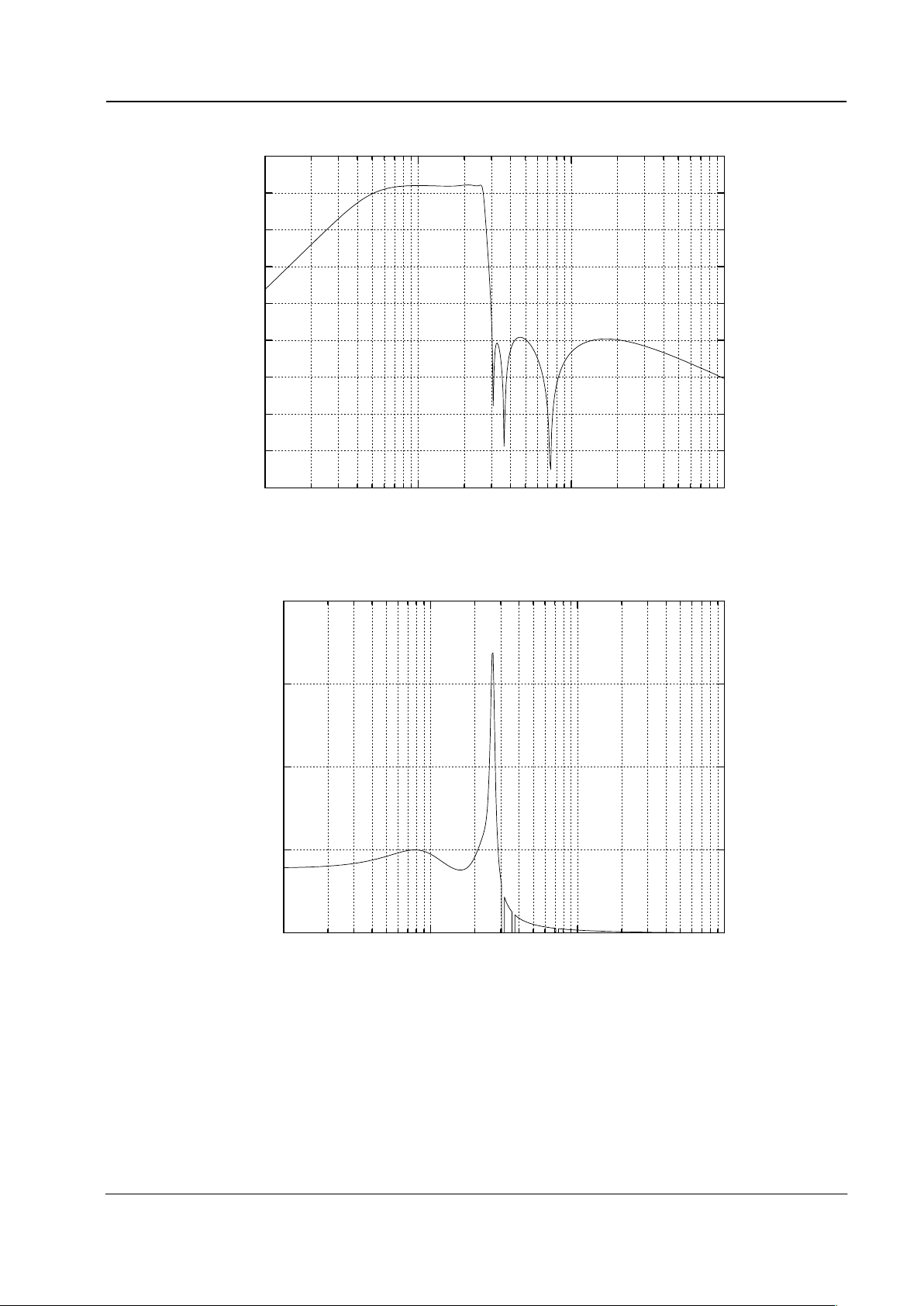
The tone signaling processor includes CTCSS encode and decode functions as well as an audio frequency
ringing/alert tone generator. The signaling processor is comprised of a configurable analog filter controlled by
the SUBAUDIO ANALOG CONTROL Register ($97) and a digital processor controlled by configuration tasks.
All device configuration data is passed over the device’s C-BUS serial interface. The configuration tasks to
setup the digital processor are simply C-BUS transaction sequences, which download task argument data
followed by a task request command. In typical applications, once the tone signaling processor is initialized,
its primary behavior (CTCSS encode and decode) is steered by the
RXTX/ bit of the SETUP Register ($80).
The subaudio filter is shared between transmit and receive. It is used to remove the speech signal from the
receive subaudio signal, leaving only the subaudible squelch signal as input to the digital processor. This filter
is also used to smooth the digitally generated subaudible signals in the transmit mode. Following the filter is a
gain trimmer stage that can adjust the signal level
±7.5dB in 0.5dB steps into the decoding section or out to
the modulation section. Approximately 20dB of gain is provided in the receive path and 20dB of attenuation in
the transmit path.
LPF1
CTCSS encode
CTCSS decoders
Band Gap
Reference
audio tone encode
V
BIAS
0
1
RXIN
to Modulation
Control Block
AUX
AUX Output
Control
Task
External DC
Restoration
Subaudio
Filter
Input
Select
Subaudio
HPF/LPF
Select
Subaudio
Filter
Output
Enable
Subaudio
LPF1
Gain
2 or 22db
HPF
LPF2
Subaudio
RX and TX
Levels
-7.5 to 7.5dB
External DC
Restoration
Control with
Initialization Tasks
Subaudio
LPF2
Gain
0 or -18dB
Figure 15: Subaudio Block Diagram
FRS/PMR446/GMRS Family Radio Processor 19 CMX838 Advance Information
¤
¤¤
¤2001 MX-COM, Inc. www.mxcom.com Tel: 800 638 5577 336 744 5050 Fax: 336 744 5054 Doc. # 20480221.002
4800 Bethania Station Road, Winston-Salem, NC 27105-1201 USA All trademarks and service mark s are held by their res pec t ive companies.
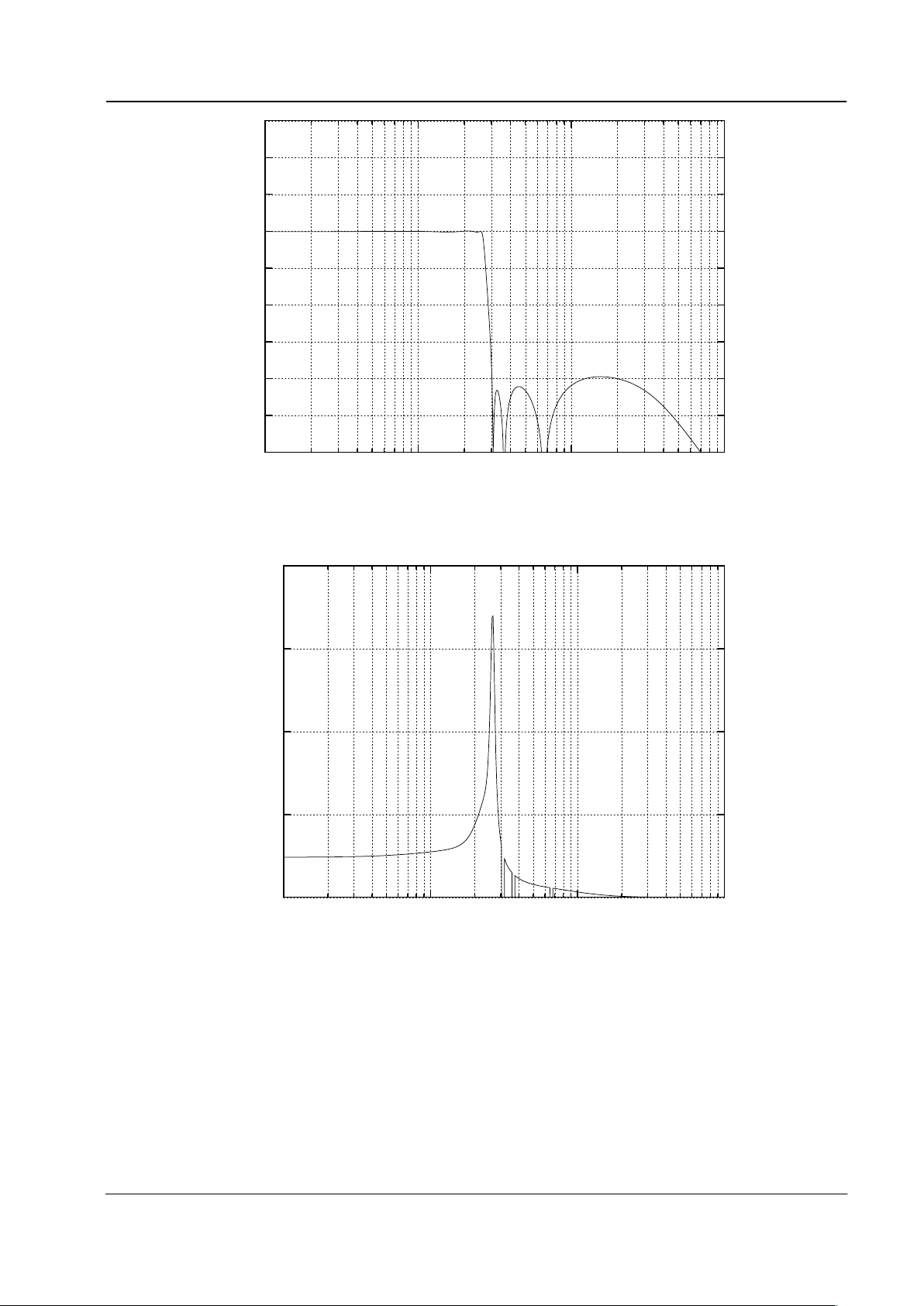
4.2.2 Subaudio RX and TX Filter Characteristics
-60
-50
-40
-30
-20
-10
0
10
20
30
10 100 1000 10000
Magnitude (dB)
Frequency (Hz)
Figure 16: Subaudio RX filter gain for normal CTCSS operation.
0
0.005
0.01
0.015
0.02
10 100 1000 10000
Delay (sec)
Frequency (Hz)
Figure 17: Subaudio RX filter delay for normal CTCSS operation.
FRS/PMR446/GMRS Family Radio Processor 20 CMX838 Advance Information
¤
¤¤
¤2001 MX-COM, Inc. www.mxcom.com Tel: 800 638 5577 336 744 5050 Fax: 336 744 5054 Doc. # 20480221.002
4800 Bethania Station Road, Winston-Salem, NC 27105-1201 USA All trademarks and service mark s are held by their res pec t ive companies.
-90
-80
-70
-60
-50
-40
-30
-20
-10
0
10 100 1000 10000
Magnitude (dB)
Frequency (Hz)
Figure 18: Subaudio TX level for normal CTCSS operation (Magnitude scale with respect to 0dBV)
0
0.005
0.01
0.015
0.02
10 100 1000 10000
Delay (sec)
Frequency (Hz)
Figure 19: Subaudio TX filter delay for normal CTCSS operation.
FRS/PMR446/GMRS Family Radio Processor 21 CMX838 Advance Information
¤
¤¤
¤2001 MX-COM, Inc. www.mxcom.com Tel: 800 638 5577 336 744 5050 Fax: 336 744 5054 Doc. # 20480221.002
4800 Bethania Station Road, Winston-Salem, NC 27105-1201 USA All trademarks and service mark s are held by their res pec t ive companies.
4.2.3 CTCSS Subaudio Decoder and Encoder Tone Set
The CMX838 supports all popular subaudio tones with a unique, full performance, 'one-of-any' rapid detect
capability that adds support for end product group calling and Tone Cloning™ features. The digital processor
essentially contains 51 decoders to analyze the receive signal. Each decoder can independently be enabled
or disabled via configuration tasks.
The result of the subaudio signal analysis is available in the subaudio status register ($94). Both a decode
status bit, and a decoder index number are reported in the status register. The decode status bit is a logic one
when an enabled decoder senses that the input signal matches its center frequency – the index number will
be that of the matching decoder. If the input signal does not contain a subaudio signal that matches an
enabled decoder’s center frequency then the status bit is a logic zero – in this case the decoder index number
is reported as:
A. 62 if there is a significant subaudio frequency present.
B. 63 if the no tone timer has expired indicating there is no significant subaudio frequency present now, or
C. 0 if no subaudio signal has been seen since the subaudio processor was enabled or most recently placed
in RX mode.
No. Frequency (Hz) No. Frequency (Hz)
1. 67.0 27. 159.8*
2. 69.3 28. 162.2
3. 71.9 29. 165.5*
4. 74.4 30. 167.9
5. 77.0 31. 171.3*
6. 79.7 32. 173.8
7. 82.5 33. 177.3*
8. 85.4 34. 179.9
9. 88.5 35. 183.5*
10. 91.5 36. 186.2
11. 94.8 37. 189.9*
12. 97.4 38. 192.8
13. 100.0 39. 196.6*
14. 103.5 40. 199.5*
15. 107.2 41. 203.5
16. 110.9 42. 206.5*
17. 114.8 43. 210.7
18. 118.8 44. 218.1
19. 123.0 45. 225.7
20. 127.3 46. 229.1*
21. 131.8 47. 233.6
22. 136.5 48. 241.8
23. 141.3 49. 250.3
24. 146.2 50. 254.1*
25. 151.4 51. User Programmable
26. 156.7
* Subaudible Tones not included in TIA-603 standard
Table 2: CTCSS Subaudio Tone Frequencies with their Corresponding Index Number
 Loading...