MX COM Inc CMX808AE2 Datasheet

DATA BULLETIN
CMX808A
1999 MX-COM, Inc. www.mxcom.com tel: 800 638 5577 336 744 5050 fax: 336 744 5054 Doc. # 20480199.002
4800 Bethania Station Road, Winston-Salem, NC 27105-1201 USA All trademarks and service marks are held by their respective companies.
Family Radio Service
CTCSS Processor
PRELIMINARY INFORMATION
Features
•
Rapid multi-tone CTCSS decoder
supports new end user features
•
Fast Tone Decode (150ms)
•
Supports Tones from 62.5Hz to 251Hz
•
Integrated 32 Step Digital Volume
Control (-48.0dB to 0dB + Off)
•
Tone Cloning Capabilities
•
Sub-Audio Tone Rejection Filter
•
Low Power 3.0V to 5.5V Operation
•
Very small 20-pin TSSOP Package
•
4.0MHz Xtal/Clock Oscillator
Applications
•
Family Radio Service (FRS) Radios
•
Amateur Radio Equipment
•
General Mobile Radio Service (GMRS)
•
Short Range Business Radio
MODULATOR
DISCRIMINATOR
HOST
µC
KEYPAD
DISPLA Y
RADIO
CMX808A
RF
Tx
SERIAL 'C-BUS'
DATA & CONTR OL
Rx
FAST CTCSS
AUDIO FILTER
VOLUME CONTROL
The CMX808A is a programmable CTCSS encoder/decoder optimized for Family Radio Service transceivers
through a combination of leading edge performance, low cost, small size, and low power. With rapid
response time and the ability to decode one-of-many possible tones, the decoder enables practical tone
scanning to allow an FRS radio to quickly decode received CTCSS tones by 'listening' to the CTCSS tone
transmissions of other FRS radios. This feature can be used to:
1. Readily support both individual (one person) and group (e.g. children vs. adults) call codes.
2. Support quick and automatic resolution of radio user frustration caused by mismatched CTCSS tone
configurations in CTCSS-based FRS radios. In some cases, this approach can be used to match
CTCSS tone decoder configurations to different vendors' CTCSS-based FRS radios when supported
tone sets are not clearly documented or well understood.
With integrated digital volume control and a simple serial control interface, the CMX808A features very low
power consumption and small size. The CMX808A requires a 3.0V to 5.5V power supply and is available in
the following packages: 20-pin TSSOP (CMX808AE3) and 24-pin PDIP (CMX808AP4).

Family Radio Service CTCSS Processor 2 CMX808A Preliminary Information
1999 MX-COM, Inc. www.mxcom.com tel: 800 638 5577 336 744 5050 fax: 336 744 5054 Doc. # 20480199.002
4800 Bethania Station Road, Winston-Salem, NC 27105-1201 USA All trademarks and service marks are held by their respective companies.
CONTENTS
Section Page
1 Block Diagram................................................................................................................3
2 Signal List.......................................................................................................................4
3 External Components....................................................................................................6
4 General Description.......................................................................................................7
4.1 Software Description ........................................................................................................... 7
4.1.1 Address/Commands...............................................................................................................7
4.1.2 Write Only Register Description .............................................................................................7
4.1.3 Read Only Register Description...........................................................................................12
5 Application Notes ........................................................................................................15
5.1 General.............................................................................................................................. 15
5.2 Transmitter ........................................................................................................................ 15
5.3 Tx Tone Table ................................................................................................................... 16
5.4 Receiver (Decode)............................................................................................................. 16
5.5 Rx Tone Table................................................................................................................... 17
6 Performance Specification..........................................................................................18
6.1 Electrical Performance ...................................................................................................... 18
6.1.1 Absolute Maximum Ratings.................................................................................................. 18
6.1.2 Operating Limits...................................................................................................................18
6.1.3 Operating Characteristics.....................................................................................................19
6.1.4 Timing Diagrams..................................................................................................................21
6.2 Packaging.......................................................................................................................... 22
MX-COM, Inc. reserves the right to change specification at any time and without notice.

Family Radio Service CTCSS Processor 3 CMX808A Preliminary Information
1999 MX-COM, Inc. www.mxcom.com tel: 800 638 5577 336 744 5050 fax: 336 744 5054 Doc. # 20480199.002
4800 Bethania Station Road, Winston-Salem, NC 27105-1201 USA All trademarks and service marks are held by their respective companies.
1 Block Diagram
CLOCK OSCILLATOR
AND DIVIDERS
SUB AUDIO
LPF
AUDIO
FILTER
CTCSS Tx TONE
GENERATOR
'C-BUS'
INTERFACE
AND
CONTROL
LOGIC
A to D
CONVERTER
CTCSS TONE
DECODER
V
BIASVSS
V
DD
C6
C4
TX AUDIO IN
TX AUDIO
INPUT
R1
-
+
CTCSSTx
AUDIOTx / Rx
RX AMP
Enable
V
BIAS
RXAMPOUT
RXAMPIN
C3
XT AL
XT AL/CLOCK
C5
R3
R4
C7
Input from
Demodulator
C1
C2
X1
C8
A/D CAP CTCSS Rx
TX SUB AUDIO OUT TX AUDIO OUT RX AUDIO OUT
VOLUME OUT
COMMAND DATA
REPLY DATA
CS
IRQ
SERIAL CLOCK
V
DD
R2
Enable
Volume
Control
VOLUME IN
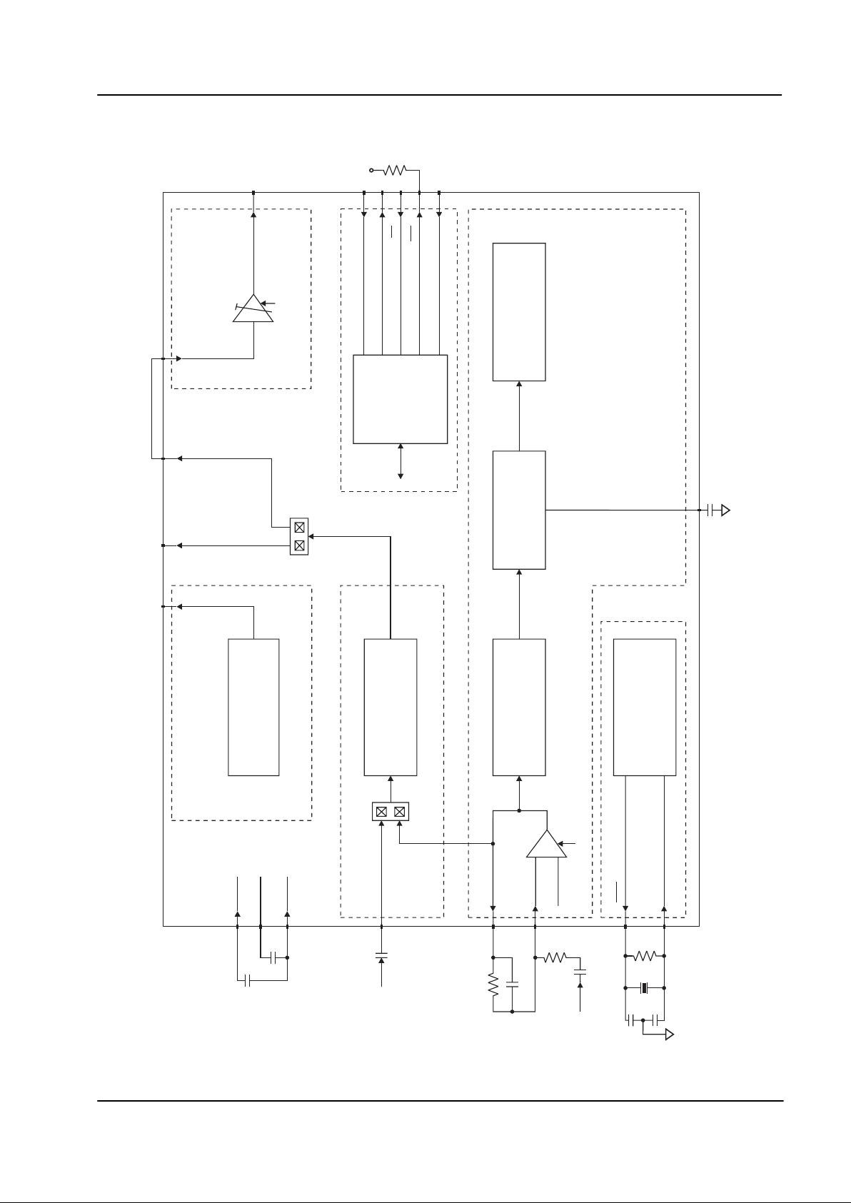
Figure 1: Block Diagram

Family Radio Service CTCSS Processor 4 CMX808A Preliminary Information
1999 MX-COM, Inc. www.mxcom.com tel: 800 638 5577 336 744 5050 fax: 336 744 5054 Doc. # 20480199.002
4800 Bethania Station Road, Winston-Salem, NC 27105-1201 USA All trademarks and service marks are held by their respective companies.
2 Signal List
Package /
Pin No
Signal
E3 P4 Name Type
Description
11
XTAL
output The inverted output of the on-chip oscillator.
2 2 XTAL/CLOCK input
The input to the on-chip oscillator, for external Xtal circuit or
clock.
3 3 SERIAL CLOCK input
The "C-BUS" serial clock input. This clock, produced by the
µC, is used for transfer timing of commands and data to and
from the device. See Figure 6.
4 4 COMMAND DATA input
The "C-BUS" serial data input from the µC. Data is loaded
into this device in 8-bit bytes, MSB (D7) first, and LSB (D0)
last, synchronized to the SERIAL CLOCK. See Figure 6.
5 5 REPLY DATA output
The "C-BUS" serial data output to the µC. The transmission
of REPLY DATA bytes is synchronized to the SERIAL
CLOCK under the control of the
CS
input. This 3-state
output is held at high impedance when not sending data to
the µC. See Figure 6.
66
CS
input
The "C-BUS" data loading control function: this input is
provided by the µC. Data transfer sequences are initiated,
completed or aborted by the
CS signal. See Figure 6.
77
IRQ
output
This output indicates an interrupt condition to the µC by
going to a logic "0". This is a "wire-ORable" output,
enabling the connection of up to 8 peripherals to 1 interrupt
port on the µC. This pin has a low impedance pulldown to
logic "0" when active and a high-impedance when inactive.
An external pull-up resistor is required. An interrupt is
effective if not masked out by the IRQ MASK (bit 0 in the
SUB-AUDIO CONTROL register $80).
88 NC
9NC
No internal connection. Do not make any connection to
these pins.
9 10 A/D CAP output
An internal reference voltage for the A to D converter,
decoupled to V
SS
by an external capacitor.
11 NC
No internal connection. Do not make any connection to this
pin.
10 12 V
SS
Power The negative supply rail (ground).
11 13 V
BIAS
output
A bias line for the internal circuitry, held at V
DD
/2. This pin
must be decoupled by a capacitor mounted close to the
device pins.
12 14 RX AMP IN input The inverting input to the Rx input amplifier.
13 15 RX AMP OUT output
The output of the Rx input amplifier and the input to the
audio filter section.
14 16 RX AUDIO OUT output Output of the Rx audio filter section.
17 NC
No internal connection. Do not make any connection to this
pin.
15 18 TX AUDIO IN input Input to the Tx audio filter section.
16 19 TX AUDIO OUT output Output of the Tx audio filter section.
17 20 VOLUME IN input Input to the audio volume control.
18 21 TX SUB AUDIO OUT output Output of the CTCSS tone generator.
19 22 VOLUME OUT output Output of the audio volume control.

Family Radio Service CTCSS Processor 5 CMX808A Preliminary Information
1999 MX-COM, Inc. www.mxcom.com tel: 800 638 5577 336 744 5050 fax: 336 744 5054 Doc. # 20480199.002
4800 Bethania Station Road, Winston-Salem, NC 27105-1201 USA All trademarks and service marks are held by their respective companies.
Package /
Pin No
Signal
E3 P4 Name Type
Description
23 NC
No internal connection. Do not make any connection to this
pin.
20 24 V
DD
Power
The positive supply rail. Levels and voltages are dependent
upon this supply. This pin should be decoupled to V
SS
by a
capacitor.
Table 1: Signal List

Family Radio Service CTCSS Processor 6 CMX808A Preliminary Information
1999 MX-COM, Inc. www.mxcom.com tel: 800 638 5577 336 744 5050 fax: 336 744 5054 Doc. # 20480199.002
4800 Bethania Station Road, Winston-Salem, NC 27105-1201 USA All trademarks and service marks are held by their respective companies.
3 External Components
V
DD
V
DD
V
SS
V
DD
V
BIAS
IRQ
XTAL
A/D CAP
SERIAL CLOCK
"C-BUS"
INTERFAC E
COMMAND DA TA
XTAL/CLOCK
RX AMP IN
R3
R4
R2
Input from
Demodulator
Tx Audio Input
CMX808AE3
TX SUB AUDIO OUT
C4
C8
C5
C3
C7
C6
REPLY DATA
CS
NC
RX AMP OUT
RX AUDIO OUT
VOLUME OUT
VOLUME IN
TX AUDIO IN
TX AUDIO OUT
1
2
3
4
5
6
8
9
10
11
12
13
14
7
20
19
18
17
16
15
XTAL
XTAL/CLOCK
C1
C2
X1
R1
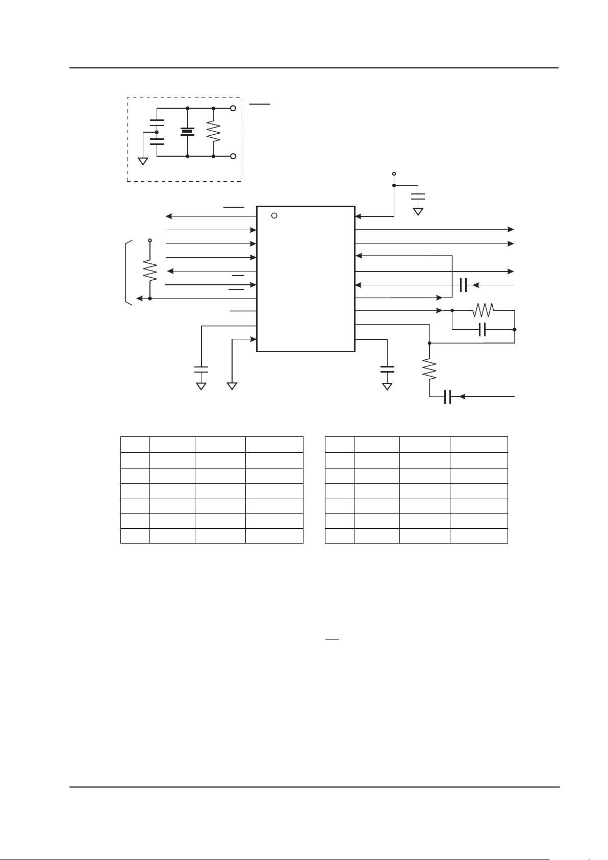
Figure 2: Recommended External Components
R1 1M
: ±5% C4 0.1µF ±20%
R2 22k: ±10% C5 100pF ±20%
R3 100k: ±10% C6 0.1µF ±20%
R4 Note 1 ±10% C7 Note 1 ±20%
C1 22pF ±20% C8 0.1µF ±20%
C2 22pF ±20%
C3 0.1µF ±20% X1 Note 2 4.0MHz ±100ppm
Table 2: Recommended External Components
Recommended External Component Notes:
1. R3, R4, C5 and C7 form the gain components for the Rx Input Amplifier. R4 should be chosen as required
by the signal level, using the following formula:
R4
R3
- Gain =
C7 x R4 should be chosen so as not to compromise the low frequency performance of this product.
2. For best results, a crystal oscillator design should drive the clock inverter input with signal levels of at
least 40% of V
DD
, peak to peak. Tuning fork crystals generally cannot meet this requirement. To obtain
crystal oscillator design assistance, please consult your crystal manufacturer.

Family Radio Service CTCSS Processor 7 CMX808A Preliminary Information
1999 MX-COM, Inc. www.mxcom.com tel: 800 638 5577 336 744 5050 fax: 336 744 5054 Doc. # 20480199.002
4800 Bethania Station Road, Winston-Salem, NC 27105-1201 USA All trademarks and service marks are held by their respective companies.
4 General Description
The CMX808A is a programmable CTCSS Processor for Family Radio Service, see Figure 1.
The receiver of the CMX808A decodes a user-programmable set of up to 7 tones with minimum software
intervention; the band-pass filter is designed to filter out the CTCSS sub-audio tones. A high-resolution tone
encoder performs accurate generation of CTCSS tones.
Each function, and the routing of signals, is flexible and may be configured or controlled by the user's
software.
4.1 Software Description
4.1.1 Address/Commands
Instructions and data are transferred, via "C-BUS", in accordance with the timing information given in Figure
6.
Instruction and data transactions to and from the CMX808A consist of an Address/Command (A/C) byte,
which may be followed by either:
(i) a further instruction or data (1 or 2 bytes) or
(ii) a status or Rx data reply (1 byte)
4.1.2 Write Only Register Description
HEX
ADDRESS/
COMMAND
REGISTER
NAME
BIT 7
(D7)
BIT 6
(D6)
BIT 5
(D5)
BIT 4
(D4)
BIT 3
(D3)
BIT 2
(D2)
BIT 1
(D1)
BIT 0
(D0)
$01
GENERAL
RESET
N/A N/A N/A N/A N/A N/A N/A N/A
CTCSS CTCSS DECODER BANDWIDTH
$80
SUB-AUDIO
CONTROL
TX
ENABLE
DECODER
ENABLE
MSB
BIT 3 BIT 2 BIT 1
LSB
BIT 0
0
CTCSS
IRQ
MASK
AUDIO ATTENUATION
$82
AUDIO
CONTROL
TX BPF
ENABLE
RX BPF
ENABLE
BPF
UN-
MUTE
MSB
BIT 4
BIT 3 BIT 2 BIT 1
LSB
BIT 0
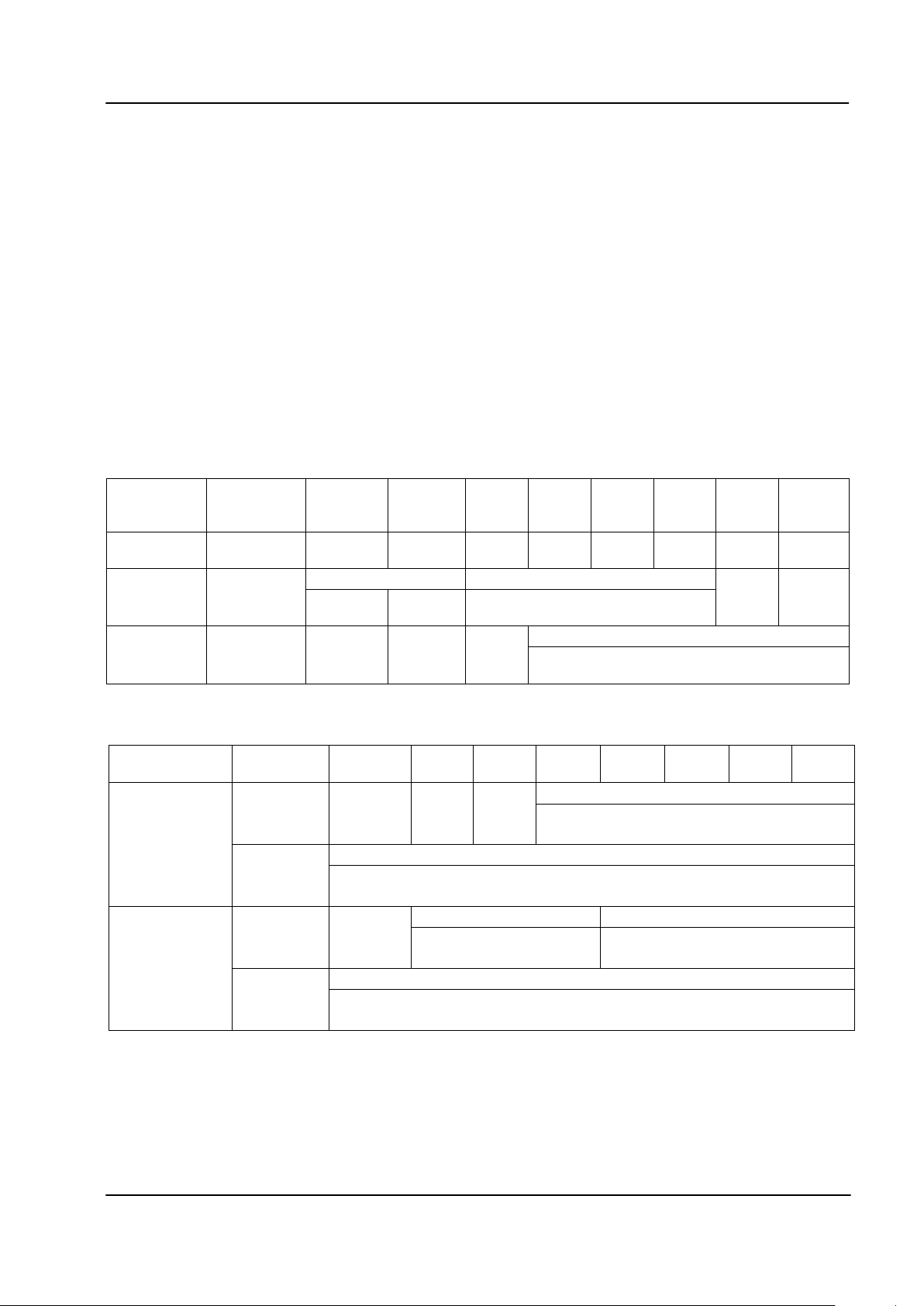
Table 3: 8-bit Write Only Registers
HEX ADDRESS/
COMMAND
REGISTER
NAME
BIT 7
(D7)
BIT 6
(D6)
BIT 5
(D5)
BIT 4
(D4)
BIT 3
(D3)
BIT 2
(D2)
BIT 1
(D1)
BIT 0
(D0)
CTCSS TX FREQUENCY
CTCSS
TX FREQ.
(Byte 1)
CTCSS
TX
NOTONE
00
MSB
BIT 12 BIT 11 BIT 10 BIT 9 BIT 8
CTCSS TX FREQUENCY
$83
CTCSS
TX FREQ.
(Byte 2)
BIT 7 BIT 6 BIT 5 BIT 4 BIT 3 BIT 2 BIT 1
LSB
BIT 0
CTCSS TONE ADDRESS CTCSS FREQUENCY
CTCSS RX
PROGRAM
(Byte 1)
0
MSB
BIT2
BIT 1
LSB
BIT 0
MSB
BIT 11 BIT 10 BIT 9 BIT 8
CTCSS FREQUENCY
$84
CTCSS RX
PROGRAM
(Byte 2)
BIT 7 BIT6 BIT 5 BIT 4 BIT 3 BIT 2 BIT 1
LSB
BIT 0
Table 4: 16-bit Write Only Registers
4.1.2.1 GENERAL RESET (Hex address $01)
The reset command has no data attached to it. It sets the device registers to zero (all powersaved) with the
exception of Bits 2, 1 and 0 of the SUB-AUDIO STATUS register $81.
 Loading...