MX COM Inc CMX673P1, CMX673E3, CMX673D4 Datasheet

COMMUNICATION ICs
DATA BULLETIN
CMX673
Call Progress Tone
Detector
2000 MX-COM, Inc www.mxcom.co m Tel: 800 638 5577 336 744 5050 Fax: 336 744 5054 Doc. # 20480182.006
4800 Bethania Station Road, Winston-Salem, NC 27105-1201 USA All Trademarks and service marks are held by their respective companies.
PRELIMINARY INFORMATION
Features Applications
•
Worldwide Tone Compatibility
•
Fast Response
Stutter Dial Tone
Single and Dual Tones
•
Industry Compatible Pin Out
•
Wide Dynamic Signal Range
•
Low Power: 0.5mA at 3.0V
•
3.0V to 5.0V Operation
•
3.58MHz Xtal/Clock Oscillator
•
Worldwide Payphone Systems
•
Featurephone active feature confirmation
•
Telephone Redialing Systems
•
Dialing Modems
•
Banking and Billing Systems
•
Telecom Test Equipment
•
Telecom Security Systems
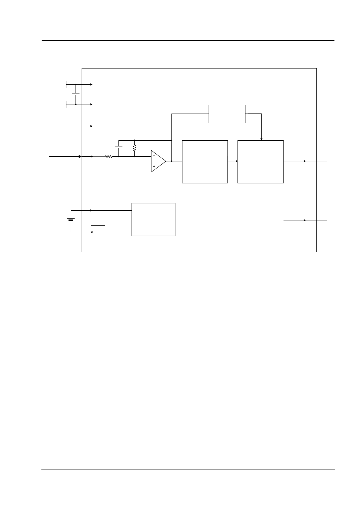
LEVEL
DETECTOR
AMPLIFIER
ENABLE
CALL
PROGRESS
DETECT
SIGNAL
ANALYZER
CONTROL
AND
OUTPUT
LOGIC
CALL PROGRESS
DETECTOR
SIGNAL
INPUT
The CMX673 is a low voltage multi-purpose Call Progress Tone detector for use in Public Switched
Telephone Network System (PSTN) applications. Call progress detection allows equipment that dials into the
PSTN to monitor the progress of the resulting call. Various states such as Ringing, Busy, Not available, and
Answer can be determined. Using digital signal processing techniques the CMX673 accurately analyzes
tones in the 315Hz to 650Hz frequency band and distinguishes valid call progress tone signals from line noise
or voice. This contrasts with other call progress detection devices that are based on simple filtering
techniques. When combined with cadence measurement of the CMX673 output, the rapid detect response
time of the CMX673 allows it to support a wide range of call progress functions including ‘stutter dial tone’
detection used in voice messaging systems.
A single, low cost 3.58MHz crystal ensures accurate and repeatable performance. With supply requirements
between 2.7V and 5.5V the CMX673 is easily integrated into a wide range of telecom applications.
The convenient CMX673 pin out allows it to be readily incorporated into existing product designs to quickly
achieve its benefits. Small geometry CMOS design techniques provide a complete call progress detector that
analyzes both frequency and amplitude in a small single package. Available packages are: 8-pin PDIP
(CMX673P1), 16-pin SOIC (CMX673D4), and 20-pin TSSOP (CMX673E3).

Call Progress Tone Detector 2 CMX673 Preliminary Information
2000 MX-COM, Inc www.mxcom.com Tel: 800 638 5577 336 744 5050 Fax: 336 744 5054 Doc. # 20480182.006
4800 Bethania Station Road, Winston-Salem, NC 27105-1201 USA All Trademarks and service marks are held by their respective companies.
CONTENTS
Section Page
1 Block Diagram................................................................................................................3
2 Signal List.......................................................................................................................4
3 External Components....................................................................................................5
4 General Description.......................................................................................................5
4.1 Overall Function Description ............................................................................................... 5
4.2 Glossary .............................................................................................................................. 6
4.3 Block Diagram Description.................................................................................................. 6
4.4 Decode Output Truth Table................................................................................................. 6
5 Application Notes ..........................................................................................................7
5.1 General................................................................................................................................ 7
5.1.1 Typical Telephone Line Circuit...............................................................................................7
6 Performance Specification............................................................................................8
6.1 Electrical Performance ........................................................................................................ 8
6.1.1 Absolute Maximum Ratings....................................................................................................8
6.1.2 Operating Limits.....................................................................................................................8
6.1.3 Operating Characteristics.......................................................................................................9
6.1.4 Timing...................................................................................................................................10
6.2 Packaging.......................................................................................................................... 10
MX-COM, Inc. reserves the right to change specifications at any time and without notice.

Call Progress Tone Detector 3 CMX673 Preliminary Information
2000 MX-COM, Inc www.mxcom.com Tel: 800 638 5577 336 744 5050 Fax: 336 744 5054 Doc. # 20480182.006
4800 Bethania Station Road, Winston-Salem, NC 27105-1201 USA All Trademarks and service marks are held by their respective companies.
1 Block Diagram
V
REF
V
REF
LEVEL
DETECTOR
XTAL/CLOCK
XTAL
C2
X1
CLOCK
OSCILLATO R
AND
DIVIDERS
AMPLIFIER
SIGIN
ENABLE
DETECT
SIGNAL
ANALYZER
CONTROL
AND
OUTPUT
LOGIC
CALL PROGRESS
DETECTOR
SIGNAL
INPUT
V
DD
V
DD
V
SS
V
SS
Figure 1: Block Diagram

Call Progress Tone Detector 4 CMX673 Preliminary Information
2000 MX-COM, Inc www.mxcom.com Tel: 800 638 5577 336 744 5050 Fax: 336 744 5054 Doc. # 20480182.006
4800 Bethania Station Road, Winston-Salem, NC 27105-1201 USA All Trademarks and service marks are held by their respective companies.
2 Signal List
Packages Signal Description
E3 D4 P1 Name Type
3 2 1 XTAL/CLOCK input The input to the on-chip oscillator and external clock
input. Components are on chip.
5 4 2
XTAL
output The inverted output of the on-chip oscillator.
7 5 3 ENABLE input A logic ‘1’ applied to this input enables the DETECT
output. A logic ‘0’ will reset DETECT output to a logic
‘0’.
8 7 4 DETECT output When a call progress signal is detected, this output
goes to a logic ‘1’.
13 10 5 SIGIN input Signal input. Signals to this pin should be AC coupled.
The DC bias of this pin is set internally.
15 12 6 VSS Power The negative supply rail (ground).
17 14 7 V
REF
output Internally generated reference voltage, held at VDD/2
18 15 8 VDD Power The positive supply rail. This pin should be bypassed
to V
SS
by a capacitor.
1, 2
4, 6
9, 10
11, 12
14, 16
19, 20
1, 3
6, 8
9, 11
13, 16
NC Internal Connection. Do not make any connection to
these pins.
Table 1: Signal List
 Loading...