MX COM Inc CMX654P3, CMX654D4 Datasheet

DATA BULLETIN
CMX654
¤1998 MX-COM, Inc. www.mxcom.com Tel: 800 638 5577 336 744 5050 Fax: 336 744 5054 Doc. # 20480186.001
4800 Bethania Station Road, Winston-Salem, NC 27105-1201 USA All Trademarks and Service marks are held by their respective companies.
V.23 TRANSMIT
MODULATOR
PRELIMINARY INFORMATION
Features Applications
x 1200bits/sec, V.23 Transmit Modulator
x 3.0V to 5.5V Supply:
1mA typical at 3V
x Zero Power Mode:
1µA typical
x 1200bits/sec Tx Data Retiming
x 3.58MHz Xtal/Clock Rate
x Meets ITU and ETSI Specifications
x Caller ID generation for:
ISDN Terminal Adapters
Wireless Local Loop System
ISDN PABX Applications
Pair-Gain Systems
Public Switched Telephone
Networks
Trunk Exchanges
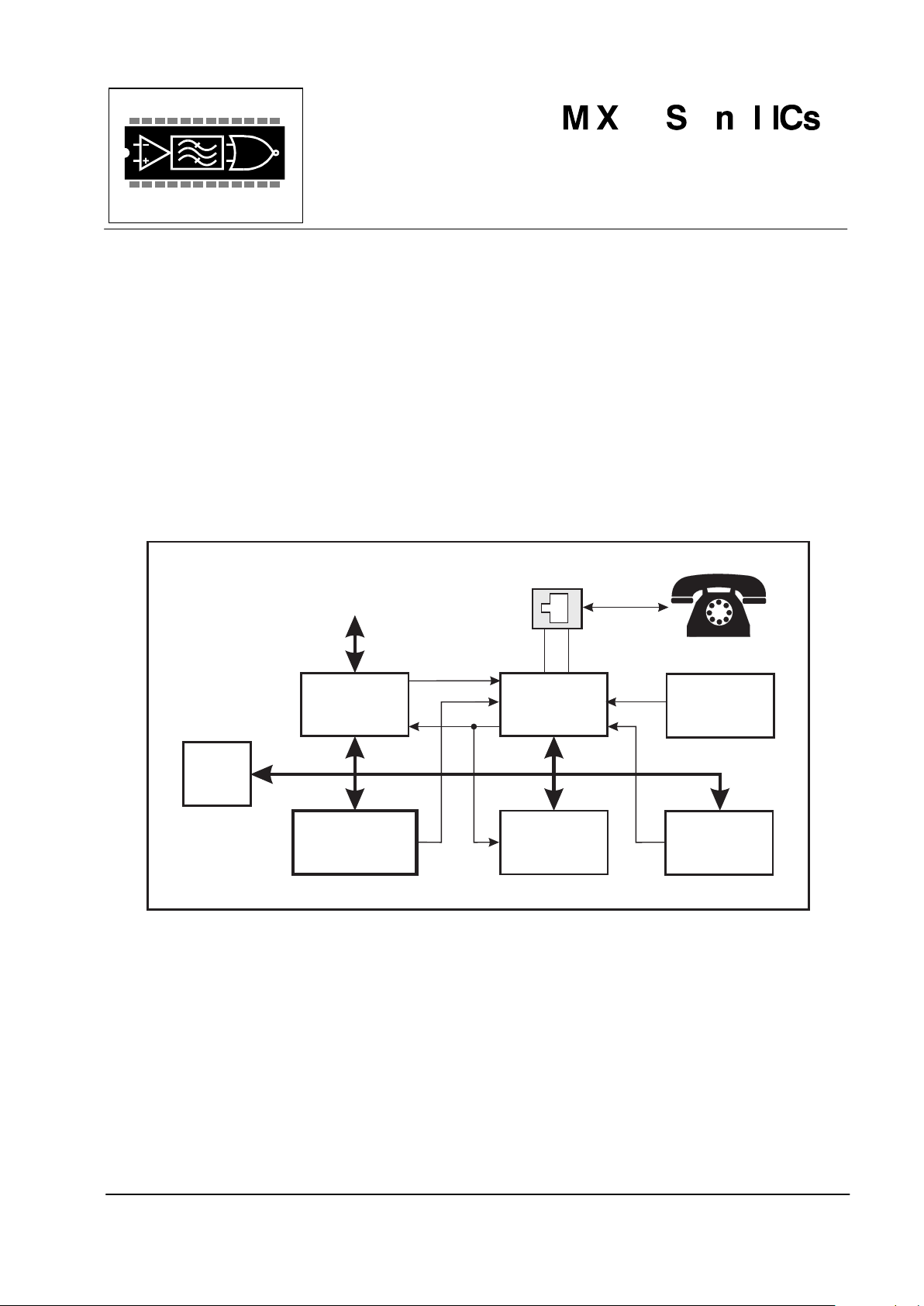
Digital
Line Circuit
CODEC
µC
V23T ransmit
Modulator
SLIC
DTMF
DECODER
RINGING
GENERATOR
DC-to-DC
CONVERTER
POTS
CMX654
The CMX654 is a low power integrated circuit, designed for the transmission of asynchronous 1200bits/sec
data in accordance with ITU, V.23 and ETSI specifications.
The device incorporates an optional Tx data retiming function. This device may be operated so that only the
mark or space tone is produced.
The CMX654 may be used in a wide range of telephone telemetry systems. With a low voltage requirement of
3.0V it is suitable for both portable terminal and line powered applications. A very low current 'sleep' mode
(1PA typ.) and an operating current of 1mA typ. makes the CMX654 ideal for line powered applications.
This device requires a standard 3.58MHz Xtal/Clock rate and operates from a 3.0 to 5.5V supply. Available
packages are: 16-pin SOIC (CMX654D4) and 16-pin PDIP (CMX654P3). Additional package styles may be
available to meet specific design requirements.

V.23 Transmit Modulator 2 CMX654 PRELIMINARY INFORMATION
¤1998 MX-COM, Inc. www.mxcom.com Tel: 800 638 5577 336 744 5050 Fax: 336 744 5054 Doc. # 20480186.001
4800 Bethania Station Road, Winston-Salem, NC 27105-1201 USA All Trademarks and Service marks are held by their respective companies.
CONTENTS
Section Page
1 Block Diagram................................................................................................................3
2 Signal List.......................................................................................................................4
3 External Components....................................................................................................5
4 General Description.......................................................................................................6
4.1 Xtal Oscillator and Clock Dividers ....................................................................................... 6
4.2 Mode Control Logic ............................................................................................................. 6
4.3 FSK Modulator and Transmit Filter...................................................................................... 6
4.4 Tx Data Retiming................................................................................................................. 7
5 Application Notes ..........................................................................................................8
5.1 Line Interface....................................................................................................................... 8
6 Performance Specification............................................................................................9
6.1 Electrical Performance ........................................................................................................ 9
6.1.1 Absolute Maximum Ratings....................................................................................................9
6.1.2 Operating Limits.....................................................................................................................9
6.1.3 Operating Characteristics.....................................................................................................10
6.2 Timing................................................................................................................................ 11
6.3 Packaging.......................................................................................................................... 12
MX-COM, Inc reserves the right to change specification at any time and without notice.

V.23 Transmit Modulator 3 CMX654 PRELIMINARY INFORMATION
¤1998 MX-COM, Inc. www.mxcom.com Tel: 800 638 5577 336 744 5050 Fax: 336 744 5054 Doc. # 20480186.001
4800 Bethania Station Road, Winston-Salem, NC 27105-1201 USA All Trademarks and Service marks are held by their respective companies.
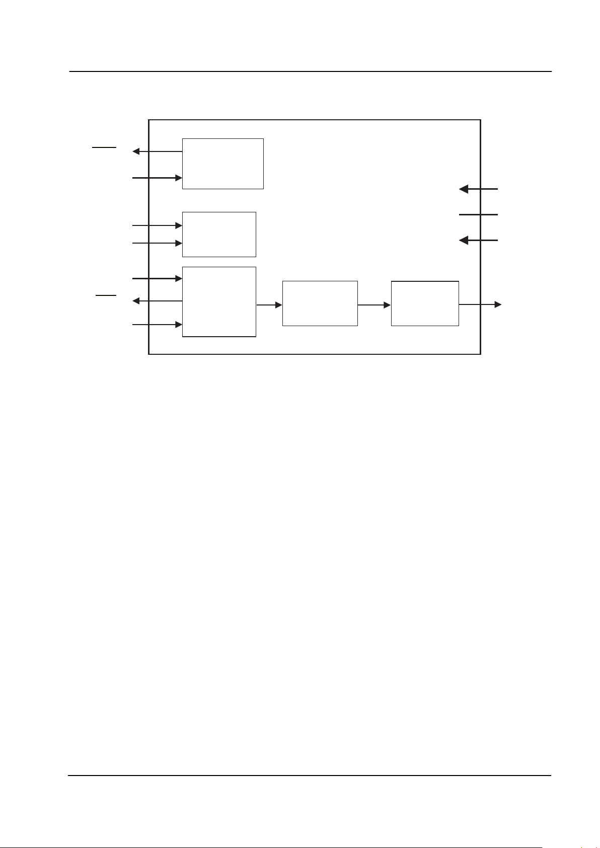
1 Block Diagram
TXD
M0
CLK
RDY
M1
Mode
Control
Logic
Tx Data
Re-timing
Transmit
Filter and
Output Buffer
FSK
Modulator
TXOUT
Xtal Osc and
Clock Dividers
XTAL/
CLOCK
XTAL
V
DD
V
BIAS
V
S
S
CMX654
Figure 1: Block Diagram

V.23 Transmit Modulator 4 CMX654 PRELIMINARY INFORMATION
¤1998 MX-COM, Inc. www.mxcom.com Tel: 800 638 5577 336 744 5050 Fax: 336 744 5054 Doc. # 20480186.001
4800 Bethania Station Road, Winston-Salem, NC 27105-1201 USA All Trademarks and Service marks are held by their respective companies.
2 Signal List
D4/P3 Signal Description
Pin No. Name Type
1
XTAL
input The output of the on-chip Xtal oscillator inverter.
2 XTAL/CLOCK input The input to the on-chip Xtal oscillator inverter.
3 M0 input A logic level input for setting the mode of the device.
See Section 4.2.
4 M1 input A logic level input for setting the mode of the device.
See Section 4.2.
5 Connect to VSS.
6 N/C No connection, do not connect to this pin.
7 TXOUT output The output of the FSK generator.
8V
SS
Power The negative supply rail (ground).
9V
BIAS
output Internally generated bias voltage, held at VDD/2 when the device is
not in 'Zero-Power' mode. Should be decoupled to V
SS
by a
capacitor mounted close to the device pins.
10 - - Connect to V
DD
.
11 TXD input A logic level input for either the raw input to the FSK Modulator or
data to be re-timed depending on the state of the M0, M1 and CLK
inputs. See Section 4.3.
12 CLK input A logic level input which may be used to clock data bits into the Tx
FSK Data Retiming block.
13 - N/C No connection, do not connect to this pin.
14 - N/C No connection, do not connect to this pin.
15
RDY
output "Ready for Tx data transfer" output of the on-chip data retiming
circuit. This open-drain active low output may be used as an
Interrupt Request/Wake-up input to the associated PC. An external
pull-up resistor should be connected between this output and V
DD
.
16 V
DD
Power The positive supply rail. Levels and thresholds within the device
are proportional to this voltage. Should be decoupled to V
SS
by a
capacitor mounted close to the device pins.
VDD and V
BIAS
decoupling is very important. It is recommended that the decoupling capacitors be placed
so that connections between them and the device pins are as short as practicable.
Table 1: Signal List
 Loading...