DATA BULLETIN
CMX644A
2000 MX-COM, Inc. www.mxcom.com tel: 800 638 5577 336 744 5050 fax: 336 744 5054 Doc. # 20480197.006
4800 Bethania Station Road,Winston-Salem,NC 27105-1201 USA All trademarks and service marks are held by their respective companies.
Bell 212A and V.22 Modem
with Call Progress and DTMF
PRELIMINARY INFORMATION
Features
• Bell 212A and V.22 Compatible Modem
• 1200bps Full Duplex Operation (2 or 4 Wire)
• UART for Start/Parity/Stop bit processing
• Non-UART Operating Mode
• Software Adjustable Tx and Rx Levels
• Programmable Group Delay Equalizer
• Answer/Originate Tone Generator/Detector
• Call Progress Tone Detection
• Integrated DTMF Encoder
• Line Reversal and Ring Detector
• Hook Switch Relay Driver
• Flexible Xtal/Master Clock Selection
• Simple Serial Control Interface
• Zero-Power Standby Mode
• 3.0V to 5.0V Operation
Applications
• Telephone Telemetry Systems
• Remote Utility Meter Reading
• Security Systems
• Payphones
• Cable-TV Set-Top Boxes
• Industrial Control Systems
• Electronic Cash Terminals
• Vending Machines
Unscrambler
PSK
Modulator
Tx
Filter
Tone
Generator 1
Local
Analog
Loopback
Control &
Data Registers
Carrier,
Call Progress,
AnswerTone
Detectors
Registers
Rx
Filter
PSK
Demodulator
Ring & Line
Reversal
Detect
Tx
Programmable
Equalizer
COMMAND
Oscillator
Clocks
Scrambler
XTAL/CLK
CS
SERIAL CLK
PASSIVE
HYBRID
NETWORK
2 or 4
Wire Line
Rx
Programmable
Equalizer
TX+
V
BIAS
RX-
RXAMPOUT
RD
RT
RL YDRV
XTAL
RX+
Tone
Generator 2
Rx Data
Serial
Interface
Local Digital
Loopback
Tx Data
REPL Y
Registers
IRQ
TX
TXIN-
TX-
UART
The CMX644A Bell 212A / V.22 modem provides full duplex 1200bps data signaling suitable for telephonebased information and telemetry systems where low power operation is desired. Bell 212A / V.22 signaling
delivers fast-call set-up times and robust, error resistant, transmission in 2- or 4-wire line circuits. A rich set of
important additional functions enhances end product value while reducing size. These include: integrated
DTMF encoder for dial out functions, single tone encoder for ‘melody’ generation, answer tone
generator/detector, line reversal and ring detector for ‘waking’ up a sleeping µC, adjustable Tx and Rx gain,
and a low impedance pull down output for hook relay control. The addition of the answer tone
generator/detector and call progress tone detector makes the set-up of a telephone call much easier for the
host µC to accomplish.
Very low power telemetry and data collection applications are supported by the CMX644A’s ‘Zero Power’
standby mode in which the device will detect telephone line ringing voltage or line voltage reversal events.
The CMX644A is pin compatible with the CMX624 Bell 202 / V.23 modem, operates with a supply voltage
between 3.0V and 5.5V and is available in the following packages: 24-pin SSOP (CMX644AD5), 24-pin SOIC
(CMX644AD2), and 24-pin PDIP (CMX644AP4).

Bell 212A / V.22 Modem with Call Progress and DTMF 2 CMX644A Preliminary Information
2000 MX-COM, Inc. www.mxcom.com tel: 800 638 5577 336 744 5050 fax: 336 744 5054 Doc. # 20480197.006
4800 Bethania Station Road, Winston-Salem, NC 27105-1201 USA All trademarks and service marks are held by their respective companies.
CONTENTS
Section Page
1 Block Diagram ............................................................................................................... 3
2 Signal List ...................................................................................................................... 4
3 External Components.................................................................................................... 6
4 General Description....................................................................................................... 7
4.1 ‘C-BUS’ Serial Interface .......................................................................................................7
4.2 UART....................................................................................................................................8
4.3 Software Description............................................................................................................9
4.3.1 Write-only ‘C-BUS’ Registers.................................................................................................9
4.3.2 Write-only Register Descriptions............................................................................................ 9
4.3.3 Read Only ‘C-BUS’ Registers .............................................................................................. 16
5 Application Notes........................................................................................................ 20
5.1 Line Interface......................................................................................................................20
5.1.1 4-Wire Line Interface............................................................................................................ 20
5.1.2 2-Wire Line Interface............................................................................................................ 21
5.2 Ring Detector Interface ......................................................................................................22
5.3 Software Protocol for Transmitting PSK Data Bytes..........................................................23
5.4 Software Protocol for Receiving PSK Data Bytes..............................................................23
5.5 Handling Underflow and Overflow Conditions....................................................................24
6 Performance Specification ......................................................................................... 26
6.1 Electrical Performance.......................................................................................................26
6.1.1 Absolute Maximum Ratings ................................................................................................. 26
6.1.2 Operating Limits................................................................................................................... 26
6.1.3 Operating Characteristics .................................................................................................... 27
6.1.4 Timing .................................................................................................................................. 29
6.2 Packaging...........................................................................................................................31
MX-COM, Inc. reserves the right to change specifications at any time and without notice.
Bell 212A / V.22 Modem with Call Progress and DTMF 3 CMX644A Preliminary Information
2000 MX-COM, Inc. www.mxcom.com tel: 800 638 5577 336 744 5050 fax: 336 744 5054 Doc. # 20480197.006
4800 Bethania Station Road, Winston-Salem, NC 27105-1201 USA All trademarks and service marks are held by their respective companies.
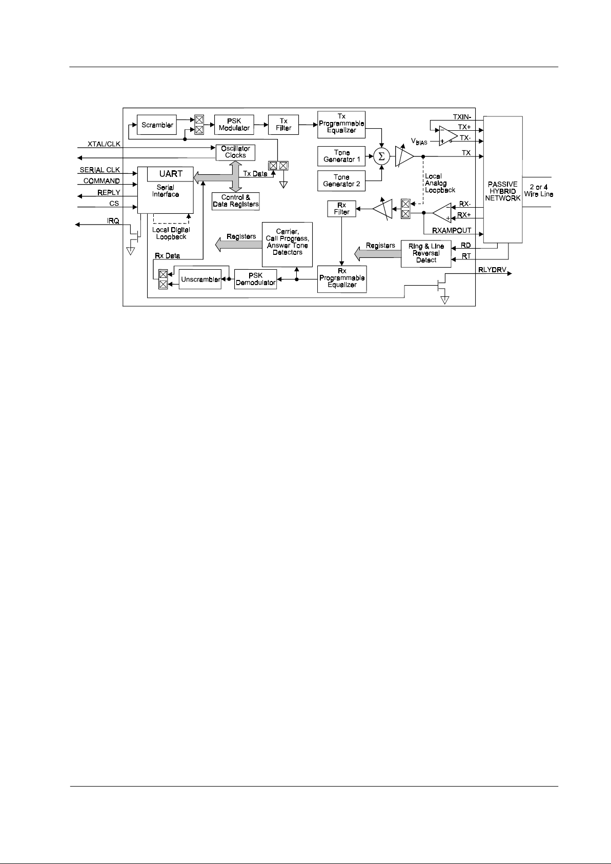
1 Block Diagram
Figure 1: Block Diagram
Bell 212A / V.22 Modem with Call Progress and DTMF 4 CMX644A Preliminary Information
2000 MX-COM, Inc. www.mxcom.com tel: 800 638 5577 336 744 5050 fax: 336 744 5054 Doc. # 20480197.006
4800 Bethania Station Road, Winston-Salem, NC 27105-1201 USA All trademarks and service marks are held by their respective companies.
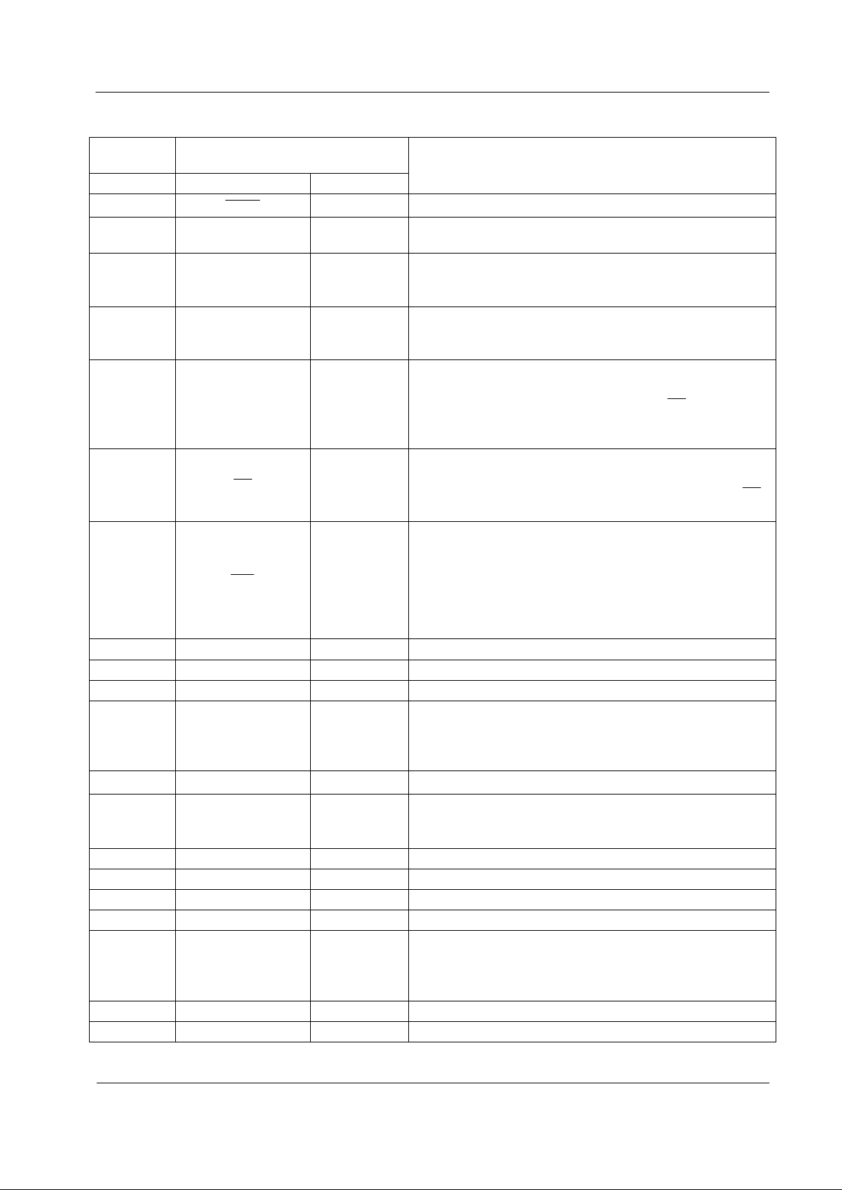
2 Signal List
CMX644A
D2/D5/P4
Signal
Pin No. Name Type
Description
1
XTAL
output The inverted output of the on-chip oscillator.
2 XTAL/CLOCK input
The input to the on-chip oscillator, for external Xtal circuit
or clock.
3 SERIAL CLOCK input
The ‘C-BUS’ serial clock input. This clock, produced by
the µController, is used for the transfer timing of
commands to and from the device.
4 COMMAND DATA input
The ‘C-BUS’ serial data input from the µController. Data
is loaded into this device in 8-bit bytes, MSB (B7) first,
and LSB (B0) last, synchronized to the SERIAL CLOCK.
5 REPLY DATA tri-state
The ‘C-BUS’ serial data output to the µController. The
transmission of REPLY DATA bytes is synchronized to
the SERIAL CLOCK under control of the
CS
input. This
3-state output is held at high impedance when not
sending data to the µController.
6
CS
input
Chip Select. The ‘C-BUS’ data loading control function:
this input is provided by the µController. Data transfer
sequences are initiated, completed or aborted by the
CS
signal.
7
IRQ
output
This output indicates an interrupt condition to the
µController by going to a logic ‘0’. This is a ‘wire-ORable’
output, enabling the connection of up to 8 peripherals to 1
interrupt port on the µController. This pin has a low
impedance pull-down to logic ‘0’ when active and a high
impedance when inactive. An external pull-up resistor is
required.
8 TX output The output of the transmit gain control.
9 TX+ output The output of the line driver amplifier.
10 TXIN- input The inverting input to the line driver amplifier.
11 TX- output
The inverted output of the line driving amplifier. Pins TX+
and TX- provide symmetrical outputs for use with a
balanced load to give sufficient Tx line signal levels even
at low V
DD
.
12
V
SS
power The negative supply rail (ground).
13
V
BIAS
output
A bias line for the internally circuitry, held at V
DD
/2. This
pin must be decoupled by a capacitor mounted close to
the device pins.
14 RLYDRV output An open-drain output for controlling a relay.
15 RX+ input The non-inverting input of the receive op-amp.
16 RX- input The inverting input of the receive op-amp.
17 RXAMPOUT output The output of the receive op-amp.
18 RT bi-directional
Open-drain output and Schmitt trigger input forming part
of the Ring or Line Polarity Reversal detector. An
external resistor to V
DD
and a capacitor to VSSshould be
connected to RT to filter and extend the RD input signal.
19 RD Input to the Ring or Line Polarity Reversal Detector.
20, 21, 22 - N/C No connections should be made to these pins.

Bell 212A / V.22 Modem with Call Progress and DTMF 5 CMX644A Preliminary Information
2000 MX-COM, Inc. www.mxcom.com tel: 800 638 5577 336 744 5050 fax: 336 744 5054 Doc. # 20480197.006
4800 Bethania Station Road, Winston-Salem, NC 27105-1201 USA All trademarks and service marks are held by their respective companies.
CMX644A
D2/D5/P4
Signal
Pin No. Name Type
Description
23 A/D CAP output
The reference voltage for the internal A to D of the
receiver. This pin must be decoupled by a capacitor
mounted close to the device pins.
24
V
DD
power
The positive supply rail. Levels and thresholds within the
device are proportional to this voltage. Should be
decoupled to V
SS
by a capacitor mounted close to the
device pins.
This device is capable of detecting and decoding small amplitude signals. It is recommended that the printed
circuit board be laid out with a ground plane in the CMX644A area to provide a low impedance connection
between the V
SS
pin and the VDDand V
BIAS
decoupling capacitors. The receive path should be protected as
much as possible from extraneous signals.
Table 1: Signal Lists
Bell 212A / V.22 Modem with Call Progress and DTMF 6 CMX644A Preliminary Information
2000 MX-COM, Inc. www.mxcom.com tel: 800 638 5577 336 744 5050 fax: 336 744 5054 Doc. # 20480197.006
4800 Bethania Station Road, Winston-Salem, NC 27105-1201 USA All trademarks and service marks are held by their respective companies.
3 External Components
1
C1
C2
C5
C4
R1
X1
XTAL
XTAL/CLOCK
C-BUS
to/from
µC
Tx Line
Interface.
See 5.1
Rx Line
Interface.
See 5.1
To/from R in g
Detector.
See 5.2
SERIAL CLOCK
COMMAND DATA
REPLY D ATA
CS
IRQ
TX
RX+
RLYDRV
Relay Drive
RX-
RXAMPOUT
RT
RD
V
DD
V
DD
TXIN-
TX+
TXV
SS
2
3
4
CMX644A
D5/D2/P4
5
6
7
8
9
10
11
12
13
14
15
16
17
18
19
20
21
22
23
24
V
BIAS
N/C
N/C
A/D CAP
N/C
C3
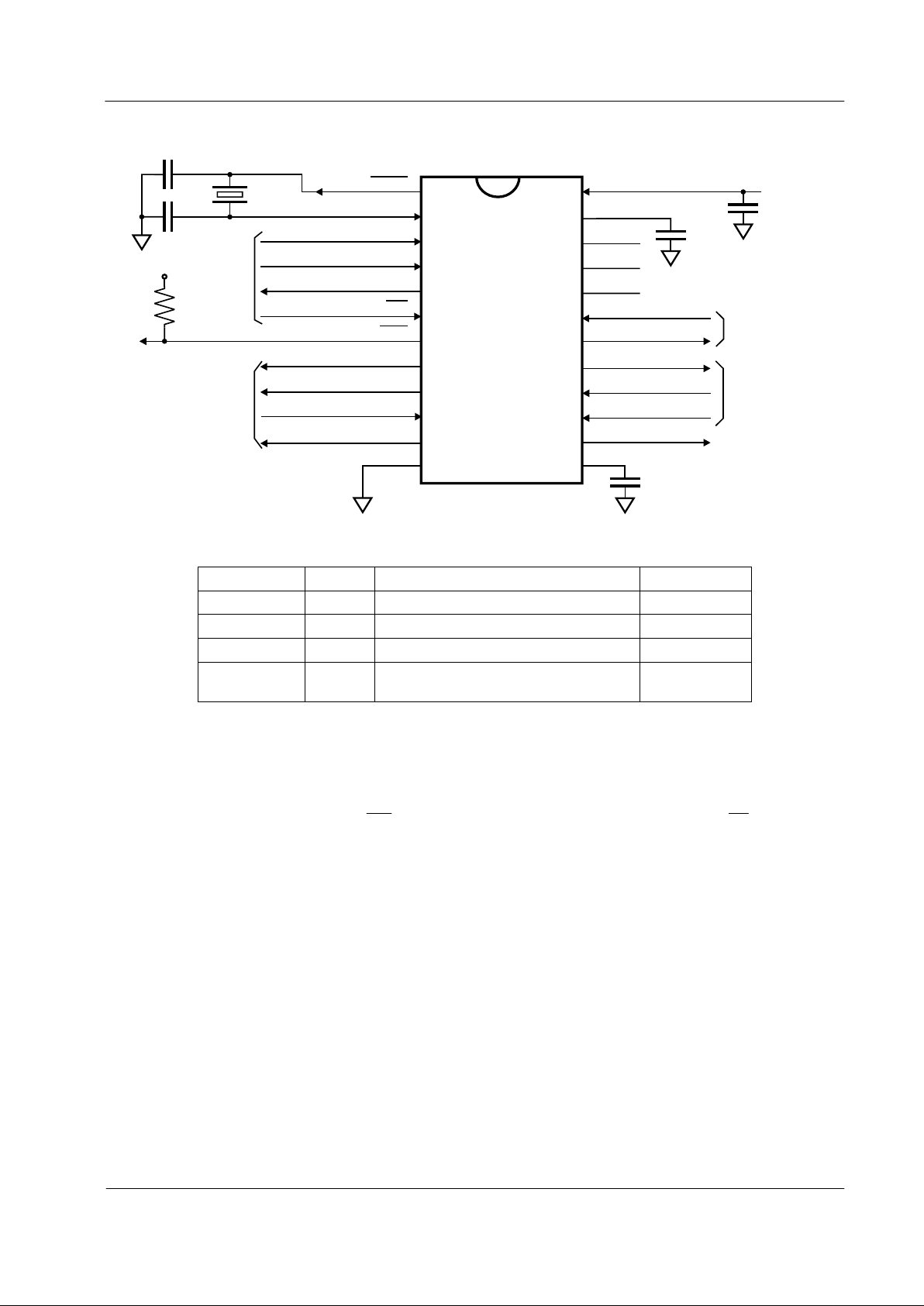
Figure 2: Recommended External Components
R1 Note 1
100kΩ±1%
C1, C2 18pF
±20%
C3, C4,
0.1µF ±20%
C5
1µF ±20%
X1 3.6864MHz, 7.372800MHz or
11.0592MHz
Tolerances for Resistors and Capacitors are as indicated unless otherwise stated.
Table 2: Recommended External Components for Typical Application
Recommended External Component Notes on Xtal Osc and Clock Dividers
1. R1 should be selected so that the
IRQ
pin has returned to its normal (high) state before
CS
pin goes
high.
2. Frequency and timing accuracy of the CMX644A is determined by the clock present at the XTAL/CLOCK
pin. This may be generated by the on-chip oscillator inverter using the external components C1, C2 and
X1 of Figure 2, or may be supplied from an external source to the XTAL/CLOCK input. If the clock is
supplied from an external source, C1, C2 and X1 should not be fitted.
3. The on-chip oscillator is turned off in the 'Zero-Power' mode.
4. If the clock is provided by an external source that is not always running, then the 'Zero-Power' mode must
be set when the clock is not available. Failure to observe this rule may cause a rise in the supply current
drawn by CMX644A.
5. For best results, a crystal oscillator design should drive the clock inverter input with signal levels of at
least 40% of V
DD
, peak to peak. Tuning fork crystals generally cannot meet this requirement. To obtain
crystal oscillator design assistance, please consult your crystal manufacturer.
Bell 212A / V.22 Modem with Call Progress and DTMF 7 CMX644A Preliminary Information
2000 MX-COM, Inc. www.mxcom.com tel: 800 638 5577 336 744 5050 fax: 336 744 5054 Doc. # 20480197.006
4800 Bethania Station Road, Winston-Salem, NC 27105-1201 USA All trademarks and service marks are held by their respective companies.
4 General Description
4.1 ‘C-BUS’ Serial Interface
This block provides for the transfer of data and control or status information between the CMX644A’s internal
registers and the µC over the ‘C-BUS’ serial bus. Each 'C-BUS' transaction consists of a single Register
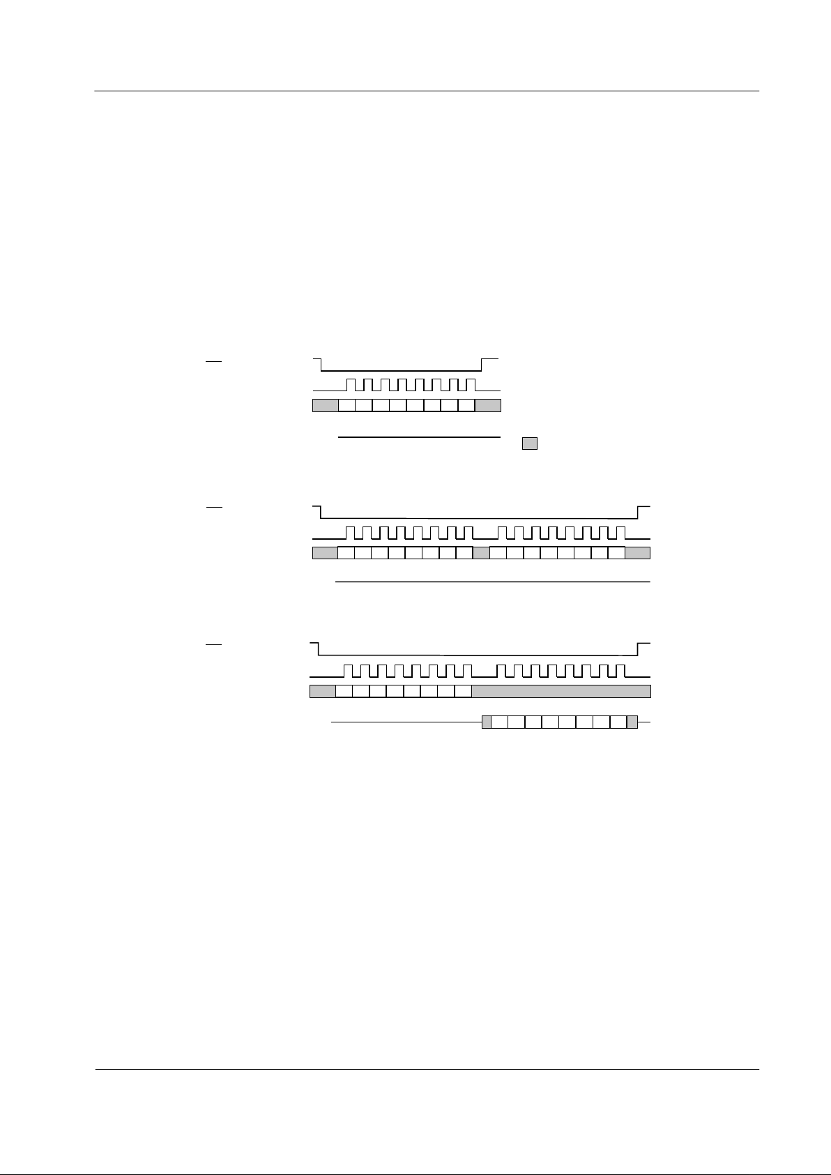
Address byte sent from the µC, as illustrated in Figure 3, which may be followed by either of:
1. A single data byte sent from the µC to be written into one of the CMX644A’s Write Only Registers, as
illustrated in Figure 4.
2. A single byte of data read out from one of the CMX644A’s Read Only Registers, as illustrated in Figure 5.
Data sent from the µC on the COMMAND DATA line is clocked into the CMX644A on the rising edge of the
SERIAL CLOCK input. REPLY DATA sent from the CMX644A to the µC is valid when the SERIAL CLOCK is
high. The interface is compatible with the most common µC serial interfaces such as SCI, SPI and Microwire,
and may be easily implemented with general purpose µC I/O pins controlled by a simple software routine.
See Figure 15 for detailed ‘C-BUS’ timing requirements.
CS
SERIAL CLOCK
COMMAND DATA
Address (01 Hex = Reset)
= Level not important
Hi-Z
REPLY DATA
7
654
321
0
Figure 3: C-BUS Transactions (Single byte from µµµµC)
CS
SERIAL CLOCK
COMMAND DATA
Address
Hi-Z
Data to CMX644A
REPLY DATA
7
654
321
0
7
654
321
0
Figure 4: C-BUS Transactions (One Address and one Data byte from µµµµC)
CS
SERIAL CLOCK
Hi-Z
Address
Data from CM X 6 4 4 A
COMMAND DATA
REPLY DATA
7
654
321
0
7
654
321
0
Figure 5: C-BUS Transactions (One Address byte from µµµµC and one Reply byte from CMX644A)
Bell 212A / V.22 Modem with Call Progress and DTMF 8 CMX644A Preliminary Information
2000 MX-COM, Inc. www.mxcom.com tel: 800 638 5577 336 744 5050 fax: 336 744 5054 Doc. # 20480197.006
4800 Bethania Station Road, Winston-Salem, NC 27105-1201 USA All trademarks and service marks are held by their respective companies.
4.2 UART
This block connects the µC, via the ‘C-BUS’ interface, to the received data from the PSK Demodulator and to
the transmit data input to the PSK Modulator.
As part of the UART function, this block can be programmed to convert data that is to be transmitted from
7 or 8-bit bytes to asynchronous data characters, adding Start and Stop bits, and - optionally - a parity bit to
the data before passing it to the PSK Modulator. In the receive direction the UART can extract data bits from
asynchronous characters coming from the PSK Demodulator, stripping off the Start and Stop bits, and
performing an optional Parity check on the received data, before passing the result, via the ‘C-BUS’, to the
µC. Bits 0-5 of the UART MODE Register control the number of Stop and Data bits and the Parity options for
both receive and transmit directions.
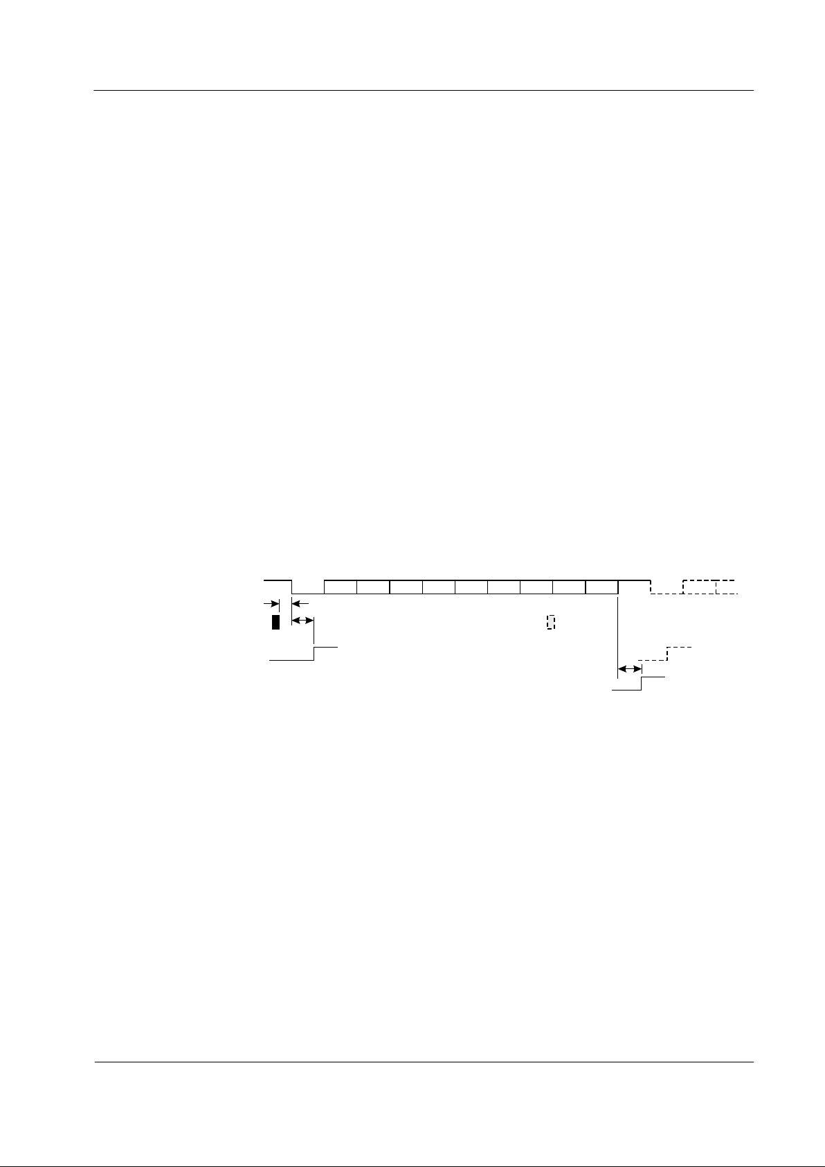
Data to be transmitted should be loaded by the µC into the TX DATA BYTE Register when the Tx Data Ready
bit (bit 1) of the FLAGS Register goes high. It will then be treated by the Tx UART block in one of two ways,
depending on the setting of bit 5 of the UART MODE Register:
1. If bit 5 of the UART MODE Register is ‘0’ (‘Sync’ mode) then the 8 bits from the TX DATA BYTE Register
will be transmitted sequentially LSB (D0) first.
2. If bit 5 of the UART MODE Register is ‘1’ (‘Async’ mode) then the 7 or 8 bits will be transmitted as
asynchronous data characters according to the following format:
One Start bit (Space).
7 or 8 Data bits from the TX DATA BYTE Register (D0-D6 or D0-D7) as determined by bit 0 of the
UART MODE Register. LSB (D0) transmitted first.
Optional Parity bit (even or odd parity) as determined by bits 1 and 2 of the UART MODE Register.
Zero, One or Two Stop bits (Mark) as determined by bits 3 and 4 of the UART MODE Register.
In both cases data will only be transmitted if bit 6 of the TX PSK MODE Register is set to ‘1’.
Failure to load the TX DATA BYTE Register with a new value when required will result in bit 2 (TX DATA
UNDERFLOW) of the FLAGS Register being set to ‘1’ and a continuous Mark (‘1’) signal will then be
transmitted until a new value is loaded into TX DATA BYTE Register.
TX DATA R egister loaded:
Tx DATA PSK signal:
t
DEL
t
LOAD
t
UFL
TX DATA READY flag bit:
TX DATA UNDERFLO W flag bit:
D0 D0
Start Start
P'ty
Stop
D1 D2
D3
D4
D5 D6
D7
Figure 6: Transmit UART Function (Async)
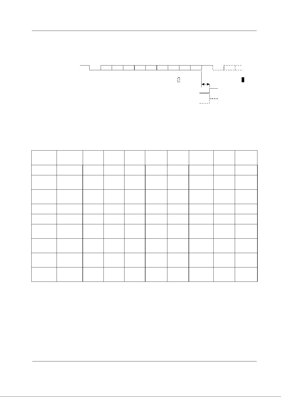
Received data from the PSK Demodulator goes into the receive part of the UART block, where it is handled in
one of two ways depending on the setting of bit 5 of the UART MODE Register:
1. If bit 5 of the UART MODE Register is ‘0’ (‘Sync’ mode) then the receive part of the UART block will
simply take 8 consecutive bits from the Demodulator and transfer them to the RX DATA BYTE Register
(the first bit going into the D0 position).
2. If bit 5 of the UART MODE Register is ‘1’ (‘Async’ mode) then the received data output of the PSK
Demodulator is treated as asynchronous characters each comprising:
A Start bit (Space).
7 or 8 Data bits as determined by bit 0 of the UART MODE Register. These bits will be placed into the
RX DATA BYTE Register with the first bit received going into the D0 position.
An optional Parity bit as determined by bits 1 and 2 of the UART MODE Register. If Parity is enabled
(bit 2 of the UART MODE Register = ‘1’) then bit 7 of the FLAGS Register will be set to ‘1’ if the
received parity is incorrect.
Any number of Stop bits (Mark).
Bell 212A / V.22 Modem with Call Progress and DTMF 9 CMX644A Preliminary Information
2000 MX-COM, Inc. www.mxcom.com tel: 800 638 5577 336 744 5050 fax: 336 744 5054 Doc. # 20480197.006
4800 Bethania Station Road, Winston-Salem, NC 27105-1201 USA All trademarks and service marks are held by their respective companies.
Bit 3 (RX DATA READY) of the FLAGS Register will be set to ‘1’ every time a new received value is loaded
into the RX DATA BYTE Register. If the previous contents of the RX DATA BYTE Register had not been read
out over the ‘C-BUS’ before the new value is loaded from the UART then bit 4 (RX DATA OVERFLOW) of the
FLAGS Register will also be set to ‘1’.
RX DAT A Register read:
Rx DATA PSK signal:
t
RDY
RX D ATA READY flag bit:
RX D ATA OV ERFLOW flag b it:
D0 D0
Start Start
P'ty
Stop
D1 D2
D3
D4
D5 D6
D7
Figure 7: Receive UART Function (Async)
The C-BUS serial clock should be fast enough to ensure that an RX DATA READY interrupt is serviced
completely within a time which is less than 8-bit times at 1200 baud, i.e. less than 6.67ms.
4.3 Software Description
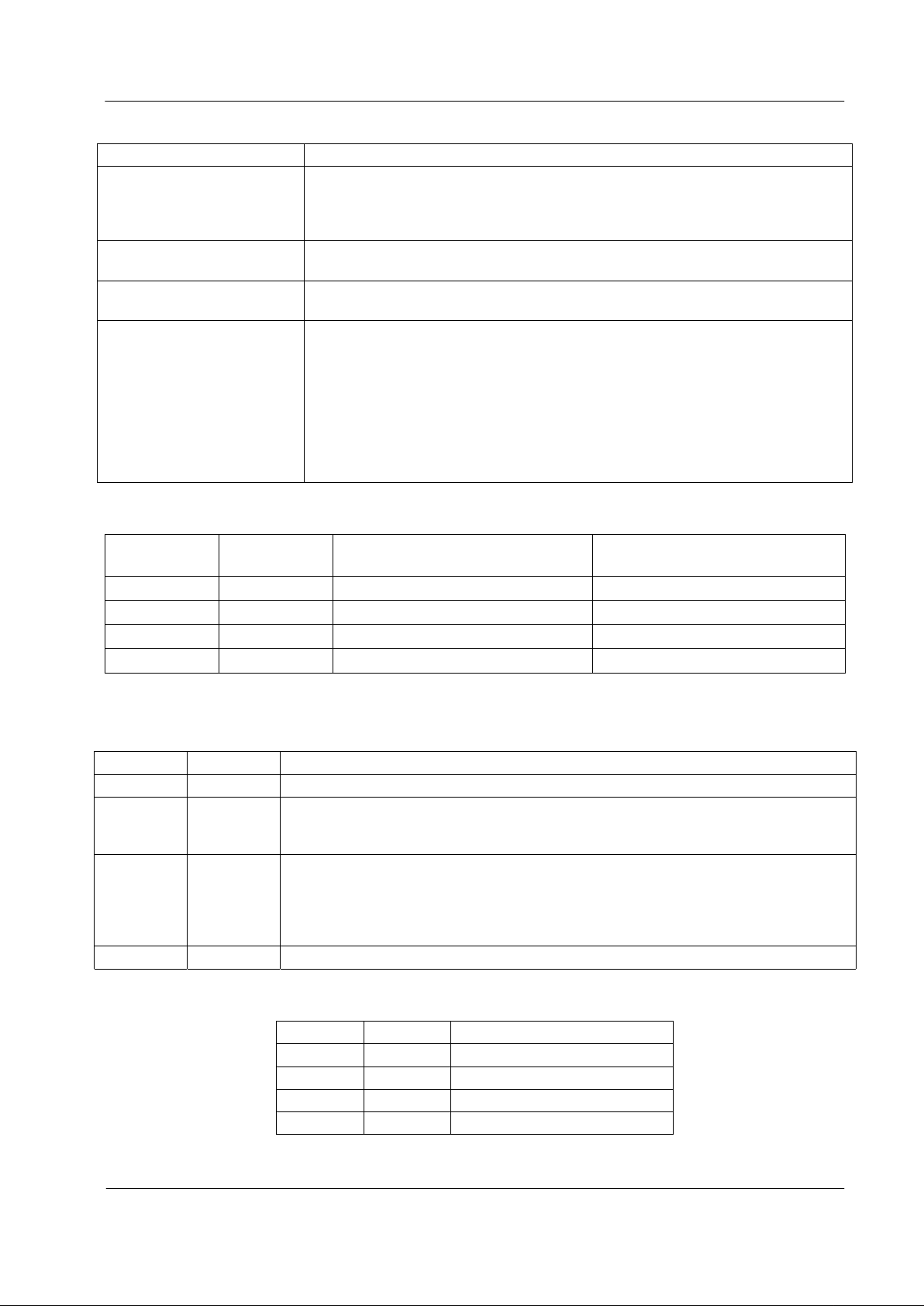
4.3.1 Write-only ‘C-BUS’ Registers
REGISTER
NAME
HEX
ADDRESS/
COMMAND
BIT 7
(D7)
BIT 6
(D6)
BIT 5
(D5)
BIT 4
(D4)
BIT 3
(D3)
BIT 2
(D2)
BIT 1
(D1)
BIT 0
(D0)
GENERAL
RESET
$01 N/A N/A N/A N/A N/A N/A N/A N/A
SET-UP $E0 0
RELAY
DRIVE
DETECT
DET1
DETECT
DET0
LOOPBACK:
L1
LOOPBACK:
L0
XTAL
FRQ:
X1
XTAL
FRQ:
X0
TX
TONES
$E1
TONE
SEL
TONE /
NOTONE
DTMF /
MODEM
TONES
DTMF /
SNGL
D3 D2 D1 D0
GAIN
BLOCKS
$E2
TXGAIN
TG3
TXGAIN
TG2
TXGAIN
TG1
TXGAIN
TG0
RXGAIN
RG3
RXGAIN
RG2
RXGAIN
RG1
RXGAIN
RG0
TX DATA
BYTE
$E3 D7 D6 D5 D4 D3 D2 D1 D0
UART
MODE
$E4 0 0
SYNC/
ASYNC
STOP
BITS
B
STOP
BITS
A
PARITY
ENABLE
PARITY
ODD/
EVEN
DATA
BITS
8/7
TX PSK
MODE
$E7 0
TX-
ENAB
SCRAMB
UNLOCK
SCRAMB
ENABLE
EQUAL
ET1
EQUAL
ET0
ENABLE
HI/LO
BAND
RX PSK
MODE
$E8 0
CPBW
SELECT
DESCRAMB
UNLOCK
DE-
SCRAMB
ENABLE
EQUAL
ER1
EQUAL
ER0
ENABLE
HI/LO
BAND
IRQ
MASK BITS
$EE
RX
PARITY
RING
DETECT
DETECT
RX DATA
OVER-
FLOW
RX
DATA
READY
TX DATA
UNDER-
FLOW
TX
DATA
READY
UN-
SCRAM
MARK
Table 3: Write only 'C-BUS' Register
4.3.2 Write-only Register Descriptions
4.3.2.1 GENERAL RESET ($01)
The reset command has no data attached to it. Application of the GENERAL RESET sets all write-only
register bits to ‘0’.
Bell 212A / V.22 Modem with Call Progress and DTMF 10 CMX644A Preliminary Information
2000 MX-COM, Inc. www.mxcom.com tel: 800 638 5577 336 744 5050 fax: 336 744 5054 Doc. # 20480197.006
4800 Bethania Station Road, Winston-Salem, NC 27105-1201 USA All trademarks and service marks are held by their respective companies.
4.3.2.2 SET-UP Register ($E0)
(Bit 7) Reserved for future use. This bit should be set to ‘0’.
RELAY DRIVE
(Bit 6)
This bit controls a low impedance pull-down transistor connected to the
RLYDRV pin to assist with the operation of an ‘off-hook relay’. When set to ‘1’
the transistor acts as a pull-down and will sink current. When set to ‘0’ the pin
is in a high impedance state.
DETECT DET1 and DET0
(Bits5and4)
These 2 bits control the operation of the receiver filter in order to facilitate the
detection of the following signals as shown in Table 5.
LOOPBACK L1 and L0
(Bits3and2)
These 2 bits control internal signal paths such that loopback tests can be
performed. Function is according to Table 6.
XTAL FRQ X1 and X0
(Bits1and0)
These two bits control the internal primary clock dividers to allow for a choice of
3 crystal frequencies. They can also be set to put the device into ‘Zero Power’
mode: in this mode all functions are powersaved, except for the ‘C-BUS’ and
the Ring Detector. In ‘Zero Power’ the crystal oscillator is disabled and the Bias
resistor chain is disconnected from the supplies.
Note: When the device is brought out of ‘Zero Power’ mode, the software
should allow at least 20ms for the crystal oscillator to re-start and for the Bias
capacitor to re-charge, before proceeding with any further device functions.
The function is provided according to Table 7.
Table 4: SET-UP Register ($E0)
DET1 (Bit 5) DET0 (Bit 4)
Required Rx HI/LO Band Setting
(Register $E8, Bit 0)
Detection Mode
0 0 As required for Rx PSK PSK Carrier
01LO='0' Call Progress
10HI='1' Answer Tone
1 1 As required for Rx PSK Detectors OFF
Note: RX PSK MODE register ENABLE bit should be set to '1' for answer tone and call progress detection.
Table 5: DETECT (DET1 and DET0)
L1 (Bit 3) L0 (Bit 2)
0 0 Normal Device Operation: no loopback.
01
Local Analog Loopback: the output of the Tx gain block is routed to the input of the
receiver gain block. (The connection between the receiver op-amp and gain block
is broken).
10
Local Digital Loopback: data is loaded into the TX DATA BYTE register in the usual
way via the ‘C-BUS’ when indicated by the TX DATA READY flag. This digital data
is internally retimed serially to the modem bit-rate and is then clocked into the
receiver buffer. When the receiver buffer is full the RX DATA READY flag will be set
and the data can then be read out of RX DATA BYTE register via the ‘C-BUS’.
1 1 Reserved for future use.
Table 6: LOOPBACK L1 and L0
X1 (Bit 1) X0 (Bit 0) Crystal / Mode
0 0 ‘Zero Power’
0 1 3.6864MHz crystal
1 0 7.3728MHz crystal
1 1 11.0592MHz crystal
Table 7: XTAL FREQ X1 and X0
 Loading...