DATA BULLETIN
Bell 202 and V.23 Modem
CMX624
with Call Progress and DTMF
PRELIMINARY INFORMATION
Features Applications
•
Bell 202 and V.23 Compatible Modem
•
1200bps Full duplex Operation (2 or 4 Wire)
•
Software Adjustable Tx and Rx Levels
•
Programmable Group Delay Equalizer
•
Answer/Originate Tone Generator/Detector
•
Call Progress Tone Detection
•
Integrated DTMF Encoder
•
Line Reversal and Ring Detector
•
Simple Serial Control Interface
•
Hook Switch Relay Driver
•
Zero-Power Standby Mode
•
3.0 to 5.0V Operation
Ring & Line
Reversal Detect
Transmit
Filter
µC
IRQ
CS
CLK
RXD
TXD
Serial
Interface
+
Tx/Rx Data
UART
Call Progress
and
Data Detect
FSK
De-modulator
FSK/DTMF
Modulator
Receive
Filter and
Equalizer
V
•
•
•
•
•
•
•
•
Xtal Osc and
Clock Dividers
BIAS
Telephone Telemetry Systems
Remote Utility Meter Reading
Security Systems
Payphones
Cable-TV Set Top Boxes
Industrial Control Systems
Electronic Cash Terminals
Vending Machines
RT
RD
XTAL/CLK
XTAL
RXRX+
RXAMPOUT
TXINTX+
TXTX
RLYDRV
Passive
Hybrid
Network
2 or 4
Wire Line
The CMX624 Bell 202 and V.23 modem provides full duplex 1200bps data signaling suitable for telephone
based information and telemetry systems where low power operation is desired. Bell 202 and V.23 signaling
delivers fast call set up times and robust, error resistant, transmission in 2 or 4 wire line circuits. A rich set of
important additional functions enhances end product value while reducing size. These include: integrated
DTMF encoder for dial out functions, single tone encoder for ‘melody’ generation, answer tone
generator/detector, line reversal and ring detector for ‘waking’ up a sleeping µC, adjustable Tx and Rx gain,
and a low impedance pull down output for hook relay control. The addition of the answer tone
generator/detector and call progress tone detector makes the set-up of a telephone call much easier for the
host µC to accomplish.
Very low power telemetry and data collection applications are supported by the CMX624’s ‘Zero Power’
standby mode in which the device will detect telephone line ringing voltage or line voltage reversal events.
Pin compatible with the CMX644A Bell212A / V.22 modem, the CMX624 is available in the following
packages: 24-pin SSOP (CMX624D5), 24-pin SOIC (CMX624D2), and 24-pin PDIP (CMX624P4).
1999 MX-COM, Inc. www.mxcom.com Tel: 800 638 5577 336 744 5050 Fax: 336 744 5054 Doc. # 20480180.108
4800 Bethania Station Road, Winston-Salem, NC 27105-1201 USA All trademarks and service marks are held by their respective companies.

Bell 202 and V.23 Compatible Modem 2 CMX624 Preliminary Information
CONTENTS
Section Page
1 Block Diagram................................................................................................................3
2 Signal List.......................................................................................................................4
3 External Components....................................................................................................5
4 General Description.......................................................................................................6
4.1 ‘C-BUS’ Serial Interface....................................................................................................... 6
4.2 Software Description ........................................................................................................... 7
4.3 Xtal Oscillator ...................................................................................................................... 8
4.4 Rx Input Amplifier ................................................................................................................ 8
4.5 Receive Filter....................................................................................................................... 8
4.6 Equalizer.............................................................................................................................. 8
4.7 FSK Demodulator................................................................................................................ 9
4.8 Rx Energy and 2100Hz Detector....................................................................................... 10
4.9 FSK / DTMF Modulator...................................................................................................... 10
4.9.1 V.23 mode (Bit 7 of SETUP register = ‘0’):...........................................................................10
4.9.2 Bell 202 mode (Bit 7 of SETUP register = ‘1’):.....................................................................11
4.10 Transmit Filter.................................................................................................................... 12
4.11 Transmit Output Buffer......................................................................................................12
4.12 Ring Signal Detector.......................................................................................................... 12
4.13 Tx/Rx UART ...................................................................................................................... 13
5 Application Notes ........................................................................................................15
5.1 Line Interface..................................................................................................................... 15
5.1.1 4-Wire Line Interface............................................................................................................15
5.1.2 2-Wire Line Interface............................................................................................................16
5.2 Ring Detector Interface......................................................................................................17
6 Performance Specification..........................................................................................19
6.1 Electrical Performance ...................................................................................................... 19
6.1.1 Absolute Maximum Ratings.................................................................................................. 19
6.1.2 Operating Limits...................................................................................................................19
6.1.3 Operating Characteristics.....................................................................................................20
6.1.4 Timing...................................................................................................................................24
6.2 Packaging.......................................................................................................................... 25
MX-COM, Inc. reserves the right to change specifications at any time and without notice.
1999 MX-COM, Inc. www.mxcom.com Tel: 800 638 5577 336 744 5050 Fax: 336 744 5054 Doc. # 20480180.108
4800 Bethania Station Road, Winston-Salem, NC 27105-1201 USA All trademarks and service marks are held by their respective companies.

Bell 202 and V.23 Compatible Modem 3 CMX624 Preliminary Information
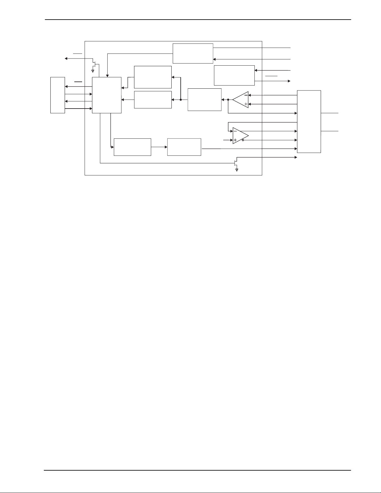
1 Block Diagram
RT
µC
IRQ
CS
CLK
RXD
TXD
Serial
Interface
+
Tx/Rx Data
UART
Call Progres s
Data Detect
De-modulator
FSK/DTMF
Modulator
Ring & Line
Reversal Detect
and
FSK
Transmit
Receive
Filter and
Equalizer
Filter
Figure 1: Block Diagram
Xtal Osc and
Clock Dividers
V
BIAS
RD
XTAL/CLK
XTAL
RXRX+
RXAMPOUT
TXINTX+
TX-
TX
RLYDRV
Passive
Hybrid
Network
2 or 4
Wire Line
1999 MX-COM, Inc. www.mxcom.com Tel: 800 638 5577 336 744 5050 Fax: 336 744 5054 Doc. # 20480180.108
4800 Bethania Station Road, Winston-Salem, NC 27105-1201 USA All trademarks and service marks are held by their respective companies.

Bell 202 and V.23 Compatible Modem 4 CMX624 Preliminary Information
2 Signal List
Pin No. Name Type Description
1
XTAL
2 XTAL/CLOCK input
3
SERIAL
CLOCK
4 COMMAND
DATA
5REPLY
DATA
6
7
CS
IRQ
8 TX output The Tx analog signal output.
9 TX+ output The output of the line driving amplifier.
10 TXIN- input The inverting input to the line driver amplifier.
11 TX- output The inverted output of the line driving amplifier.
12 V
13 V
SS
BIAS
14 RLYDRV output
15 RX+ input The non-inverting input to the Rx input amplifier.
16 RX- input The inverting input to the Rx input amplifier.
17 RXAMPOUT output The output of the Rx input amplifier.
18 RT bi-directional
19 RD input Schmitt trigger input to the Ring Signal Detector.
20 NC No connection should be made to this pin.
21 NC No connection should be made to this pin.
22 NC No connection should be made to this pin if the printed circuit
23 input No connection should be made to this pin if the printed circuit
24 V
DD
output The output of the on-chip Xtal oscillator inverter.
The input to the oscillator inverter from the Xtal circuit or
external clock source.
input
input
tri-state
The serial interface clock input from the µC. See Section 4.1
The serial interface data input from the µC.
A 3-state serial interface data output to the µC. This output is
high impedance when not sending data to the µC.
input
output
The serial interface transfer control input provided by the µC.
A ‘wire-ORable’ output for connection to a µC Interrupt Request
input. This output is pulled down to V
when active and is high
SS
impedance when inactive. An external pull-up resistor is
required.
Power The negative supply rail (ground).
output
Internally generated bias voltage of V
device is in ‘Zero Power’ mode when V
V
. Should be bypassed to VSS by a capacitor mounted close
SS
/2, except when the
DD
will discharge to
BIAS
to the device pins.
Relay drive open drain output. This output is pulled down to
V
when active and is high impedance when inactive.
SS
This pin is Bi-directional. An open drain output and Schmitt
trigger input forming part of the Ring Signal detector.
board is to be used for the CMX624 only. If the board is to be
used for the CMX644A, a capacitor should be connected as
shown in Figure 2.
board is to be used for the CMX624 only. If the board is to be
used for the CMX644A, a capacitor should be connected as
shown in Figure 2.
Power The positive supply rail. Levels and thresholds within the device
are proportional to this voltage. Should be bypassed to V
SS
by
a capacitor mounted close to the device pins.
Note: This device is capable of detecting and decoding small amplitude signals. To achieve this V
V
should be bypassed. It is very important to protect the receive path from extraneous in-band
BIAS
DD
and
signals. It is recommended that the printed circuit board be laid out with a ground plane in the
CMX624 area to provide a low impedance connection between the V
pin and the VDD and V
SS
BIAS
bypass capacitors.
1999 MX-COM, Inc. www.mxcom.com Tel: 800 638 5577 336 744 5050 Fax: 336 744 5054 Doc. # 20480180.108
4800 Bethania Station Road, Winston-Salem, NC 27105-1201 USA All trademarks and service marks are held by their respective companies.

Bell 202 and V.23 Compatible Modem 5 CMX624 Preliminary Information
3 External Components
C1
V
DD
C5
RD
RT
RXAMPOUT
RX-
RX+
RLYDRV
V
BIAS
C4
C3
To/fro m Ring
Detector.
See 5.2
Rx Line
Interface.
See 5.1
Relay Drive.
See 5.1
V
DD
R1
C2
C-BUS
to/from
µC
Tx Line
Interface.
See 5.1
X1
XTAL/CLOCK
SERIAL CLOCK
COMMAND DATA
REPLY DATA
XTAL
CS
IRQ
TX
TX+
TXIN-
TX-
V
SS
1
2
3
4
5
6
CMX624
7
D5/D2/P4
8
9
10
11
12
24
23
22
21
20
19
18
17
16
15
14
13
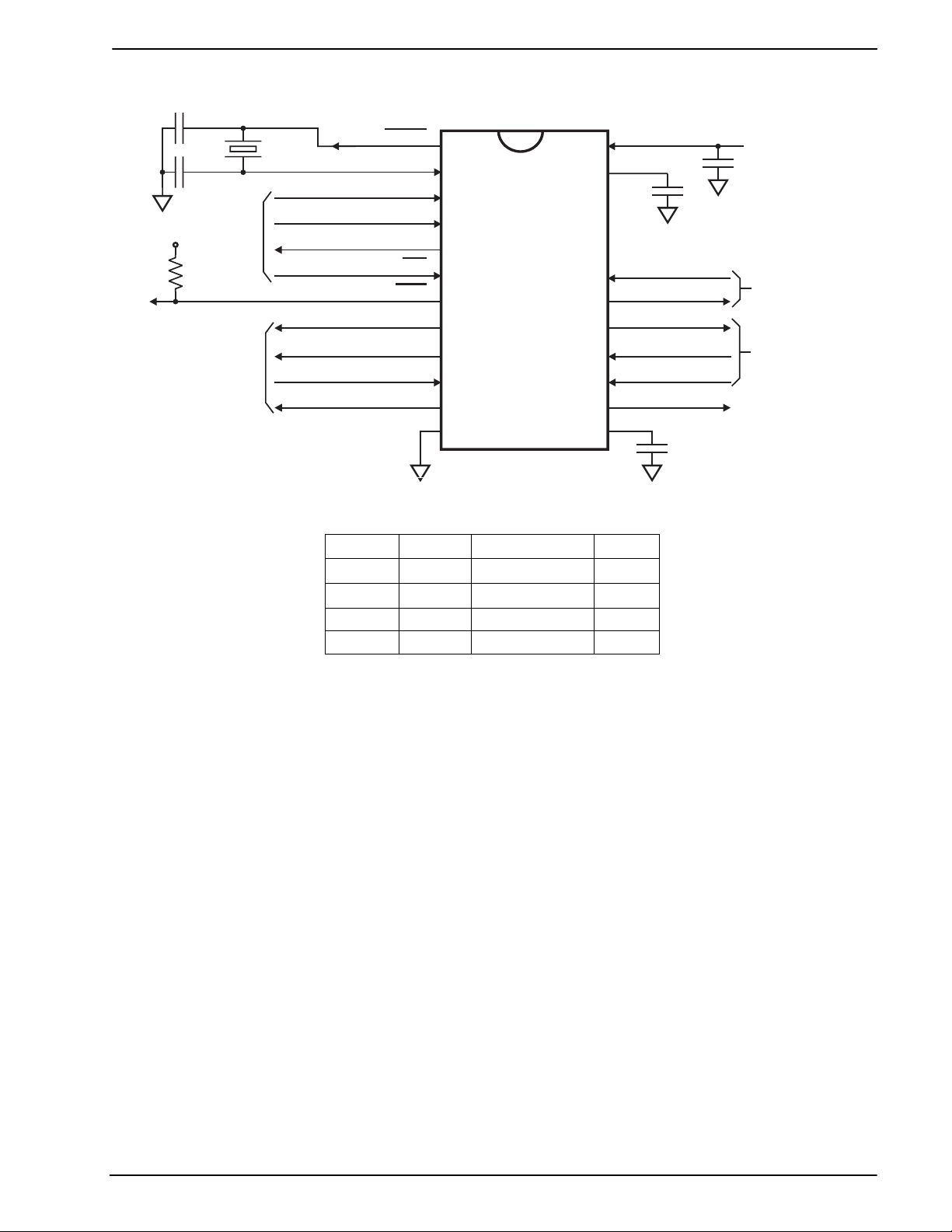
Figure 2: Recommended External Components
R1
C1, C2 18pF
C3, C4
C5 Note 1
X1 Note 2 3.579545MHz
Tolerances for Resistors and Capacitors are as indicated unless otherwise stated.
Table 1: Recommended External Components
Notes:
1. This component is only required for compatibility with CMX644A, see CMX644A Data Bulletin for
additional details.
2. For best results, a crystal oscillator design should drive the clock inverter input with signal levels of at
least 40% of V
crystal oscillator design assistance, please consult you crystal manufacturer.
, peak to peak. Tuning fork crystals generally cannot meet this requirement. To obtain
DD
Ω±
100k
0.1µF
±
10%
±
10%
5%,
1999 MX-COM, Inc. www.mxcom.com Tel: 800 638 5577 336 744 5050 Fax: 336 744 5054 Doc. # 20480180.108
4800 Bethania Station Road, Winston-Salem, NC 27105-1201 USA All trademarks and service marks are held by their respective companies.

Bell 202 and V.23 Compatible Modem 6 CMX624 Preliminary Information
4 General Description
The CMX624 contains a Bell 202 and V.23 compatible FSK modem. This device is capable of duplex
operation at 1200/75bps or 1200/150bps over a 2-wire line interface. It is also capable of 1200/1200bps over
a 4-wire line interface. This device also contains a flexible FSK data UART, a receive FSK or Call Progress
Tone energy detector, a 2100Hz detector, a DTMF generator, a Tx line driving buffer amplifier, a telephone
line Ringing Signal or Line Voltage Reversal detector and a 3.579545MHz Xtal oscillator. These functions are
controlled via a serial interface to the µC, which also carries the transmit and receive FSK modem data.
4.1 ‘C-BUS’ Serial Interface
This block provides for the transfer of data and control or status information between the CMX624’s internal
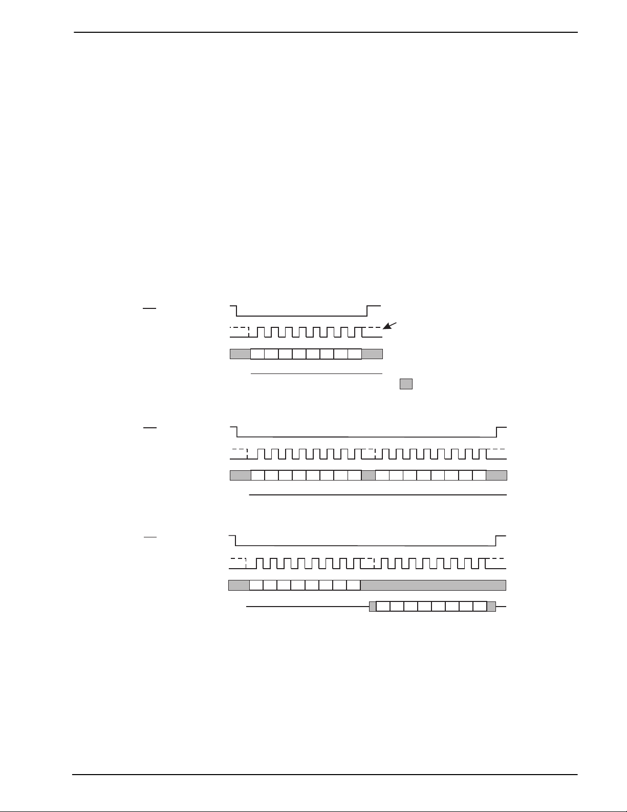
registers and the µC over the serial interface bus. Each ‘C-BUS’ transaction consists of a single Register
Address byte sent from the µC, as illustrated in Figure 3, which may be followed by either of:
1. A single data byte sent from the µC to be written into one of the CMX624’s Write Only Registers, as
illustrated in Figure 4.
2. A single byte of data read out from one of the CMX624’s Read Only Registers, as illustrated in Figure 5.
Data sent from the µC on the Command Data line is clocked into the CMX624 on the rising edge of the Serial
Clock input. Reply Data sent from the CMX624 to the µC is valid when the Serial Clock is high. The interface
is compatible with the most common µC serial interfaces such as SCI, SPI and Microwire, and may also be
easily implemented with general purpose µC I/O pins controlled by a simple software routine. See Figure 16
for detailed Serial Bus timing requirements.
CS
SERIAL CLOCK
COMMAND DATA
REPLY DATA
654
7
Address (01 Hex = Reset)
Hi-Z
321
0
Note:
The SERIAL CLOCK
line may be high or low at
the start and end of each
transaction.
= Level not important
Figure 3: Serial Bus Transaction (Single byte from µC)
CS
SERIAL CLOCK
COMMAND DATA
REPLY DATA
Hi-Z
654
7
Address
321
0
654
7
Data to CMX 6 2 4
321
0
Figure 4: Serial Bus Transactions (One Address and one Data byte from µC)
CS
SERIAL CLOCK
COMMAND DATA
REPLY DATA
Hi-Z
654
7
Address
321
0
654
7
Data from CMX624
321
0
Figure 5: Serial Bus Transactions (One Address byte from µC and one Reply byte from CMX624A)
1999 MX-COM, Inc. www.mxcom.com Tel: 800 638 5577 336 744 5050 Fax: 336 744 5054 Doc. # 20480180.108
4800 Bethania Station Road, Winston-Salem, NC 27105-1201 USA All trademarks and service marks are held by their respective companies.

Bell 202 and V.23 Compatible Modem 7 CMX624 Preliminary Information
4.2 Software Description
Command Data Byte Bits
AddrReg.76543210
$01 RESET
$E0 SETUP
$E1 TX
TONES
$E3 TX DATA
$E7 FSK
MODE
$EE
IRQ
MASK
FSK mode:
0 = V.23
1 = Bell 202
Tx Mode:
0 = FSK.
1 = Tones.
D7 D6 D5 D4 D3 D2 D1 D0
0 = Rx Sync
1 = Async
Reserved,
Set to 0
TX- output:
0 = Off
1 = On
Tone or
FSK output:
0 = Off.
1 = On.
Rx Equal:
0 = Off
1 = On
Reserved,
Set to 0
Relay Drive:
0 = o/c
1 = Pull low
Reserved,
set to 0
0 = Rx Call
Progress
1 = Rx FSK
Ring Detect
Change
Table 2: Write Only Serial Bus Register
AddrReg.76543210
$EA RX DATA
$EF FLAGS
** See note 2 and 3
D7 D6 D5 D4 D3 D2 D1 D0
Bad Rx
Parity
Ring Detect
Ring Detect
Change **
SINGLE BYTE COMMAND
0 = Zero
Power
1 = Normal
0 = DTMF
1 = Single
tone
0 = Rx 75 /
150bps
1 = RX1200
Reserved,
Set to 0
Stop bits:
0 = 1 bit
1 = 2 bits
Reserved,
set to 0
0 = Tx Sync
1 = Async
Rx Data
overflow
Reply Data Byte Bits
Rx Energy
or 2100Hz
detect.
Rx Data
overflow **
Parity:
0 = None
1 = Parity
Reserved,
set to 0
Tx output
level:
0 = Normal
1 = +3dB
Rx Data
ready
Rx Data
ready **
Parity:
0 = Odd
1 = Even
Reserved,
set to 0
FSK
Enable:
0 = Off
1 = On
(Tx & Rx)
Tx Data
underflow
Tx Data
underflow **
Data bits:
0 = 8 bits
1 = 7 bits
Set Detect:
0 = FSK/CP
1 = 2100Hz
0 = Tx 75 /
150bps
1 = 1200 or
DTMF
Tx Data
ready
Tx Data
ready **
Table 3: Read Only Serial Bus Registers
Notes:
1. Accessing the RESET Register over the Serial Bus clears all of the bits in the SETUP, TX TONES, TX
DATA, FSK MODE and IRQ MASK registers, and Bits 0-3 and Bit 5 of the FLAGS Register to ‘0’. This
will set the device into Zero Power mode.
a) This is a single-byte Serial Bus transaction consisting solely of the address byte value $01.
b) Placing the device in Zero Power mode by directly setting SETUP Bit 4 to ‘0’ does not clear the other
register bits. Care should be taken before re-enabling the device that the other bits are set so as to
prevent undesired transient operation. In particular, bit 6 of the TXTONES Register should be set to
‘0’ to prevent modulation of the transmitter output.
2. If any of Bits 0, 1, 2, 3 or 5 of the FLAGS Register is ‘1’ and the corresponding bit of the IRQ MASK
Register is also ‘1’ then the
output of the CMX624 will be pulled low.
IRQ
3. Bit 5 (Ring Detect Change) of the FLAGS Register is set on every ‘0’ to ‘1’ or ‘1’ to ‘0’ change of Bit 6
(Ring Detect).
4. Clearing Bit 4 of the SETUP Register puts the CMX624 into the Zero Power mode by turning off all blocks
except for the Serial Bus interface and Ring Detector circuit.
5. Reading the FLAGS Register clears the
output and also clears Bits 0, 1, 2, 3 and 5 of the FLAGS
IRQ
Register.
6. FLAGS Register (bit 4) is ‘1’ whenever Rx Energy or 2100Hz are present and ‘0’ when both signals are
absent. IRQ Mask Register (bit 40 is normally set to ‘0’, but can be set to ‘1’ to enable interrupts on the
output. In the latter case,
IRQ
will be continuously pulled to ’0’ while Rx Energy or 2100Hz are
IRQ
present. This may be useful for device evaluation purposes.
1999 MX-COM, Inc. www.mxcom.com Tel: 800 638 5577 336 744 5050 Fax: 336 744 5054 Doc. # 20480180.108
4800 Bethania Station Road, Winston-Salem, NC 27105-1201 USA All trademarks and service marks are held by their respective companies.

Bell 202 and V.23 Compatible Modem 8 CMX624 Preliminary Information
4.3 Xtal Oscillator
The frequency and timing accuracy of the CMX624 is determined by a 3.579545MHz clock signal input to the
XTAL/CLOCK pin. This may be generated by the on-chip oscillator inverter using the external components
C1, C2 and X1 or may be supplied from an external source to the XTAL/CLOCK input. See Figure 2. If the
clock is supplied from an external source, components C1, C2, and X1 should not be fitted.
The on-chip oscillator is disabled in the 'Zero-Power' mode.
If the clock is provided by an external source, which may not always be running, then the 'Zero-Power' mode
must be enabled when the clock is not available. Failure to observe this rule may cause an increase in the
supply current consumption by the CMX624.
4.4 Rx Input Amplifier
The Rx Input Amplifier, with suitable external components, is used to adjust the received signal to the correct
amplitude for the FSK receiver and Energy Detect circuits and may also form part of a 2-wire or 4-wire hybrid
circuit. See Section 5.1.
4.5 Receive Filter
This block includes a bandpass filter whose characteristics are set by Bits 4 and 5 of the FSK MODE Register
according to the receive operating mode (Call Progress, 75/150bps FSK or 1200bps FSK). It is used to
attenuate out of band noise and interfering signals; especially the locally generated transmit FSK signal that
could otherwise interfere with the received FSK signal when the modem is operating in 2-wire duplex mode.
4.6 Equalizer
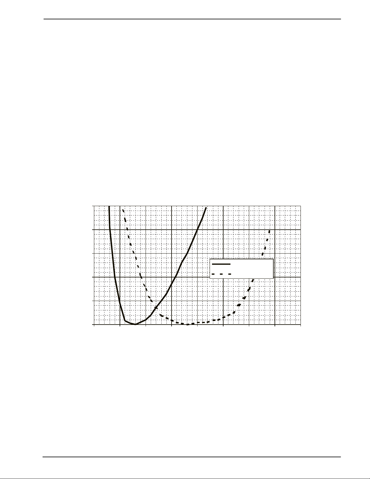
When receiving 1200bps FSK data an optional equalizer section can be enabled by setting Bit 6 of the FSK
MODE Register, compensates for one-half of the ETS Test Line 1 characteristics shown in Figure 6.
5
4
3
dB
ms
2
1
0
0 500 1000 1500 2000 2500 3000 3500 4000
Hz
Figure 6: ETS 300 114 Test Line 1 Characteristics (Normalized)
dB wrt 800Hz
ms wrt 1700Hz
1999 MX-COM, Inc. www.mxcom.com Tel: 800 638 5577 336 744 5050 Fax: 336 744 5054 Doc. # 20480180.108
4800 Bethania Station Road, Winston-Salem, NC 27105-1201 USA All trademarks and service marks are held by their respective companies.
 Loading...