DATA BULLETIN
CMX615
1999 MX-COM, Inc. www.mxcom.com tel: 800 638 5577 336 744 5050 fax: 336 744 5054 Doc. # 20480196.002
4800 Bethania Station Road, Winston-Salem, NC 27105-1201 USA All trademarks and service marks are held by their respective companies
Digital Line to
POTS Interface
PRELIMINARY INFORMATION
Features Applications
•
Pre-Programmed Tone Generators
•
Digital Line to POTS Interface
•
Fully Integrated DTMF Encoder
•
Subscriber Terminal Adapters
•
SPM Generator
•
Wireless Local Loop
•
Simple Serial Control Interface
•
Computer Telephony Integration
•
‘Zero-Power’ (1µA) Standby Mode
•
Telephone/Radio Patch Systems
•
3.58MHz Xtal/Clock
•
Pair Gain Systems
•
Bell 202 / V.23 FSK Generator
•
Billing/SPM Systems
•
Digital Ringing Voltage Generator
Codec
DC-to-DC
µC
CALLER ID
RING
DIAL
SLIC
AnalogTelephone Port
Digital LineCircuit
CMX615
The CMX615 is an integrated telecom tone generator and DTMF encoder designed for ISDN interfaces,
Wireless Local Loop and Analog to Digital Telephone Conversion systems. The tone generator covers an
extensive range of pre-programmed tones used in analog telephone systems (POTS). Three outputs are
provided: ‘Ringing signals’, ‘In-band tones or FSK data’, and ‘12kHz/16kHz Metering pulses’. Simple software
control facilitates the interface to a wide range of commonly used µCs and SLICs, enabling a comprehensive
analog telephone line presentation.
The DTMF encoder generates the appropriate DTMF tones for the POTS interface. DTMF tone pairs can be
encoded along with each tone singly or with other dual tone signals, such as those used in CIDCW systems
and ‘On Hook’ signaling systems.
Other tone standards supported are: Fax and Modem ‘answer’ and ‘originate’, ITU (CCITT) ‘R1’ and ‘R2’
signals, and sufficient tones for simple melody generation. Communication to and from the host µC is
performed by a ‘C-BUS’ serial interface, which is compatible with common serial interfaces such as: SCI, SPI,
and Microwire.
The CMX615 operates using a 2.7V to 5.5V supply and is available in the following packages: 16-pin SOIC
(CMX615D4) and 16-pin PDIP (CMX615P3).

Digital Line to POTS Interface 2 CMX615 Preliminary Information
1999 MX-COM, Inc. www.mxcom.com tel: 800 638 5577 336 744 5050 fax: 336 744 5054 Doc. # 20480196.002
4800 Bethania Station Road, Winston-Salem, NC 27105-1201 USA All trademarks and service marks are held by their respective companies
CONTENTS
Section Page
1 Block Diagram................................................................................................................3
2 Signal List.......................................................................................................................4
3 External Components....................................................................................................5
4 General Description.......................................................................................................6
4.1 Xtal Osc and Clock Dividers................................................................................................ 6
4.2 Uncommitted Amplifier ........................................................................................................6
4.3 Tone/FSK Encoder and Tone Encoder ............................................................................... 6
4.4 SPM Generator.................................................................................................................... 9
4.5 Tx Signal Control................................................................................................................. 9
4.6 Tx UART............................................................................................................................ 10
4.7 ‘C-BUS’ Interface............................................................................................................... 11
4.8 ‘C-BUS’ Registers.............................................................................................................. 12
5 Application Notes ........................................................................................................12
5.1 Telecom Tones.................................................................................................................. 13
6 Performance Specification..........................................................................................17
6.1 Electrical Performance ...................................................................................................... 17
6.1.1 Absolute Maximum Ratings.................................................................................................. 17
6.1.2 Operating Limits...................................................................................................................17
6.1.3 Operating Characteristics.....................................................................................................18
6.1.4 Timing...................................................................................................................................20
6.2 Packaging.......................................................................................................................... 21
MX-COM, Inc. reserves the right to change specifications at any time and without notice.

Digital Line to POTS Interface 3 CMX615 Preliminary Information
1999 MX-COM, Inc. www.mxcom.com tel: 800 638 5577 336 744 5050 fax: 336 744 5054 Doc. # 20480196.002
4800 Bethania Station Road, Winston-Salem, NC 27105-1201 USA All trademarks and service marks are held by their respective companies
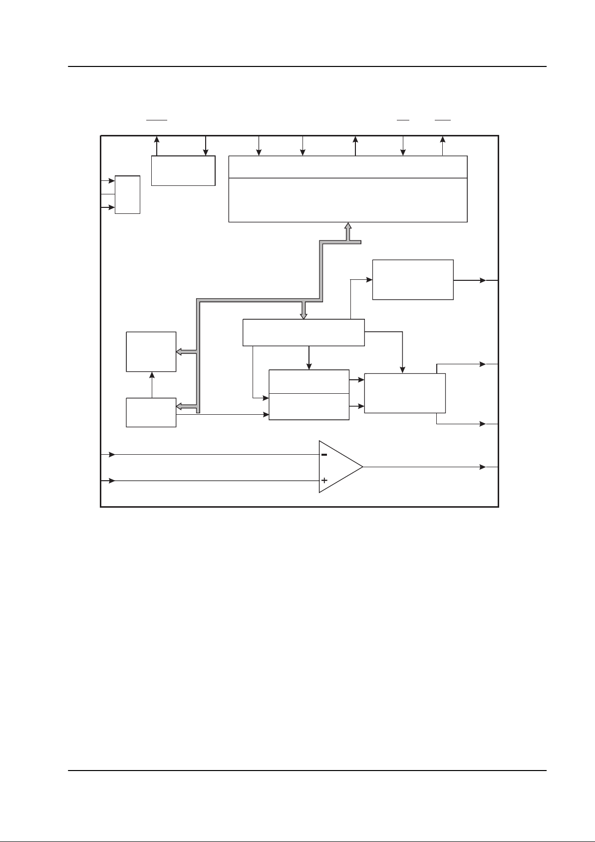
1 Block Diagram
V
DD
V
BIAS
V
SS
IN+
Tx UAR T
STATUS
and IRQ
BUS
3.58MHz
Oscillator
PSU
SPM Generator
XTAL
XTAL/CLOCK
SERIAL
CLOCK
COMMAND
DA T A
REPLY
DA T A
CS IRQ
C-BUS Computer Serial Portm
FSK/TONES
Tx Registers
SETUP and
MODE Registers
STATUS
Register
Interrupt
Generator
ROM
Tone Encoder
Tone/FSK
Encoder
Tx Signal
Control
SPM
RING
TONEFSK
AMPOUT
IN-
Figure 1: Block Diagram

Digital Line to POTS Interface 4 CMX615 Preliminary Information
1999 MX-COM, Inc. www.mxcom.com tel: 800 638 5577 336 744 5050 fax: 336 744 5054 Doc. # 20480196.002
4800 Bethania Station Road, Winston-Salem, NC 27105-1201 USA All trademarks and service marks are held by their respective companies
2 Signal List
CMX615
D4/P3
Signal Description
Pin No. Name Type
1
XTAL
output The output of the on-chip Xtal oscillator inverter.
2 XTAL/CLOCK input The input to the oscillator inverter from the Xtal circuit or
external clock source.
3 SERIAL
CLOCK
input
The ‘C-BUS’ serial clock input from the host µC.
See Section 4.8
4 COMMAND
DATA
input
The ‘C-BUS’ serial data input from the host µC.
5REPLY
DATA
tri-state
A 3-state ‘C-BUS’ serial data output to the host µC. This
output is high impedance when not sending data to the host
µ
C.
6
CS
input Chip Select. The ‘C-BUS’ transfer control input provided by
the host µC.
7
IRQ
output
A ‘wire-ORable’ output for connection to a host µC Interrupt
Request input. This output is pulled down to VSS when
active and is high impedance when inactive. An external
pull-up resistor is required.
8
V
SS
power The negative supply rail (ground).
9 TONEFSK output The sinewave output of the Tones and FSK signal
generators.
10 SPM output The sinewave output of the SPM signal generator.
11
V
BIAS
output
An internally generated bias voltage of V
DD
/2, except when
the device is in ‘Zero Power’ mode when V
BIAS
will
discharge to V
SS
. It should be bypassed to VSS by a
capacitor mounted close to the device pins.
12 IN+ input The non-inverting input to the uncommitted amplifier.
13 IN- input The inverting input to the uncommitted amplifier.
14 AMPOUT output The output of the uncommitted amplifier.
15 RING output The squarewave output of the Ringing Signal generator.
16
V
DD
power The positive supply rail. Levels within the device are
proportional to this voltage. It should be bypassed to V
SS
by a capacitor mounted close to the device pins.
It is recommended that the printed circuit board is laid out with a ground plane in the CMX615 area to
provide a low impedance connection between the V
SS
pin and the VDD and V
BIAS
bypass capacitors.
Table 1: Signal List

Digital Line to POTS Interface 5 CMX615 Preliminary Information
1999 MX-COM, Inc. www.mxcom.com tel: 800 638 5577 336 744 5050 fax: 336 744 5054 Doc. # 20480196.002
4800 Bethania Station Road, Winston-Salem, NC 27105-1201 USA All trademarks and service marks are held by their respective companies
3 External Components
16
15
14
13
12
11
10
9
1
2
3
4
5
6
7
8
XTAL/CLOCK
XTAL
IRQ
SERIAL CLOCK
REPLY DATA
COMMAND DATA
CS
RING
AMPOUT
IN-
V
BIAS
IN+
TONEFSK
X1
R1
C1
C2
C3
C4
V
SS
V
DD
V
DD
V
DD
CMX615
SPM
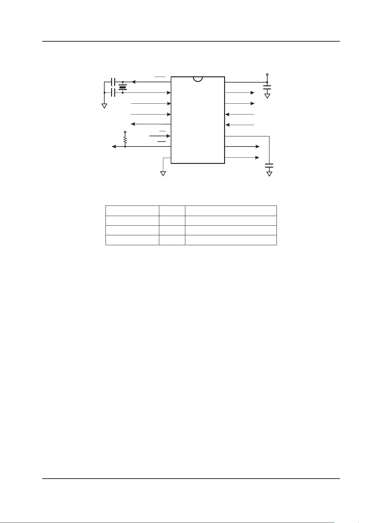
Figure 2: Recommended External Components
R1 100k
:
C1, C2 18pF
C3, C4 1.0µF
X1 3.579545 MHz
Resistors ±5%, capacitors ±10% unless otherwise stated.
Table 2: Recommended External Components
Recommended External Component Notes:
1. Resistors ±5%, capacitors ±10% unless otherwise stated.
2. For best results, a crystal oscillator design should drive the clock inverter input with signal levels of at
least 40% of V
DD
, peak to peak. Tuning fork crystals generally cannot meet this requirement. To obtain
crystal oscillator design assistance, please consult your crystal manufacturer.

Digital Line to POTS Interface 6 CMX615 Preliminary Information
1999 MX-COM, Inc. www.mxcom.com tel: 800 638 5577 336 744 5050 fax: 336 744 5054 Doc. # 20480196.002
4800 Bethania Station Road, Winston-Salem, NC 27105-1201 USA All trademarks and service marks are held by their respective companies
4 General Description
The CMX615 is a telecom tone generator and DTMF tone encoder. It has separate output ports for the three
different classes of signals encoded. These include Ringing signal, In-band tones or FSK data at 1200bps,
and High frequency metering pulses (SPM tones). It has a transmit level attenuator for In-band tones or FSK
data and an envelope control for SPM tones. It also has an uncommitted amplifier and uses the industry
standard 3.58MHz Xtal for its oscillator. These functions are controlled over a ‘C-BUS‘ serial µC interface,
which also carries the transmit FSK data.
The CMX615 may be powersaved into ‘Zero-Power’ mode for minimum power consumption by issuing a
‘C-BUS’ RESET command. Individual functions may be powersaved by the use of bits 6 and 7 in the SETUP
Register. Not powersaving the Tx Powersave (set bit 6 of the SETUP Register to ‘1’) will take the Tx
functions (tone/FSK encoding, DTMF, SPM and Ringing signal generation) out of powersave. Not
powersaving the Uncommitted Amplifier (Set bit 7 of the SETUP Register to ‘1’) will take the amplifier out of
powersave. Approximately 50ms should be allowed for the Tx DC level to settle at V
BIAS
before enabling the
Tx functions (set bit 6 of the MODE Register to ‘1’).
4.1 Xtal Osc and Clock Dividers
Frequency and timing accuracy of the CMX615 is determined by a 3.579545MHz clock present at the
XTAL/CLOCK pin. This may be generated by the on-chip oscillator inverter using the external components
C1, C2 and X1 of Figure 2, or may be supplied from an external source to the XTAL/CLOCK input. If the clock
is supplied from an external source, C1, C2 and X1 should not be fitted.
The on-chip oscillator is turned off in the 'Zero-Power' mode.
If the clock is provided by an external source, which is not always running, then the 'Zero-Power' mode must
be set when the clock is not available. Failure to observe this rule may cause a rise in the supply current
drawn by CMX615.
4.2 Uncommitted Amplifier
This amplifier, with suitable external components, can be used for adjusting the transmit signal level (for the
line hybrid).
4.3 Tone/FSK Encoder and Tone Encoder
When bit 5 of the MODE Register is set to ‘1’ then these blocks generate FSK signals as determined by bit 0
of the SETUP Register and the Tx data bits from the UART block, as shown in the table below:
SETUP Register Bit 0 Tone/FSK Generator FSK Signal Frequency
‘0’ (Space)
FSK Signal Frequency
‘1’ (Mark)
0 V23 1200bps FSK 2100Hz 1300Hz
1 Bell 202 1200bps FSK 2200Hz 1200Hz
Table 3: Tone/FSK Encoder and Tone Encoder
When bit 5 of the MODE Register is set to ‘0’, these blocks generate single or dual tones from the range
shown in Table 4, Table 5, Table 6, and Table 7 on the following pages. Bit 6 of the MODE Register is then
used to enable or disable the block’s output to the TX Signal Control, RING, and TONEFSK outputs. There
are four tone fields addressed by bits 0 and 1 of the MODE Register.

Digital Line to POTS Interface 7 CMX615 Preliminary Information
1999 MX-COM, Inc. www.mxcom.com tel: 800 638 5577 336 744 5050 fax: 336 744 5054 Doc. # 20480196.002
4800 Bethania Station Road, Winston-Salem, NC 27105-1201 USA All trademarks and service marks are held by their respective companies
TX TONES Register Bits 4-7 Frequency TX TONES Register Bits 0-3 Frequency
D7 D6 D5 D4 (Hz) D3 D2 D1 D0 (Hz)
0 0 0 0 0 = OFF 0 0 0 0 0 = OFF
0 0 0 1 252.4 0 0 0 1 * 17.1
0 0 1 0 268.7 0 0 1 0 * 20.5
0 0 1 1 285.3 0 0 1 1 * 24.9
0 1 0 0 315.5 0 1 0 0 * 34.1
0 1 0 1 330.5 0 1 0 1 * 41.0
0 1 1 0 375.2 0 1 1 0 * 51.2
0 1 1 1 404.3 0 1 1 1 1 0 0 0 468.0 1 0 0 0 262.9
1 0 0 1 495.8 1 0 0 1 293.6
1 0 1 0 520.6 1 0 1 0 348.2
1 0 1 1 548.0 1 0 1 1 392.6
1 1 0 0 562.8 1 1 0 0 1600
1 1 0 1 578.4 1 1 0 1 1633
1 1 1 0 595.0 1 1 1 0 1827
1 1 1 1 612.5 1 1 1 1 587.2
Table 4: Tone Field 0, MODE Register bit 1 and bit 0 = ‘0’ and ‘0’ respectively
NOTE: * These outputs are routed to the RING digital output instead of the TONEFSK output. Any single
tone output level at TONEFSK output is 0dBm.
TX TONES Register Bits 4-7 Frequency TX TONES Register Bits 0-3 Frequency
D7 D6 D5 D4 (Hz) D3 D2 D1 D0 (Hz)
0 0 0 0 0 = OFF 0 0 0 0 0 = OFF
0 0 0 1 120 0 0 0 1 330
0 0 1 0 150 0 0 1 0 416
0 0 1 1 154 0 0 1 1 420
0 1 0 0 250 0 1 0 0 425
0 1 0 1 300 0 1 0 1 433
0 1 1 0 350 0 1 1 0 440
0 1 1 1 360 0 1 1 1 450
1 0 0 0 367 1 0 0 0 460
1 0 0 1 375 1 0 0 1 480
1 0 1 0 380 1 0 1 0 500
1 0 1 1 383 1 0 1 1 600
1 1 0 0 400 1 1 0 0 620
1 1 0 1 450 1 1 0 1 720
1 1 1 0 475 1 1 1 0 930
1 1 1 1 480 1 1 1 1 -
Table 5: Tone Field 1, MODE Register bit 1 and bit 0 = ‘0’ and ‘1’ respectively
 Loading...