MX COM Inc CMX269AP6, CMX269AE2, CMX269AD3 Datasheet

DATA BULLETIN
CMX469A
1999 MX-COM, Inc. www.mxcom.com tel: 800 638 5577 336 744 5050 fax: 336 744 5054 Doc. # 20480191.002
4800 Bethania Station Road, Winston-Salem, NC 27105-1201 USA All trademarks and service marks are held by their respective companies.
1200/2400/4800bps
MSK Modem
PRELIMINARY INFORMATION
Features Applications
•
Selectable Data Rates
1200/2400/4800 bps
•
Full-Duplex MSK
•
RX and TX Bandpass Filters
•
Clock Recovery and Carrier Detect
Capabilities
•
Pin Selected Xtal/Clock Inputs
1.008MHz or 4.032MHz
•
Radio and General Applications
•
Data-Over-Radio
•
PMR/Cellular Signaling
•
Portable Data Terminals
•
Narrowband Coax Data Channels
•
Two Way Radio (MPT1327) Signaling
•
Personal/Cordless Telephone
The CMX469A is a full-duplex pin-selectable 1200/2400/4800bps Minimum Shift Key (MSK) Modem for FM
radio links. The mark and space frequencies are 1200/1800, 1200/2400, and 2400/4800Hz respectively.
Tone frequencies are phase continuous; transitions occur at the zero crossing point. The use of a common
Xtal oscillator with a choice of two clock frequencies (1.008MHz or 4.032MHz) provides data-rate, transmit
frequencies, and RX/TX synchronization. The transmitter and receiver operate entirely independently
including individual section powersave functions.
The CMX469A includes on-chip circuitry for Carrier Detect and RX Clock Recovery, both of which are made
available at output pins. RX, TX and Carrier Detect circuits contain bandpass filters to provide high quality
signals to their respective paths. The carrier detect time constant is set by an external capacitor, which may
be selected to optimize performance in high-noise environments.
High sensitivity and good bit-error-rate performance can be achieved even under adverse signal conditions.
The CMX469A operates with a 3.0V to 5.5V supply and is available in the following packages:
24-pin TSSOP (CMX469AE2), 20-pin SOIC (CMX469AD3), and 22-pin PDIP (CMX469AP6).

1200/2400/4800bps MSK Modem 2 CMX469A PRELIMINARY INFORMATION
1999 MX-COM, Inc. www.mxcom.com tel: 800 638 5577 336 744 5050 fax: 336 744 5054 Doc. # 20480191.002
4800 Bethania Station Road, Winston-Salem, NC 27105-1201 USA All trademarks and service marks are held by their respective companies.
Contents
Section Page
1. Block Diagram................................................................................................................3
2. Signal List.......................................................................................................................4
3. External Components....................................................................................................6
4. General Description.......................................................................................................7
4.1 Transmitter .......................................................................................................................... 7
4.2 Receiver .............................................................................................................................. 7
5. Application .....................................................................................................................8
5.1 Synchronous Modem Design Considerations ..................................................................... 8
5.2 Test Set Up.......................................................................................................................... 9
5.3 Bit Error Rate....................................................................................................................... 9
6. Performance Specifications........................................................................................11
6.1 Electrical Specifications..................................................................................................... 11
6.1.1 Absolute Maximum Limits.........................................................................................................11
6.1.2 Operating Limits .......................................................................................................................11
6.1.3 Operating Characteristics.........................................................................................................12
6.1.4 Timing.......................................................................................................................................14
6.2 Packages........................................................................................................................... 17
MX-COM, Inc. reserves the right to change specifications at any time without notice.

1200/2400/4800bps MSK Modem 3 CMX469A PRELIMINARY INFORMATION
1999 MX-COM, Inc. www.mxcom.com tel: 800 638 5577 336 744 5050 fax: 336 744 5054 Doc. # 20480191.002
4800 Bethania Station Road, Winston-Salem, NC 27105-1201 USA All trademarks and service marks are held by their respective companies.
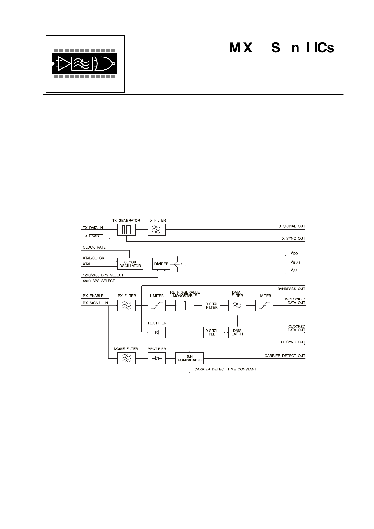
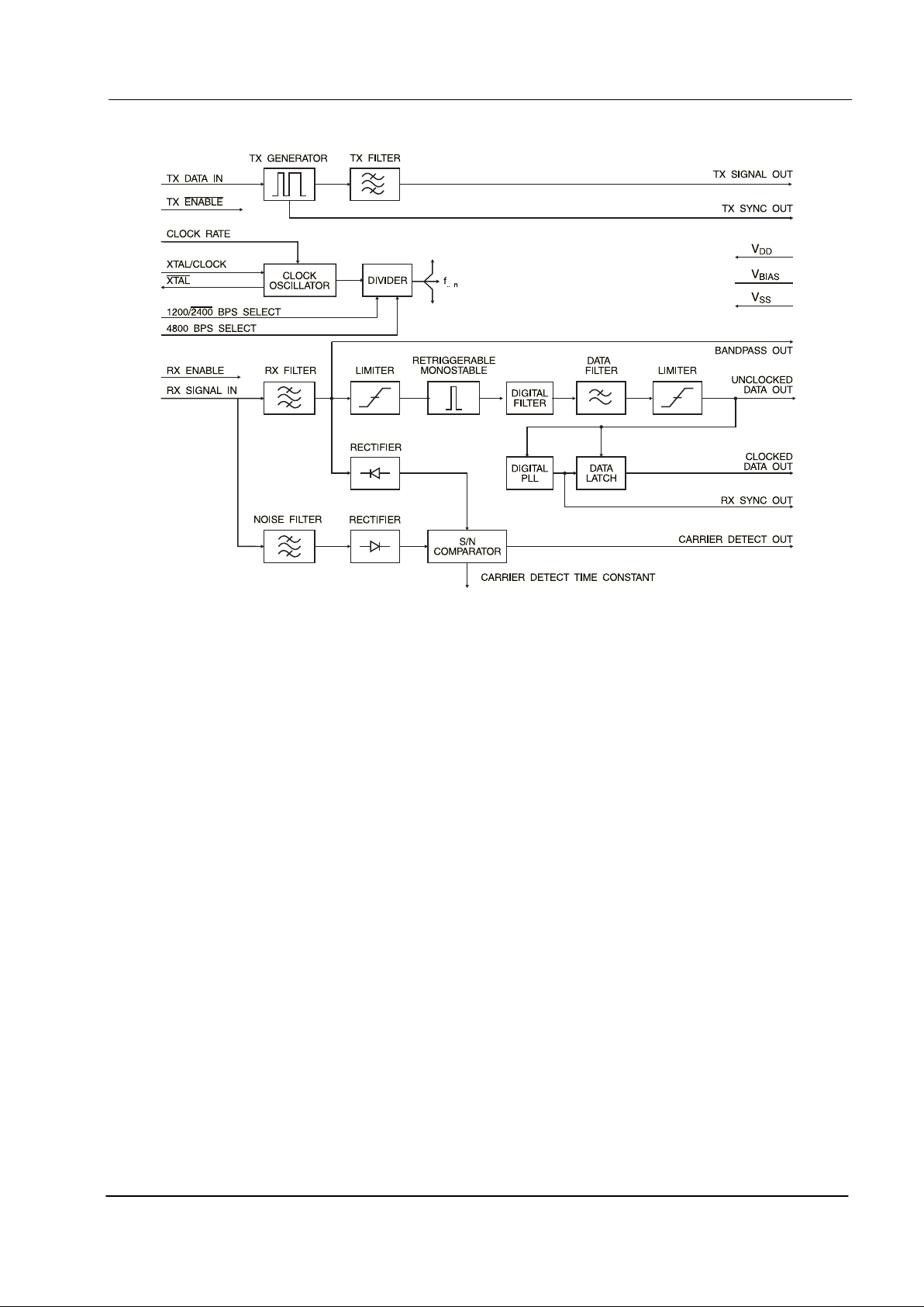
1. Block Diagram
Figure 1: Block Diagram

1200/2400/4800bps MSK Modem 4 CMX469A PRELIMINARY INFORMATION
1999 MX-COM, Inc. www.mxcom.com tel: 800 638 5577 336 744 5050 fax: 336 744 5054 Doc. # 20480191.002
4800 Bethania Station Road, Winston-Salem, NC 27105-1201 USA All trademarks and service marks are held by their respective companies.
2. Signal List
Pin No. Signal
E2 P6 D3 Name Type
Description
1 1 1 Xtal/Clock input
The input to the on-chip inverter, for use with either a
1.008MHz or a 4.032MHz Xtal or external clock.
Clock frequency selection is by the “Clock Rate”
input pin. The selection of this frequency will affect
the operational Data Rate of this device. Refer to
Table 3.
As specified in the Performance Specifications, this
input signal should be actively clocked (either driven
from an external source or via an XTAL circuit).
222
XTAL
output Output of the on-chip inverter.
3 3 3 TX Sync Out output
A squarewave, produced on-chip, to synchronize the
input of logic data and transmission of the MSK
signal. See Figure 8 and Section 4.1.
5 5 4 TX Signal Out output
When the transmitter is enabled, this pin outputs the
(140-step pseudo sinewave) MSK signal. See
Figure 8. With the transmitter disabled, this output is
set to a high-impedance state.
7 6 5 TX Data In input Serial logic data to be transmitted is input to this pin.
876
ENABLE TX
input
A logic ‘0’ will enable the transmitter. See Figure 8.
A logic ‘1’ at this input will put the transmitter into
powersave while forcing “TX Sync Out” to a logic ‘1’
and “TX Signal Out” to a high-impedance state. This
pin is internally pulled to V
DD
.
9 8 7 Bandpass Out output
The output of the RX Bandpass Filter. This output
impedance is typically 10kΩ and may require
buffering prior to use.
10 9 8 RX Enable input
The control of the RX function. The control of other
outputs is provided in Table 2
11 10 9
V
BIAS
power
The output of the on-chip analog bias circuitry. Held
internally at V
DD
/2, this pin should be bypassed to
V
SS
by a capacitor (C2). See Figure 2 and RX
Enable notes. This bias voltage is maintained under
all powersave conditions.
12 11 10 V
SS
power Negative supply (GND).
13 12 11
Unclocked
Data Out
output
The recovered asynchronous serial data output from
the receiver.
14 13 12
Clocked
Data Out
output
The recovered synchronous serial data output from
the receiver. Data is latched out by the recovered
clock, available at the “RX Sync Out”. See Figure 9
and Figure 11.
15 14 13 Carrier Detect output
When an MSK signal is being received this output is
a logic ‘1’.
16 15 14 RX Signal In input
The MSK signal input for the receiver. This input
should be coupled via a capacitor, C3.
18 17 15 RX Sync Out output
A flywheel squarewave output. This clock will
synchronize to incoming RX MSK data.
See Figure 9 and Figure 11.

1200/2400/4800bps MSK Modem 5 CMX469A PRELIMINARY INFORMATION
1999 MX-COM, Inc. www.mxcom.com tel: 800 638 5577 336 744 5050 fax: 336 744 5054 Doc. # 20480191.002
4800 Bethania Station Road, Winston-Salem, NC 27105-1201 USA All trademarks and service marks are held by their respective companies.
Pin No. Signal
E2 P6 D3 Name Type
Description
19 16 16
2400/1200
BPS Select
input
A logic ‘1’ on this pin selects the 1200bps option.
Tone frequencies are: one cycle of 1200Hz
represents a logic ‘1’, one-and-a-half cycles of
1800Hz represents a logic ‘0’.
A logic ‘0’ on this pin selects the 2400bps option.
Tone frequencies are: one-half cycle of 1200Hz
represents a logic ‘1’, one cycle of 2400Hz
represents a logic ‘0’. This pin has an internal 1M
Ω
pull-up resistor. Operational Data Rate
Configurations are illustrated in Table 3.
20 18 17
4800
BPS Select
input
A logic '1' on this pin combined with a logic '0' on the
2400/1200 BPS Select pin will select the 4800
option (1MΩ pulldown resistor). Tone frequencies
are: one-half cycle of 2400Hz represents a logic '1',
one full cycle of 4800Hz represents a logic '0'. This
state can only be achieved using a 4.032MHz Xtal
input. Operational Data Rate Configurations are
illustrated in Table 3.
21 19 18 Clock Rate input
A logic input to select and allow the use of either a
1.008MHz or 4.032MHz Xtal/clock. Logic ‘1’ =
4.032MHz, logic ‘0’ = 1.008MHz. This input has an
internal pulldown resistor (1.008MHz).
22 20 19
Carrier Detect
Time Constant
bi-directional
Part of the carrier detect integration function. The
value of C4 connected to this pin will affect the
carrier detect response time and therefore the noise
performance.
24 22 20 V
DD
power Positive supply. A single 2.7 to 5.0 volt supply is
required. This pin should be bypassed to V
SS
by a
capacitor (C5).
4, 6,
17, 23
4, 21 No internal connection, do not use.
Table 1: Signal List
RX Enable = RX Function Clock Data Output Carrier Detect Rx Sync Out
1 = Enabled Enabled * Enabled Enabled
0 = Powersave 0 1 or 0 1 or 0
* After enabling the receiver, a time of at least 8 bit periods, plus 2ms, should be allowed for
the Carrier Detect circuit to stabilize and provide a valid output.
Table 2: RX Enable Control Functions
XTAL/CLOCK Frequency 1.008MHz 4.032MHz
Clock Rate pin 00111
2400/1200 Select Pin
10100
4800 Select Pin 00001
Data Rate (bps) 1200 2400 1200 2400 4800
Table 3: Operational Data Rate Configuration

1200/2400/4800bps MSK Modem 6 CMX469A PRELIMINARY INFORMATION
1999 MX-COM, Inc. www.mxcom.com tel: 800 638 5577 336 744 5050 fax: 336 744 5054 Doc. # 20480191.002
4800 Bethania Station Road, Winston-Salem, NC 27105-1201 USA All trademarks and service marks are held by their respective companies.
3. External Components
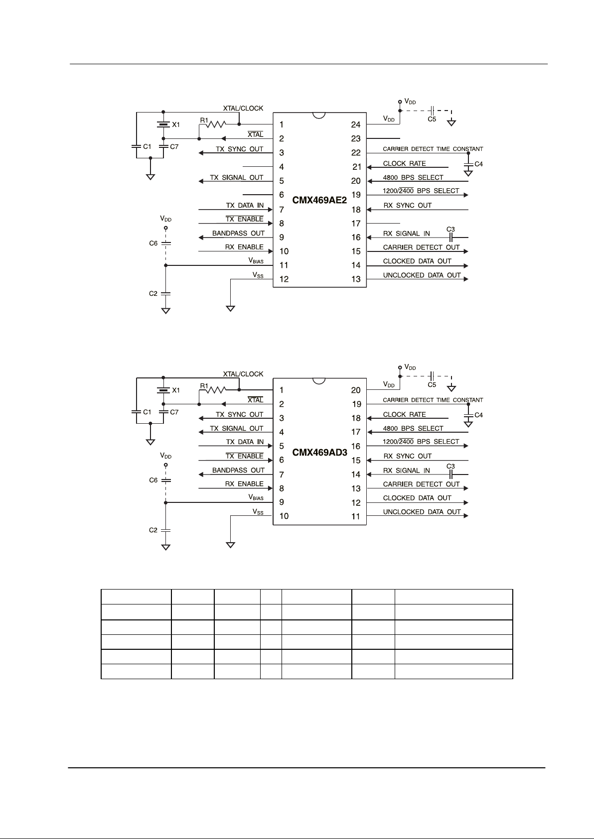
Figure 2: Recommended External Components for E2 package
Figure 3: Recommended External Components for D3 package
Component Notes Value Component Notes Value
R1
1.0M
Ω
C5 1.0µF
C1 33.0pF C6 1 1.0µF
C2 1 1.0µF C7 33.0pF
C3 0.1µF X1 3, 4, 5 1.008MHz or 4.032MHz
C4 2 0.1µF
Table 4: Recommended External Components
 Loading...