COMMUNICATION ICs
DATA BULLETIN
CMX264
Frequency Domain
Split-Band Scrambler
2000 MX-COM, Inc. www.mxcom.com tel: 800 638 5577 336 744 5050 fax: 336 744 5054 Doc. # 20480210.002
4800 Bethania Station Road, Winston-Salem, NC 27105-1201 USA All Trademarks and service marks are held by their respective companies.
ADVANCE INFORMATION
Features and Applications
•
Ensures Privacy
•
Full Duplex Operation
•
High Quality Recovered Audio
•
Low Height, Surface Mount Package
•
3.0V, Low Power Operation
•
Fixed or Rolling Code
•
Standby Mode
•
Uses Split Band Inversion
•
Low Current, Low Voltage
•
4.433619MHz Operation
MICIN
RXIN
V
SS
V
BIAS
V
DD
CLEAR
CLEAR
BIAS
BIAS
BIAS
XTAL
OSC
D E
D E
P E
XTAL
XTAL
MICO
EXTO
MUTERX
RECO
MUX
MUX
MUX
MUX
SCLK
SDATA
CS
SERIAL
PORT
CLOCK
GEN. &
CONTROL
fs
fs
fs
fs
TXLBIPF
RXLBIPF
TXLBOPF
RXLBOPF
TXUBIPF
TXUBOPF
RXUBIPF
RXUBOPF
fs
fs
fs
fs
BIAS
BIAS
P E
MUX
P E
MUX
P E
MUX
MUX
4.433619MHz
Xtal Pins
The CMX264 is a frequency domain scrambler for use in analog cellular phone systems. It contains separate
Tx and Rx paths for full duplex operation and operates under µProcessor control via a simple serial interface.
In the Tx path, scrambling is achieved by splitting the audio band into two parts, or sub-bands, and frequency
inverting each one. The frequency at which the signal is split, the “split-point”, can be either fixed or rolling
between four possible settings resulting in a transmitted audio signal which is unintelligible to eavesdroppers.
Descrambling is achieved by a receive device set to the same split point as the remote transmitter. Thus if
the Tx and Rx devices are synchronously cycled through the same sequence of split points, a clear recovered
signal will emerge at the output of the receiver.
A 4.433619MHz crystal is used allowing up to four split points to be programmed. The device is designed to
be compatible with existing cell-phone circuitry.
The CMX264 operates at 3.0V and is available in a 24-pin SSOP (CMX264D5).

Frequency Domain Split-Band Scrambler 2 CMX264 Advance Information
2000 MX-COM, Inc. www.mxcom.com tel: 800 638 5577 336 744 5050 fax: 336 744 5054 Doc. # 20480210.002
4800 Bethania Station Road, Winston-Salem, NC 27105-1201 USA All Trademarks and service marks are held by their respective companies.
CONTENTS
Section Page
1 Block Diagram................................................................................................................4
2 Signal List.......................................................................................................................5
3 External Components....................................................................................................6
4 General Description.......................................................................................................7
4.1 Tx Channel.......................................................................................................................... 7
4.1.1 Tx Channel Pre-Emphasis .....................................................................................................7
4.1.2 Tx Lowerband Input Filter (TXLBIPF).....................................................................................7
4.1.3 Tx Lowerband Balanced Modulator........................................................................................7
4.1.4 Tx Lowerband Output Filter (TXLBOPF)................................................................................7
4.1.5 Tx Upperband Input Filter (TXUBIPF)....................................................................................7
4.1.6 Upperband Balanced Modulator.............................................................................................7
4.1.7 Tx Upperband Output Filter (TXUBOPF) ...............................................................................8
4.1.8 Tx Summer.............................................................................................................................8
4.1.9 Tx Channel De-Emphasis ......................................................................................................8
4.2 Rx Channel.......................................................................................................................... 8
4.2.1 Rx Channel Pre-Emphasis.....................................................................................................8
4.2.2 Rx Lowerband Input Filter (RXLBIPF)....................................................................................8
4.2.3 Rx Lowerband Balanced Modulator.......................................................................................8
4.2.4 Rx Lowerband Output Filter (RXLBOPF)...............................................................................8
4.2.5 Rx Upperband Input Filter (RXUBIPF)...................................................................................8
4.2.6 Rx Upperband Balanced Modulator.......................................................................................8
4.2.7 Rx Upperband Output Filter (RXUBOPF)...............................................................................9
4.2.8 Rx Summer ............................................................................................................................9
4.2.9 Rx Channel De-Emphasis......................................................................................................9
4.3 Serial Interface .................................................................................................................... 9
4.3.1 General Operation..................................................................................................................9
4.3.2 Powersave Mode (D10)..........................................................................................................9
4.3.3 Clear/Scramble Modes (D9)...................................................................................................9
4.3.4 Output Select (D8, D7, D6) ..................................................................................................10
4.3.5 Pre/De-Emphasis Select (D5, D4, D3, D2) ..........................................................................11
4.3.6 Scramble Mode - Split Point Selection (D1, D0) ..................................................................11
5 Application Notes ........................................................................................................ 11
5.1 General Use ...................................................................................................................... 11
5.2 Input Anti-Alias and Output Smoothing Filters................................................................... 12
5.2.1 Input Anti-Alias Filtering .......................................................................................................12
5.2.2 Output Smoothing ................................................................................................................12

Frequency Domain Split-Band Scrambler 3 CMX264 Advance Information
2000 MX-COM, Inc. www.mxcom.com tel: 800 638 5577 336 744 5050 fax: 336 744 5054 Doc. # 20480210.002
4800 Bethania Station Road, Winston-Salem, NC 27105-1201 USA All Trademarks and service marks are held by their respective companies.
6 Performance Specification.......................................................................................... 12
6.1 Electrical Performance ...................................................................................................... 12
6.1.1 Absolute Maximum Ratings..................................................................................................12
6.1.2 Operating Limits...................................................................................................................12
6.1.3 Operating Characteristics.....................................................................................................13
6.2 Packaging.......................................................................................................................... 22
MX-COM, Inc. reserves the right to change specifications at any time and without notice.

Frequency Domain Split-Band Scrambler 4 CMX264 Advance Information
2000 MX-COM, Inc. www.mxcom.com tel: 800 638 5577 336 744 5050 fax: 336 744 5054 Doc. # 20480210.002
4800 Bethania Station Road, Winston-Salem, NC 27105-1201 USA All Trademarks and service marks are held by their respective companies.
1 Block Diagram
MICIN
RXIN
V
SSVBIAS
V
DD
CLEAR
CLEAR
BIAS
BIAS
BIAS
XTAL
OSC
D E
D E
P E
XTAL
XTAL
MICO
EXTO
MUTERX
RECO
MUX
MUX
MUX
MUX
SCLK
SDATA
CS
SERIAL
PORT
CLOCK
GEN. &
CONTROL
fs
fs
fs
fs
TXLBIPF
RXLBIPF
TXLBOPF
RXLBOPF
TXUBIPF
TXUBOPF
RXUBIPF
RXUBOPF
fs
fs
fs
fs
BIAS
BIAS
P E
MUX
P E
MUX
P E
MUX
MUX
4.433619MHz
Xtal Pins
Figure 1: Block Diagram

Frequency Domain Split-Band Scrambler 5 CMX264 Advance Information
2000 MX-COM, Inc. www.mxcom.com tel: 800 638 5577 336 744 5050 fax: 336 744 5054 Doc. # 20480210.002
4800 Bethania Station Road, Winston-Salem, NC 27105-1201 USA All Trademarks and service marks are held by their respective companies.
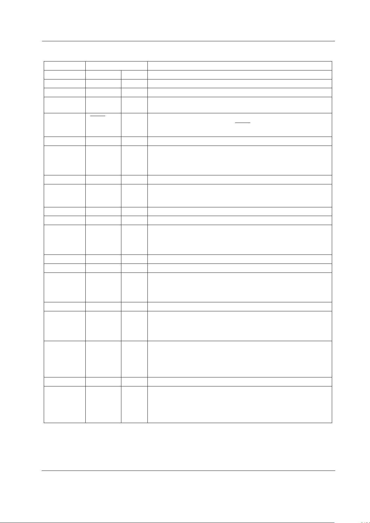
2 Signal List
Packages Signal Description
Pin No. Name Type
1 N/C This pin should be left unconnected.
2 N/C This pin should be left unconnected.
3 XTAL input A 4.433619MHz crystal is connected to these pins with the
appropriate external components (see Figure 2).
4
XTAL
output Alternatively, an externally derived clock signal may be applied to
the XTAL pin. In this case, the
XTALpin should be left
unconnected.
5 N/C This pin should be left unconnected.
6 MICO output The Tx audio output from the scrambler. This signal may be
scrambled or clear. If scrambled it may come from the variable
split-band (VSB) scrambler direct or via the Tx de-emphasis block.
All signal paths depend upon the internal state selected.
7 N/C This pin should be left unconnected.
8 V
BIAS
output A bias line for the internal circuitry, internally held at VDD/2. This
pin must be decoupled to V
SS
by a capacitor mounted close to the
device pins.
9 N/C This pin should be left unconnected.
10 N/C This pin should be left unconnected.
11 MICIN input The input for the signal from the microphone amplifier/limiter. This
pin may be the input to the Tx pre-emphasis circuit, the VSB
scrambler or the clear path, depending upon the internal state
selected.
12 VSS power The negative supply rail (ground)
13 N/C This pin should be left unconnected.
14 RXIN input The input for the received audio signal, whether scrambled or
clear. This pin may be routed to the Rx pre-emphasis circuit, the
flatband frequency descrambler or the clear path, according to the
internal state selected via the serial interface.
15 N/C This pin should be left unconnected.
16 MUTERX input A logic input which when high (VDD) immediately de-activates the
two Rx outputs (RECO and EXTO), overriding the serial data
previously loaded. When this input is low (V
SS
), the Rx outputs are
controlled by the serial data port.
17 EXTO output One of two Rx outputs. This is used for routing the recovered
audio to external devices, e.g. a speakerphone. This output may
be independently activated or de-activated by selecting the
appropriate internal state. When de-activated, either by the serial
data or by the MUTERX pin, the output is set to V
BIAS
.
18 N/C This pin should be left unconnected.
19 RECO output The other Rx output. This is used for routing the recovered audio
to the telephone loudspeaker. This output may be independently
activated or de-activated by selecting the appropriate internal
state. When de-activated, either by the serial data or by the
MUTERX pin, the output is set to V
BIAS
.

Frequency Domain Split-Band Scrambler 6 CMX264 Advance Information
2000 MX-COM, Inc. www.mxcom.com tel: 800 638 5577 336 744 5050 fax: 336 744 5054 Doc. # 20480210.002
4800 Bethania Station Road, Winston-Salem, NC 27105-1201 USA All Trademarks and service marks are held by their respective companies.
Packages Signal Description
Pin No. Name Type
20 NC This pin should be left unconnected.
21
CS
input
22 SCLOCK input
23 SDATA input
The serial port input pins. Data applied here sets up the internal
state of the device, e.g. split point, scramble/clear, etc.
See Figure 10.
24 VDD power The positive supply rail. This pin must be decoupled to VSS by a
capacitor mounted close to the device.
Table 1: Signal List
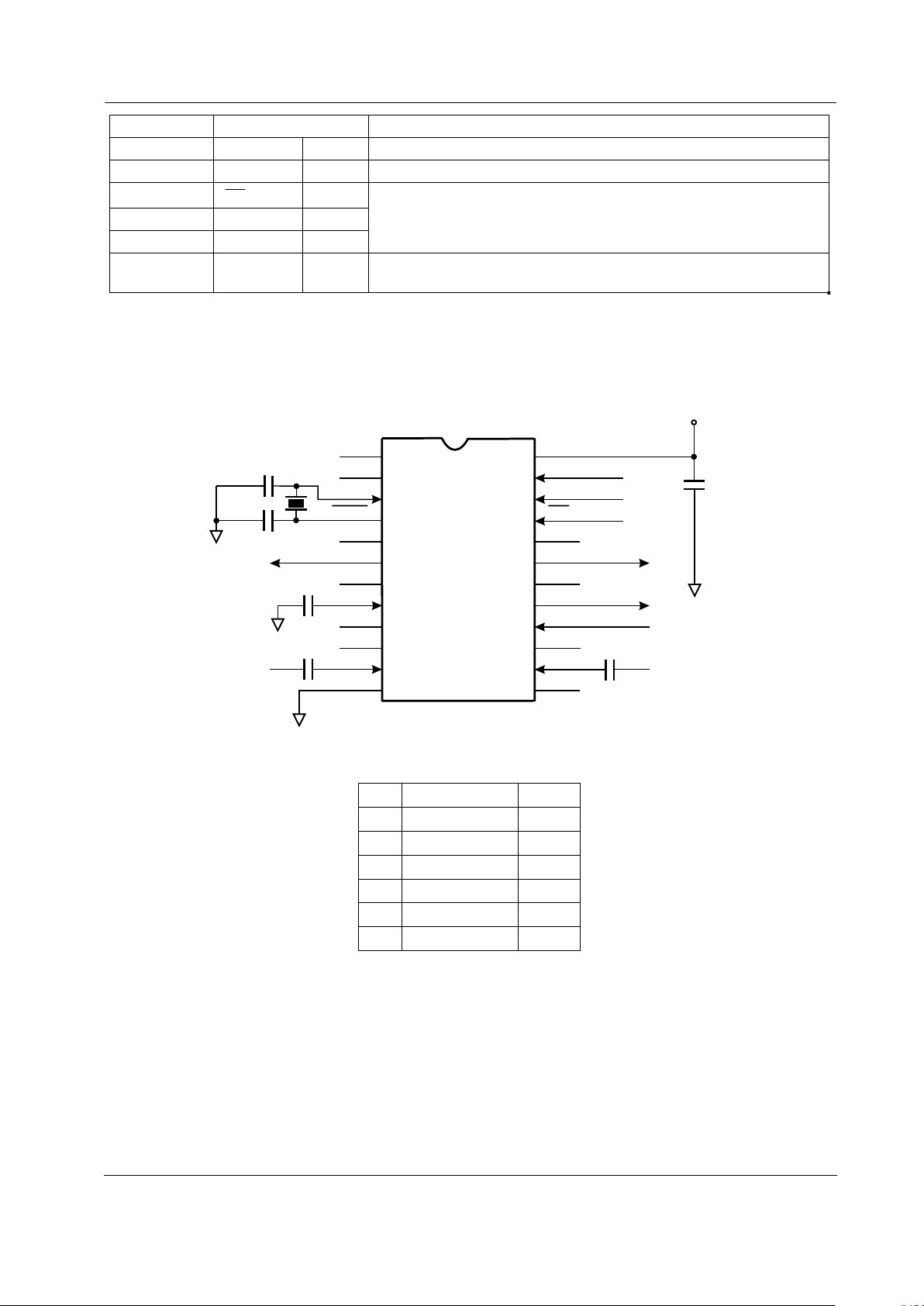
3 External Components
V
DD
V
SS
V
BIAS
XTAL
XTAL
X1
RECO
CMX264D5
EXTO
CS
RXIN
C4
C5
C6
C1
C2
C3
SDATA
SCLOCK
1
2
3
4
5
6
8
9
10
11
12 13
14
7
24
23
22
21
20
19
18
17
16
15
MICO
MUTERX
MICIN
N/C
N/C
N/C
N/C
N/C
N/C
N/C
N/C
N/C
N/C
V
DD
Figure 2: Recommended External Components
C1 10pF ±10%
C2 10pF ±10%
C3 100nF ±20%
C4 100nF ±20%
C5 100nF ±20%
C6 100nF ±20%
X1 4.433619MHz
Table 2: Recommended External Components
Recommended External Components Notes:
1. C5 and C6 should be low inductance types which are mounted close to their respective device pins.
2. For best results, a crystal oscillator design should drive the clock inverter input with signal levels of at
least 40% of V
DD
, peak to peak. Tuning fork crystals generally cannot meet this requirement. To obtain
crystal oscillator design assistance, please consult you crystal manufacturer.

Frequency Domain Split-Band Scrambler 7 CMX264 Advance Information
2000 MX-COM, Inc. www.mxcom.com tel: 800 638 5577 336 744 5050 fax: 336 744 5054 Doc. # 20480210.002
4800 Bethania Station Road, Winston-Salem, NC 27105-1201 USA All Trademarks and service marks are held by their respective companies.
4 General Description
This device has been designed to be compatible with mobile station baseband channels. All signal
processing blocks such as lowpass filters, pre-emphasis, de-emphasis, and balanced modulators use
switched capacitor (SWC) techniques.
In each mode of operation, all blocks not in the signal path are turned off in order to minimize power
consumption. All internal settings and signal paths are selected by means of the serial interface according to
Section 1.5.3.
4.1 Tx Channel
4.1.1 Tx Channel Pre-Emphasis
A pre-emphasis circuit at the input of the Tx scramble block. It has a slope of 6dB per octave between 280Hz
and 3140Hz. In scramble mode, it may be selected to “whiten” the audio signal prior to split band inversion.
It may be used in conjunction with the optional de-emphasis at the Rx output of the descrambler.
4.1.2 Tx Lowerband Input Filter (TXLBIPF)
A lowpass filter whose input is the externally amplified and limited baseband audio signal from the
microphone. It selects that part of the audio spectrum which is below the split point. Its output signal is
processed by the lowerband balanced modulator and output filter to form the transmitted lowerband.
The bandwidth of the lowerband is controlled according to the split point chosen by varying the bandwidth of
this filter. The bandwidth is proportional to the sampling clock frequency and so an appropriate clock
frequency is internally selected for each split point.
4.1.3 Tx Lowerband Balanced Modulator
This modulates the output of the Tx Lowerband Input Filter (TXLBIPF) to form a frequency shifted upper
sideband and a frequency inverted lower sideband. It is the frequency inverted lower sideband which is
eventually transmitted as the lower frequency part of the scrambled signal, i.e. the lowerband.
The lower carrier frequency varies with split point and is always about 230Hz above the corner frequency of
the preceding lowpass filter (TXLBIPF). This means that baseband frequencies around 230Hz below the
lower carrier frequency are translated to approximately 230Hz in the scrambled audio. These frequencies
form the lowest corner frequency of the transmit spectrum.
4.1.4 Tx Lowerband Output Filter (TXLBOPF)
A lowpass filter whose input is the output signal from the lowerband balanced modulator. Its function is to
select the frequency inverted lower sideband and remove the upper sideband. The resulting output signal
from this filter forms the lowerband part of the scrambled audio. It is summed with the output of the Tx
upperband channel to form the complete scrambled signal for transmission. This filter's corner response also
eventually defines the lower corner frequency of the recovered audio.
4.1.5 Tx Upperband Input Filter (TXUBIPF)
A lowpass filter whose cutoff frequency represents the upper limit of the baseband audio which is scrambled,
transmitted and descrambled. The output from this filter is processed by the upperband balanced modulator,
the output filter and any external channel filtering to form the transmitted upperband.
4.1.6 Upperband Balanced Modulator
This modulates the output of the Tx Upperband Input Filter (TXUBIPF) to form two sidebands, a frequency
inverted lower sideband and a non-inverted upper sideband. Part of the inverted lower sideband is selected
by the Tx Upperband Output Filter (TXUPOPF) to form the transmitted upperband, i.e. that part of the audio
spectrum above the split point.
For each split point setting, the upper carrier frequency is chosen so that baseband frequencies close to
2770Hz are shifted to just above the split point. Conversely, baseband frequencies just above the split point
are shifted to the upper transmission limit of the channel. The result is that the upper carrier is the same
(approximate) distance above the lower carrier at all split point settings. The approximation arises because of
the need to have frequencies derivable from the crystal frequency and the fact that only certain divisors of
associated filter sample rates have been chosen as carriers, in order to avoid aliasing.
 Loading...