MX COM Inc CMX208S1 Datasheet
CMX208
COMMUNICATION ICs
DATA BULLETIN
ISDN Dual Telephony
Protocol Engine
Advance Information
Features Applications
•
Supports ITU Specifications
•
Supports Incoming and Outgoing Calls
•
Independent Port Configuration
•
Supports CTR3 Approval
Full API Available
•
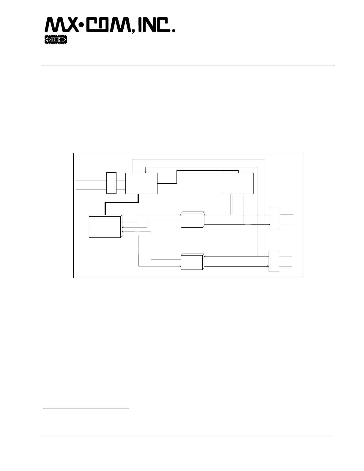
S/T Interface
CMX208
Parallel BUS
AM79C30
S/T BUS
Controller
+ Codec
1
IOM2 BUS
CLI
DTMF Rx
CMX605
•
Feature Phones
•
Pay-Phones
•
PABX Telephones
Reference Designs Available
•
Motorola
MC145480
PCM Codec
A
S
L
I
C
B
POTS 2
A
DTMF Rx
CMX605
CLI
S
L
POTS 1
I
C
B
The CMX208 is an ISDN telephony protocol engine which implements the lower level ISDN interface and
communicates with the CMX605 and other standard devices to form a fully integrated ISDN chipset for voice
communications. The CMX208 puts all the main data processing elements in a single device. No ISDN
software has to be written and simple ‘Plug and Play’ design results. This reduces development time and
provides a highly cost-effective hardware solution. By using proven circuit designs, the designer can move
quickly from initial concept through design in to manufacture.
The CMX208 supports two voice ports over the ISDN Line, which can be used to provide ISDN telephony
services or POTS line interfaces, and has independent keypad-configuration of these services for each port.
The CMX208’s feature set and architecture allow most analog systems to be converted to an ISDN equivalent
with enhanced features.
The CMX208 is designed to work with the AMD 79C30 S/T bus interface, the Siemens PSB-21525 HDLC
formatter, the Motorola MC145480 PCM codec and the MX-COM CMX605 POTS interface circuit, and also
comes complete with embedded applications software. To support the CMX208, MX-COM can also provide
licensed reference designs on user request. A flexible Applications Program Interface (API) allows users to
customize the features and operation of their own design. The CMX208 is available in an 80-pin QFP
(CMX208S1) package.
1
The CMX208 is a data processor integrated circuit that supports the protocol layers 1, 2 and 3 of the ISDN protocol stack in accordance
with the specifications of CCITT (now ITU). These specifications, which are widely used around the world, might not be supported withi n
the U.S.
MX-COM, Inc 2000 MX-COM, Inc.
4800 Bethania Station Road, Winston-Salem, NC, 27105-1201, USA Doc. # 20480214.001
www.mxcom.com tel: 800 638 5577 336 744 5050 fax: 336 744 5054 2000 Chiron Technology Limited
All trademarks and service marks are held by their respective companies

ISDN Dual Telephony Protocol Engine 2 CMX208 Advance Information
CONTENTS
Section Page
1. Block Diagram................................................................................................................3
2. Signal List.......................................................................................................................4
3. External Components....................................................................................................7
4. General Description.......................................................................................................8
4.1 Glossary............................................................................................................................... 9
4.2 Initialization ........................................................................................................................ 10
4.3 ISDN Interface.................................................................................................................... 10
4.3.1 Activation..............................................................................................................................10
4.3.2 De-activation or Line Disconnection.....................................................................................10
4.3.3 Line Failure Detection ..........................................................................................................10
4.3.4 Incoming Calls......................................................................................................................10
4.3.5 Multiple Subscriber Numbering............................................................................................11
4.3.6 Channel Mapping.................................................................................................................11
4.4 POTS Configuration........................................................................................................... 12
4.4.1 Configuration and Control via DTMF Keypad.......................................................................12
4.5 POTS Operation................................................................................................................. 13
4.5.1 Keypad Operation ................................................................................................................13
4.5.2 Incoming POTS Calls...........................................................................................................13
4.5.3 Outgoing POTS Calls...........................................................................................................13
4.5.4 Connected Calls...................................................................................................................14
4.5.5 Call Clearing.........................................................................................................................14
4.6 Application Programmer's Interface................................................................................... 14
4.7 Hardware Description......................................................................................................... 15
4.7.1 LED Status Indicators (LED1 to LED9, and ILFI).................................................................15
5. Application Notes ........................................................................................................16
5.1 General .............................................................................................................................. 16
5.2 Approvals........................................................................................................................... 16
6. Performance Specification..........................................................................................17
6.1 Electrical Performance....................................................................................................... 17
6.1.1 Absolute Maximum Ratings..................................................................................................17
6.1.2 Operating Limits...................................................................................................................17
6.1.3 Operating Characteristics.....................................................................................................18
6.2 Packaging .......................................................................................................................... 22
MX-COM, Inc. reserves the right to change specifications at any time and without notice.
MX-COM, Inc 2000 MX-COM, Inc.
4800 Bethania Station Road, Winston-Salem, NC, 27105-1201, USA Doc. # 20480214.001
www.mxcom.com tel: 800 638 5577 336 744 5050 fax: 336 744 5054 2000 Chiron Technology Limited
All trademarks and service marks are held by their respective companies
ISDN Dual Telephony Protocol Engine 3 CMX208 Advance Information
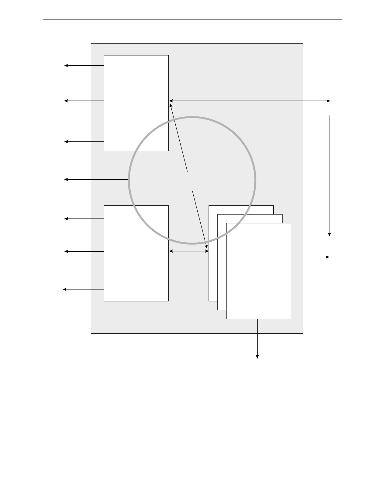
1. Block Diagram
SLIC
POTS Port 2
CMX605
DTMF Detector
and
Caller Display
LED Status
Indicators
System Memory
and NVRAM
Handler
Auxiliary
CODEC
Task Scheduler,
Memory Manager,
Timers and Task Mailing
SLIC
CMX605
DTMF Detector
and
Caller Display
LED Status
Indicators
POTS Port 1
Handler
Figure 1: Block Diagram
D-channel
Protocol
Stacks
LED Status
Indicator
ISDN
ISDN
Interface
Chip
MX-COM, Inc 2000 MX-COM, Inc.
4800 Bethania Station Road, Winston-Salem, NC, 27105-1201, USA Doc. # 20480214.001
www.mxcom.com tel: 800 638 5577 336 744 5050 fax: 336 744 5054 2000 Chiron Technology Limited
All trademarks and service marks are held by their respective companies

ISDN Dual Telephony Protocol Engine 4 CMX208 Advance Information
2. Signal List
S1 Package Signal
Pin No. Name Type
1 SCL output EEPROM - Serial Clock
2 SDA bi-directional EEPROM - Serial Data
3 ISDNRST output ISDN S-interface Chip Reset
4 N/C output Do not make any connection to this pin
5 N/C output Do not make any connection to this pin
6 N/C output Do not make any connection to this pin
7
8
RST
DV
DD1
input CMX208 Chip Reset (active low)
power
The digital positive supply rail. Levels and voltages are
dependent upon this supply. This pin should be decoupled to
DV
by a capacitor
SS
9
XTAL
output The output of the on-chip Xtal oscillator inverter
10 XTAL input The input to the oscillator inverter from the Xtal circuit
DV
11
SS1
power The digital negative supply rail (ground)
12 LED1 output POTS Port 1 Off-Hook Indicator (HK1)
13 LED2 output POTS Port 2 Off-Hook Indicator (HK2)
14 N/C output Do not make any connection to this pin
15 LED4 output POTS Port 2 Call Connected Indicator (CN2)
16 N/C output Do not make any connection to this pin
17 N/C output Do not make any connection to this pin
18 N/C output Do not make any connection to this pin
19 LED8 output ISDN Line Activated Indicator (AR)
20
ST
output Watchdog Timer Stimulus
21 LED9 output POTS Port 1 Call Connected Indicator (CN1)
22
23
WR
RD
output Memory Write Access Strobe
output Memory Read Access Strobe
24 A19 output Memory and Peripheral Address Bus
25 A18 output Memory and Peripheral Address Bus
26 A17 output Memory and Peripheral Address Bus
27 A16 output Memory and Peripheral Address Bus
28 A15 output Memory and Peripheral Address Bus
29 A14 output Memory and Peripheral Address Bus
30 A13 output Memory and Peripheral Address Bus
31 A12 output Memory and Peripheral Address Bus
32 A11 output Memory and Peripheral Address Bus
33 A10 output Memory and Peripheral Address Bus
34 A9 output Memory and Peripheral Address Bus
35 A8 output Memory and Peripheral Address Bus
36 A/D7 bi-directional Memory and Peripheral Address and Data Bus
37 A/D6 bi-directional Memory and Peripheral Address and Data Bus
38 A/D5 bi-directional Memory and Peripheral Address and Data Bus
Description
MX-COM, Inc 2000 MX-COM, Inc.
4800 Bethania Station Road, Winston-Salem, NC, 27105-1201, USA Doc. # 20480214.001
www.mxcom.com tel: 800 638 5577 336 744 5050 fax: 336 744 5054 2000 Chiron Technology Limited
All trademarks and service marks are held by their respective companies

ISDN Dual Telephony Protocol Engine 5 CMX208 Advance Information
S1 Package Signal
Description
Pin No. Name Type
39 A/D4 bi-directional Memory and Peripheral Address and Data Bus
40 A/D3 bi-directional Memory and Peripheral Address and Data Bus
41 A/D2 bi-directional Memory and Peripheral Address and Data Bus
42 A/D1 bi-directional Memory and Peripheral Address and Data Bus
43 A/D0 bi-directional Memory and Peripheral Address and Data Bus
44 ASTB output Address/Data Bus Strobe (data bus selected if low)
DV
45
46 ~ input
SS0
power The digital negative supply rail (ground)
For manufacturer's use only. Connect to DV
directly
SS
47 PSBRES output HDLC Chip Reset
48 RING2 output POTS Port 2 Ringing Generator (low when not ringing)
49
2RING
output POTS Port 2 Ringing Generator (high when not ringing)
50 API-RXD input API/RS232 Port Rx Data (inactive = high)
51 API-TXD output API/RS232 Port Tx Data (high when inactive)
52 CLIP2 output
POTS Port 2 Line Voltage Adjustment (low when sending FSK
to a Caller Display unit. If low, it makes the SLIC present a
high impedance to the POTS line)
53
B2B1/
output B-channel Select (high selects channel B1).
54 ILFI output ISDN Line Failure Indicator
DV
55
DD0
power
The digital positive supply rail. Levels and voltages are
dependent upon this supply. This pin should be decoupled to
DV
by a capacitor
SS
56 RING1 output POTS Port 1 Ringing Generator (low when not ringing)
57
1RING
58 CLIP1 output
output POTS Port 1 Ringing Generator (high when not ringing)
POTS Port 1 Line Voltage Adjustment (low when sending FSK
to a Caller Display unit. If low, it makes the SLIC present a
high impedance to the POTS line)
59 ILINE1 input
POTS Port 1 Hook Switch Status Detector
(on-hook = low)
60 ILINE2 input
POTS Port 2 Hook Switch Status Detector
(on-hook = low)
61 REPLY input CMX605 C-BUS Interface - Reply Data
62
CMD-
output CMX605 C-BUS Interface - Command Data
DATA
63 SER-CLK output CMX605 C-BUS Interface - Serial Clock
AV
64
DD
power
The positive analog supply rail. Levels and voltages are
dependent upon this supply. This pin should be decoupled to
AV
by a capacitor
SS
65
66
67
68
69
70
AV
AV
AV
AV
REF1
SS
1CS
2CS
REF2
REF3
power
power The negative analog supply rail (ground)
output CMX605 C-BUS Interface (chip select POTS Port 1)
output CMX605 C-BUS Interface (chip select POTS Port 2)
power
power
A/D Reference Voltage. Connect to AVDD directly
D/A Reference Voltage. Connect to AVDD directly
D/A Reference Voltage. Connect to AVSS directly
MX-COM, Inc 2000 MX-COM, Inc.
4800 Bethania Station Road, Winston-Salem, NC, 27105-1201, USA Doc. # 20480214.001
www.mxcom.com tel: 800 638 5577 336 744 5050 fax: 336 744 5054 2000 Chiron Technology Limited
All trademarks and service marks are held by their respective companies

ISDN Dual Telephony Protocol Engine 6 CMX208 Advance Information
S1 Package Signal
Description
Pin No. Name Type
71 NMI input
For manufacturer's use only. Connect to DV
directly
SS
72 API-INT input API Interrupt (inactive = high)
73
IRQ
input CMX605 C-BUS Interface - Interrupt (inactive = high)
74 PSBINT input HDLC Chip Interrupt
75
76
∼
∼
input
input
For manufacturer’s use only. Connect to DV
For manufacturer’s use only. Connect to DV
DD
DD
directly
directly
77 ISDNINT input ISDN S-interface Chip Interrupt
78
79
∼
∼
input
For manufacturer’s use only. Connect to DV
For manufacturer’s use only. Connect to DV
DD
DD
directly
directly
80 N/C output Do not make any connection to this pin
Table 1: Signal List
MX-COM, Inc 2000 MX-COM, Inc.
4800 Bethania Station Road, Winston-Salem, NC, 27105-1201, USA Doc. # 20480214.001
www.mxcom.com tel: 800 638 5577 336 744 5050 fax: 336 744 5054 2000 Chiron Technology Limited
All trademarks and service marks are held by their respective companies
ISDN Dual Telephony Protocol Engine 7 CMX208 Advance Information
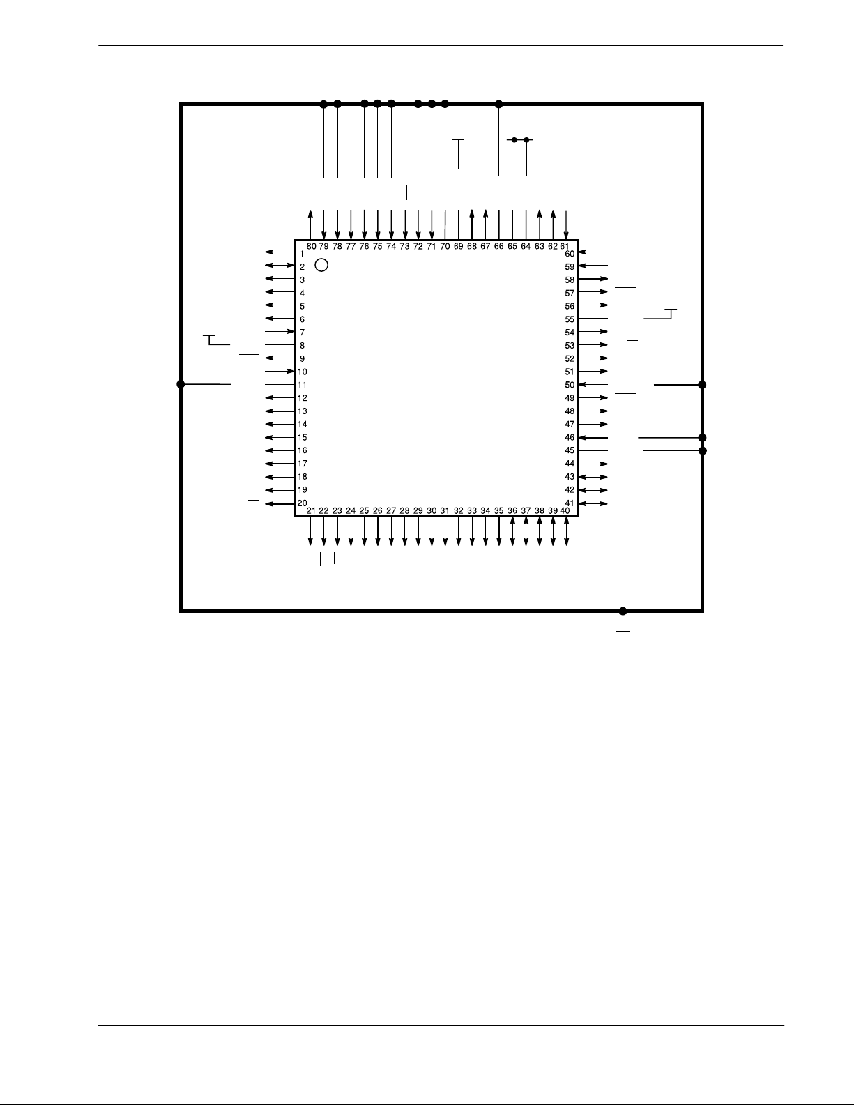
3. External Components
V
DD
SCL
SDA
ISDNRST
N/C
N/C
N/C
RST
DV
DD1
XTAL
XTAL
DV
SS1
LED1
LED2
N/C
LED4
N/C
N/C
N/C
LED8
CS2
CS1
V
DD
SS
REF1
DD
AV
AV
AV
REPLY
SER-CLK
CMD-DATA
ILINE2
ILINE1
CLIP1
RING1
RING1
DV
ILFI
B1/B2
CLIP2
API-TXD
API-RXD
RING2
RING2
N/C
(V )
DV
ASTB
A/D0
A/D1
A/D2
SS
DD0
SS0
V
DD
V
DD
REF2
N/C
SS
SS
SS
(V )
(V )
(V )
ISDNINT
SS
SS
(V )
(V )
IRQ
API-INT
NMI
REF3
AV
AV
CMX208S1
ST
LED9
WR
RD
A19
A18
A17
A16
A15
A14
A13
A12
A11
A10
A9
A/D7
A/D6
A/D5
A/D4
A/D3
V
SS
A8
Figure 2: CMX208 Pin-Out
This product is to be used as part of a chip-set. Please refer to the Applications Section (Section 5) for
Note:
details of the recommended chip-set.
MX-COM, Inc 2000 MX-COM, Inc.
4800 Bethania Station Road, Winston-Salem, NC, 27105-1201, USA Doc. # 20480214.001
www.mxcom.com tel: 800 638 5577 336 744 5050 fax: 336 744 5054 2000 Chiron Technology Limited
All trademarks and service marks are held by their respective companies
 Loading...