

DATA BULLETIN
CMX017
UHF FM/FSK Transmitter
ADVANCE INFORMATION
Features Applications
•
Direct FM/FSK UHF Modulator
•
Adjustable Modulator Output Power
•
Integrated Power Amplifier with Output
Power up to +20dBm (100mW)
•
Low Power 2.7V Operation
•
Powersave and Zero-Power
(<10µA) Modes
•
28-Pin SSOP Package
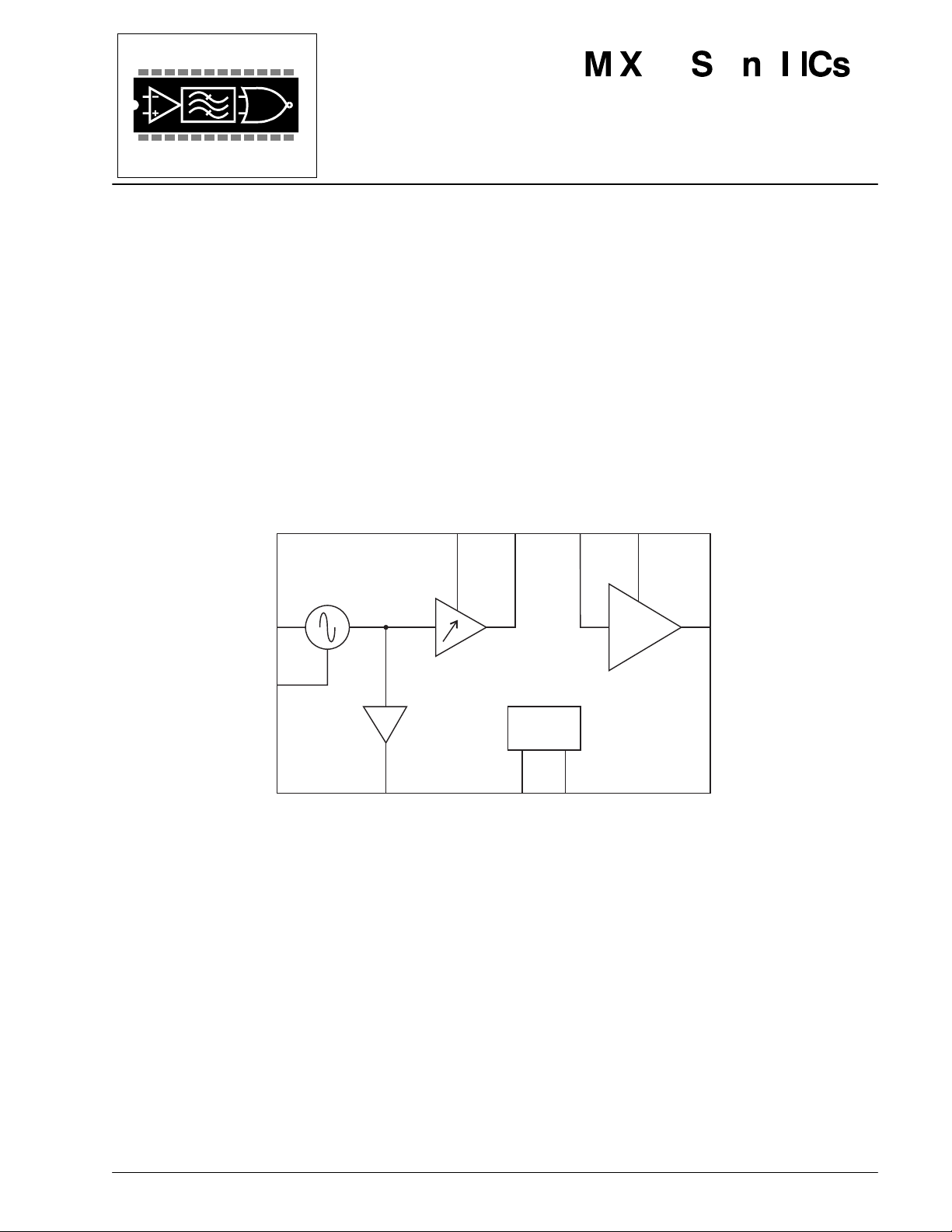
MODIN
FM/FSK
MODULATOR
POWER
AMPLIFIER
DRIVER
GAIN MODOUT PAIN IPAOUT
•
General Radio Link 860-965MHz
•
General 915MHz ISM Band (USA)
•
Spread Spectrum Wireless
Systems
•
Fixed Frequency Transmissions
•
Analog/Digital Cordless Phones
•
Handheld Data Terminals
•
SO-HO Wireless Data Links
POWER
AMPLIFIER
PAOUT
TAN K
BUFFERED
OSCILLATOR
OUTPUT
OSCOUT
The CMX017 is a single chip UHF FM/FSK transmitter that combines both the RF VCO Modulator and RF
Power Amplifier. It is suitable for both audio FM and digital FSK transmissions.
A buffered oscillator output provides the RF signal drive to an external synthesizer or fixed frequency phaselocked loop for channel frequency selection. Modulator output power is adjustable over a 20dB range and the
integrated power amplifier delivers up to +20dBm. The device also includes a powersave mode: “Transmit
Standby” and a zero-power mode: “Sleep”. These allow independent power down control of both the
modulator and power amplifier, thereby maximizing battery life. The device can be used in conjunction with
the CMX018, a double-conversion super-heterodyne receiver, to implement a complete UHF radio link.
The CMX017 operates from a 2.7V to 3.3V power supply and is available in the following package style:
28-pin SSOP (CMX017D6).
BANDGAP & BIAS
CONTROL
ENLMOD
ENLPA
1999 MX-COM, Inc. www.mxcom.com Tel: 800 638 5577 336 744 5050 Fax: 336 744 5054 Doc. # 20480193.003
4800 Bethania Station Road, Winston-Salem, NC 27105-1201 USA All trademarks and service marks are held by their respective companies

UHF FM/FSK Transmitter 2 CMX017 Advance Information
CONTENTS
Section Page
1 Block Diagram................................................................................................................3
2 Signal List.......................................................................................................................4
3 External Components....................................................................................................5
4 General Description.......................................................................................................6
4.1 FM/FSK Modulator + PA Driver........................................................................................... 6
4.2 Power Amplifier (PA) ........................................................................................................... 6
4.3 Power-Down Modes ............................................................................................................ 6
5 Application Notes ..........................................................................................................6
5.1 Generation of the Modulated RF Signal .............................................................................. 6
5.2 Power-Down Modes ............................................................................................................ 7
6 Performance Specification..........................................................................................10
6.1 Electrical Performance ...................................................................................................... 10
6.1.1 Absolute Maximum Ratings.................................................................................................. 10
6.1.2 Operating Limits...................................................................................................................10
6.1.3 Operating Characteristics.....................................................................................................10
6.1.4 Packaging.............................................................................................................................12
MX-COM, Inc reserves the right to change specifications at any time and without notice.
1999 MX-COM, Inc. www.mxcom.com Tel: 800 638 5577 336 744 5050 Fax: 336 744 5054 Doc. # 20480193.003
4800 Bethania Station Road, Winston-Salem, NC 27105-1201 USA All trademarks and service marks are held by their respective companies
UHF FM/FSK Transmitter 3 CMX017 Advance Information
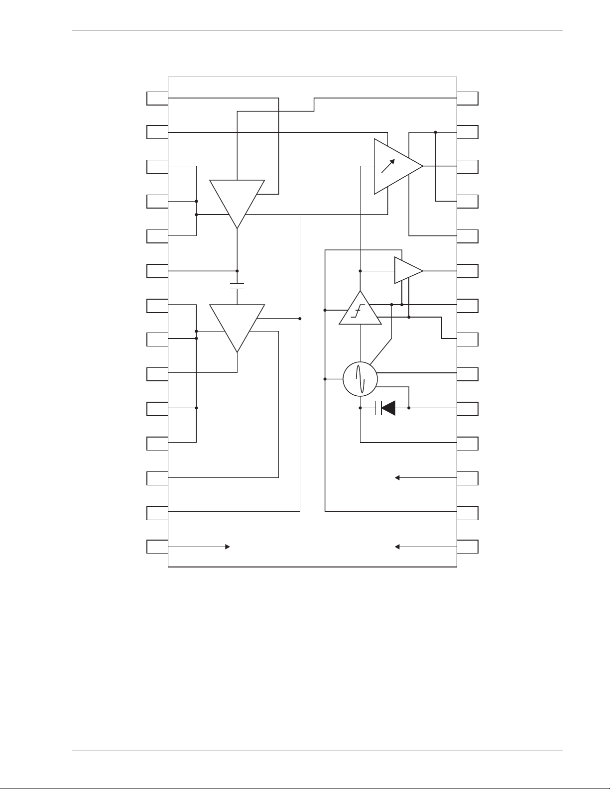
1 Block Diagram
V3
CC
GAIN
GND
GND
GND
IPAOUT
GND
GND
PAOUT
1
2
P A DRIVER
3
PA
4
ST AGE 1
5
BUFFERED
OSCILLATOR
OUTPUT
6
7
PA
ST AGE 2
8
FM/FSK
MODULATOR
9
28
27
26
25
24
23
22
21
20
PAIN
GND
MODOUT
GND
V2
CC
OSCOUT
V1
CC
GND
TANK
10
GND
11
GND
V4
ENLPA
12
CC
13
PACKAGE
14
GND GND
GROUND
SUBSTRA TE
PACKAGE
GROUND
19
18
17
16
15
Figure 1: Internal Block Diagram
GND
MODIN
GND
ENLMOD
1999 MX-COM, Inc. www.mxcom.com Tel: 800 638 5577 336 744 5050 Fax: 336 744 5054 Doc. # 20480193.003
4800 Bethania Station Road, Winston-Salem, NC 27105-1201 USA All trademarks and service marks are held by their respective companies

UHF FM/FSK Transmitter 4 CMX017 Advance Information
2 Signal List
Pin No. Signal
Description
D6 Package Name Type
1V
3 power Power amplifier (first stage) power supply - nominally 3.0V
CC
2 GAIN input Modulator output (pin 26) - Power control
3 GND ground Ground-plane connection to the power amplifier
4 GND ground Ground-plane connection to the power amplifier
5 GND ground Ground-plane connection to the power amplifier
6 IPAOUT output Output (open-collector) from the first stage of the power
amplifier
7 GND ground Ground-plane connection to the power amplifier
8 GND ground Ground-plane connection to the power amplifier
9 PAOUT output
Output (open-collector) from the second stage of the power
amplifier
10 GND ground Ground-plane connection to the power amplifier
11 GND ground Ground-plane connection to the power amplifier
12 VCC4 power Power amplifier (second stage) power supply
– nominally 3.0V
13 ENLPA
CMOS
input
Power Amplifier powersave logic control. A logic “0” powers
down the Power Amplifier and Driver stages
14 GND ground Ground-plane connection
15 GND ground Ground-plane connection
16 ENLMOD CMOS
input
Modulator zero-power logic control. A logic “0” powers down
the Modulator and Buffered Oscillator stages
17 GND ground Ground-plane connection
18 MODIN input Baseband modulation input signal
19 GND ground Ground-plane connection to the VCO
20 TANK input VCO Tank circuit/Resonator connection
21 GND ground Ground-plane connection to the modulator and VCO buffer
22 VCC1 power Modulator power supply – nominally 3.0V
23 OSCOUT output Buffered Oscillator (open-collector) output
24 VCC2 power Power Amplifier Driver power supply - nominally 3.0V
25 GND ground Ground-plane connection for the Power Amplifier Driver
26 MODOUT output Modulator output
27 GND ground Ground-plane connection for the Power Amplifier Driver
28 PAIN input Power Amplifier input
Table 1: Signal List
1999 MX-COM, Inc. www.mxcom.com Tel: 800 638 5577 336 744 5050 Fax: 336 744 5054 Doc. # 20480193.003
4800 Bethania Station Road, Winston-Salem, NC 27105-1201 USA All trademarks and service marks are held by their respective companies
 Loading...