

MUSIC MUSA16P14-B456C Datasheet

Preliminary Data Sheet
MUSIC Semiconductors, the MUSIC logo, and the phrase "MUSIC Semiconductors" are
October 10, 2000 Rev. 2.7 Draft
Registered trademarks of MUSIC Semiconductors. MUSIC and Epoch are trademarks of
MUSIC Semiconductors.
APPLICATIONS
• WAN edge routers
• MultiService platforms
•RAS platforms
• Group Switch/Rout er
•DSLAMs
• LAN PBX core
FEATURES AND BENEFITS
• MultiMedia-ready integrated switch on a chip
• Process Layer 3 and Layer 4 of the IP stack
• 1.4 Million packets/flow classifications per second; full Layer 4 flow recognition
• Up to 16 ports supported with powerful flexible built-in parsing functio n
• QoS Support for VoIP and other MultiMedia flows
• Differentiated Services per port (DS)
• Eight queues per output port enabling efficient MultiMedia integration of voice (VoIP), video, and data
• Two scheduling algorithms selecta ble on a per port basis.
• IPv6 and other protocols supported through processor interface
• No Head-of-line blocking
• Layer 2 switch-through support at wire speed
• Firewall assist on a per packet or per flow basis
• Flow aging support
DISTINCTIVE CHARACTERISTICS
• Wire speed Layer 3/Layer 4 switching for IPv4, IP Multicast, and IPX
• Header manipulation and checksum recalculation at wire speeds
• Support for Layer 3 CIDR (best prefix match)
• Per Flow and per IP or IPX address filtering option s
• Behavior Aggregate Classification (BAC) and Microflow static/dynamic flow classification
• 64K default priority assignments with processor override for specific flows
• Eight levels of Weighted RR or eight levels of priority
• L3 to L2 support for IP to MAC address translation
• Destination and/or Source Port monitoring
• Generic 32 bit processor interface
• 66 MHz clock
• 3.3 Volt power with 5 Volt tolerant I/O pins
• IEEE 1149.1 (JTAG) boundary scan logic
• 456 PBGA Package
Related MUSIC Documentation:
Epoch Host Processor Software Development Manual
MUAC Routing CoProcessor (RCP) Family Data Sheet
AN-N25 Fast IPv4 and IPv4 CIDR Address Translation and Filtering Using the MUAC Routing CoProces sor (RCP)
Application Note
AN-N27 Using MUSIC Devices and RCPs for IP Flow Recognition Application Note
Epoch MultiLayer Switch Chipset
Epoch MultiLayer Switch ChipsetEpoch MultiLayer Switch Chipset
Epoch MultiLayer Switch Chipset
Epoch MultiLayer Switch Chipset Operational Overview
2
Rev . 2.7 Draft
OPERATIONAL OVERVIEW
The MUSIC Epoch MultiLayer Switch Chip for a Layer
3/4 switch performs all of the functions necessary to route
IPv4, IPX and IP Multicast packets at wire-speed; to
recognize and categorize traffic flows, optionally using
IETF Differentiated Services (DS); and to queue each flow
independently in an associated SDRAM. Upon
transmission, DS information may be remarked. The
Epoch handles up to 16 ports; one port is required for the
processor to allow it to act as a packet source or
destination.
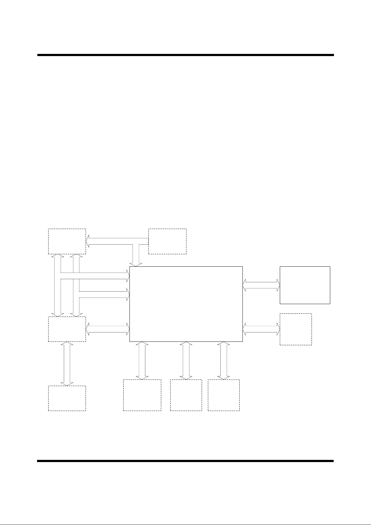
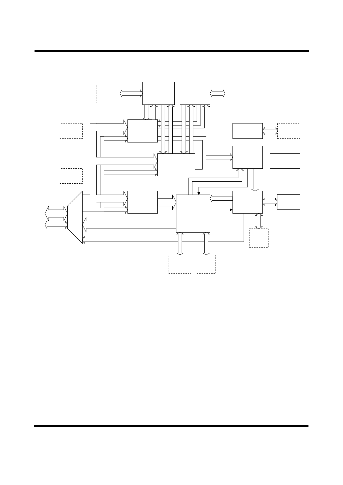
The Epoch chip fits into a system as shown in Figure 1.
The Epoch chip itself is the heart of the system and forms
the basis of a Layer 3/4 switch with up to 16 ports, one of
which is used for the processor to send and receive
packets. Each port has eight queues and a queue scheduler
determines queue service order for each output por t. Layer
3 and Layer 4 information are stored in a Routing
CoProcessor (RCP) database. The RCP provides the
packet header processing per forma nce necess ary to do true
wire-speed packet-by-packet routing and real-time flow
recognition. The Epoch has a multicast switch fabric that
also can be used for Layer 2 switches and xDSL
multiplexers.
Various SRAM and SDRAM devices are required to store
packet data and internal Epoch control information.
A processor provides non-real-time initialization and
housekeeping functions. A pr ocessor also is used t o handle
packets destined to the switch and packets not supported
by the Epoch. One processor may be used to handle both
of these functions or separate processors may be used.
The Arbiter controls access to the bidirectional data bus
among the Layer 2 ports, including the processor interface
to the data bus. These components are detailed later.
Figure 1: EPOCH MultiLayer Switch in a System
MUSIC Semiconductors
EPOCH MultiLayer Switch
MUSIC
Semiconductors
MUAC Routing
CoProcessor
4K-32K x 64
MUAC Bus
Arbiter
Processor or
Processors
SDRAM Bus
Arbiter Bus
Data Bus
Control Bus
Processor
Interface
Processor Bus
Processor Bus
Layer 2
Interface(s)
SDRAM Bus
Packet Data
SDRAM
1M x 16 (2x)
Packet
Control
SDRAM
1M x 16
SRAM Bus
Packet
Pointer
SRAM
64K x 32
SRAM Bus
L3/L4
Database
SRAM
128K x 16
Note:
Solid boxes denote MUSIC standard products; dashed boxes denote either standard products; dashed boxes denote standard products from other
manufacturers or customer ASICs/FPGAs/PLDs.
Ball Descriptions Epoch MultiLayer Switch Chipset
Rev. 2.7 Draft
3
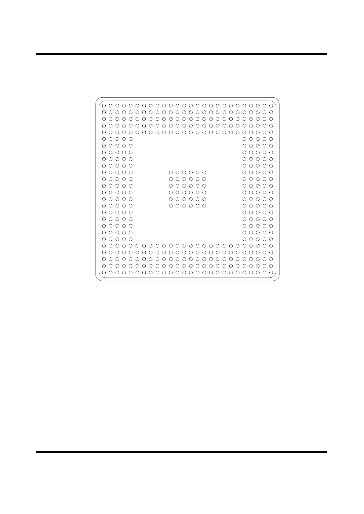
BALL DESCRIPTIONS
This section contains ball descriptions. Refer to Figure 2 below and Table 1, Ball Descriptions, on page 4.
Figure 2: PBGA Ball Diagram (Underside View)
AF
AE
AD
AC
AB
AA
Y
W
V
U
T
R
P
N
M
L
K
J
H
G
F
E
D
C
B
A
2625242322212019181716151413121110987654321
Epoch MultiLayer Switch Chipset Ball Descriptions
4
Rev . 2.7 Draft
Table 1: Ball Descriptions
Functional
Group
Ball Name(s)
(Appended b
indicates
active low signal)
Function Type PBGA Ball(s)
I/O TDM Bus L2DATA[31:0]
Interface to Layer 2
Devices.
TDM Data Bus.
Transmit and receive data bursts in 64 byte blocks.
Bidir
TTL
5V Tol.
b0:D14, b1:A13, b2:B13,
b3:C13, b4:D13, b5:B12,
b6:C12, b7:D12, b8:A11,
b9:B11, b10:C11, b11:D11,
b12:A10, b13:B10, b14:C10,
b15:D10, b16:A9, b17:B9,
b18:C9, b19:D9, b20:A8,
b21:B8, b22:C8, b23:D8,
b24:A7, b25:B7, b26:C7,
b27:D7, b28:A6, b29:B6,
b30:C6, b31:D6
L2CNTL[7:0] TDM Control Bus.
Transmit and receive control information.
Bidir
TTL
5V Tol.
b0:D16, b1:A15, b2:B15,
b3:C15, b4:D15, b5:A14,
b6:B14, b7:C14
SYNC TDM Timeslot. Synchronization Signal. Position is
programmable.
Output
TTL
B17
ABORT Aborts the current receive packet indication. Assert
for one CLK. May be asserted from the first word of a
receive packet data bur st, CLK 4 to CLK 47 of a bus
cycle. Overrides or replaces LASTWORD and
LASTBYTE[1:0].
Input
TTL
D19
L2RXREADYIN Asserted by L2 device when it has data next slot.
Sampled by Epoch in CLK4.
Input
TTL
5V Tol.
B16
L2TXREAD Y IN Asserted by L2 device when it can accept data next
slot.
Sampled by Epoch in CLK4.
Input
TTL
5V Tol.
A16
L2TXREAD YOUT Asserted to L2 device indicating data is availab le this
slot. Asserted by Epoch in CLK11, de-asserted
CLK30.
Output
TTL
C16
L2LASTWORD Asserted for one CLK at the CLK of the last word of a
packet in the last buffer of a packe t for both TX and
RX packets.
Bidir
TTL
5V Tol.
A17
L2LASTBYTE[1:0] Indicates the last byte of the last word of a packet for
both TX and RX packets. Encoding is as follows:
Bidir
TTL
5V Tol.
b0:C17, b1:D17
Arbiter Bus L2NEXTPORT[3:0] Inputs number of next active port.
Sampled a TDM cycle ahead in CLK2.
Input
TTL
5V Tol.
b0:A18, b1:B18, b2:C18,
b3:D18
31 L2DATA 0
Byte 0 Byte 1 Byte 2 Byte 3 L2LASTBYTE[1:0]
Valid Invalid Invalid Invalid 00
Valid Valid Invalid Invalid 01
Valid Valid Valid Invalid 10
Valid Valid Valid Valid 11

Ball Descriptions Epoch MultiLayer Switch Chipset
Rev. 2.7 Draft
5
BFM Data
SDRAM.
Buffer Manager
interface to data
buffer RAM.
BSDRAMD[31:0] Buffer Data SDRAM
Data Bus
Bidir
TTL
3.3V
Only
b0:F24, b1:F23, b2:E26,
b3:E25, b4:E24, b5:E23,
b6:D26, b7:D25, b8:D24,
b9:C26, b10:C25, b11:A25
b12:A24, b13:B24, b14:A23,
b15:B23, b16:C23, b17:A22,
b18:B22, b19:C22, b20:D22,
b21:A21, b22:B21, b23:C21,
b24:D21, b25:A20, b26:B20,
b27:C20, b28:D20, b29:A19,
b30:B19, b31:C19
BSDRAMA[10:0] Buffer Data SDRAM
Address Bus
Output
TTL
b0:J23, b1:H26, b2:H25,
b3:H24, b4:H23, b5:G26,
b6:G25, b7:G24, b8:G23,
b9:F26, b10:F25
BSDRAMBS Buffer Data SDRAM
Bank Select
Output
TTL
J24
BSDRAMRASb Buffer Data SDRAM
Row Address Strobe
Output
TTL
J26
BSDRAMCASb Buffer Data SDRAM
Column Address Strobe
Output
TTL
J25
BSDRAMWEb Buffer Data SDRAM
Write Enable Strobe
Output
TTL
K23
BSDRAMDQM Buffer Data SDRAM
Data Mask
Output
TTL
K24
BFM Po inter
SDRAM.
Buffer Manager
interface to
pointer RAM.
PSDRAMD[15:0] Control SDRAM
Data Bus
Bidir
TTL
3.3V
Only
b0:P24, b1:P23, b2:N26,
b3:N25, b4:N24, b5:N23,
b6:M26, b7:M25, b8:M24,
b9:M23, b10:L26, b11:L25,
b12:L24, b13:L23, b14:K26,
b15:K25
PSDRAMA[10:0] Control SDRAM
Address Bus
Output
TTL
b0:U23, b1:T26, b2:T25,
b3:T24, b4:T23, b5:R26,
b6:R25, b7:R24, b8:R23,
b9:P26, b10:P25
PSDRAMBS Control SDRAM
Bank Select
Output
TTL
U26
PSDRAMRASb C ontrol SDRAM
Row Address Strobe
Output
TTL
U24
PSDRAMCASb C ontrol SDRAM
Column Address Strobe
Output
TTL
U25
PSDRAMWEb Control SDRAM
Write Enable Strobe
Output
TTL
V24
PSDRAMDQM
ica
Control SDRAM
Data Mask
Output
TTL
V23
Table 1: Ball Descriptions (continued)
Functional
Group
Ball Name(s)
(Appended b
indicates
active low signal)
Function Type PBGA Ball(s)

Epoch MultiLayer Switch Chipset Ball Descriptions
6
Rev . 2.7 Draft
PKM SRAM.
Packet manager
SRAM interface.
PKTSRAMDATA
[31:0]
Packet SRAM
Data Bus
Bidir
TTL
3.3V
Only
b0:AE22, b1:AD22, b2:AC22,
b3:AF23, b4:AE23, b5:AD23,
b6:AF24, b7:AE24, b8:AE26,
b9:AD26, b10:AD25, b11: AC26,
b12:AC25, b13:AC24, b14:AB26,
b15:AB25, b16:AB24, b17:AB23,
b18:AA26, b19:AA25, b20:AA24,
b21:AA23, b22:Y26, b23:Y25,
b24:Y24, b25:Y23, b26:W26,
b27:W25, b28:W24, b29:W23,
b30:V26, b31:V25
PKTSRAMAD-
DRESS [15:0]
Packet SRAM
Address Bus
Output
TTL
b0:AE18, b1:AD18, b2:AC18,
b3:AF19, b4:AE19, b5:AD19,
b6:AC19, b7:AF20, b8:AE20,
b9:AD20, b10:AC20, b11:AF21,
b12:AE21, b13:AD21, b14:AC21,
b15:AF22
PKTSRAMWEb Packet SRAM
Write Enable
Output
TTL
AF18
PKTSRAMOEb Packet SRAM Output
TTL Enable
Output
TTL
AF17
CRI RCP.
Glue free Con-
nection to the
MUSIC MUAC
RCP.
RCPAC[12:0] RCP Address Control Inputs Bidir
TTL
3.3V
Only
b0:AC13, b1:AF14, b2:AE14,
b3:AD14, b4:AC14, b5:AF15,
b6:AE15, b7:AD15, b8:AC15,
b9:AF16, b10:AE16,b11:AD16,
b12:AC16
RCPFFb RCP Full Flag Input
TTL
3.3V
Only
AC17
RCPMFb RCP Match Flag Input
TTL
3.3V
Only
AE17
RCPMMb RCP Multimatch Flag Input
TTL
3.3V
Only
AD17
RCPAVb
Dual use pin, see
PLL section.
RCP Address Valid PLL ENABLE
Pull HIGH through 4K7R if CLK = 50-66MHz
Pull LOW through 4K7R if CLK = 0-50MHz
Bidir
TTL
3.3V
Only
AD5
RCPCS20b Chip select2 for first RCP Output
TTL
AF5
RCPCS21b Chip select2 for second RCP Output
TTL
AE5
RCPCS22b Chip select2 for third RCP Output
TTL
AF4
RCPCS23b Chip select2 for fourth RCP Output
TTL
AE4
Table 1: Ball Descriptions (continued)
Functional
Group
Ball Name(s)
(Appended b
indicates
active low signal)
Function Type PBGA Ball(s)

Ball Descriptions Epoch MultiLayer Switch Chipset
Rev. 2.7 Draft
7
CRI RCP.
Glue free Con-
nection to the
MUSIC MUAC
RCP.
(continued)
RCPDSC Data Segment Control
Output
Output
TTL
AF3
RCPDQ[31:0] RCP Data Bus Bidir
TTL
3.3V
Only
b0:AC5, b1:AF 6, b2:AE6, b3:AD6,
b4:AC6, b5:AF 7, b6:AE7, b7:AD7,
b8:AC7, b9:AF 8, b10:AE8,
b11:AD8, b12:AC8, b13:AF9,
b14:AE9, b15:AD9, b16:AC9,
b17:AF10, b18:AE10, b19:AD10,
b20:AC10, b21:AF11, b22:AE11,
b23, AD11, b24:AC11, b25:AF12,
b26:AE12, b27:AD12, b28:AC12,
b29:AF13, b30:AE13, b31:AD13
RCPEb RCP Chip Enable Output
TTL
AD1
RCPOEb RCP Output Enable Output
TTL
AD2
RCPRESETb RCP Reset Output
TTL
AD4
RCPVBb RCP Validity Bit Bidir
TTL
3.3V
Only
AE3
RCPWb RCP Write Enable Output
TTL
AF2
RCPADDR[14:0] CRI Shared RCP and Associated Data SRAM
Address Bus. Connect to AA12:0 on RCPs and to
Address pins of CRI SRAM.
Bidir
TTL
3.3V
Only
b0:W3, b1:W4, b2:Y1, b3:Y2,
b4:Y3, b5:Y4, b6:AA1, b7:AA2,
b8:AA3, b9:AA4, b10:AB1,
b11:AB2, b12:AB3, b13:AB4,
b14:AC1
Interface to the
CRI Associated
Data SRAM
SRAMADDR [16:15] CRI High SRAM Address Bits
SRAM Address [16:15]
Output
TTL
b15:AC2, b16:AC3
SRAMDQ[15:0] CRI SRAM
Data Bus
Bidir
TTL
3.3V
Only
b0:R3, b1:R4, b2:T1, b3:T2,
b4:T3, b5:T4, b6:U1, b7:U2,
b8:U3, b9:U4, b10:V1, b11:V2,
b12:V3, b13:V4, b14:W1,
b15:W2
SRAMOEb CRI SRAM
Output Enable
Output
TTL
R2
SRAMWEb CRI SRAM
Write Enable
Output
TTL
R1
Processor
Interface
PDATA[31:0] Processor Data Bus Bidir
TTL
5V Tol.
b0:C1, b1:D1, b2:D2, b3:D3,
b4:E1, b5:E2, b6:E3, b7:E4,
b8:F1, b9:F2, b10:F3, b11:F4
b12:G2, b13:G3, b14:G4,
b15:H1, b16:H2, b17:H3,
b18:H4, b19:J1, b20:J2, b21:J3,
b22:J4, b23:K1, b24:K2,
b25:K3, b26:K4, b27:L1, b28:L2,
b29:L3, b30:L4, b31:M1
Table 1: Ball Descriptions (continued)
Functional
Group
Ball Name(s)
(Appended b
indicates
active low signal)
Function Type PBGA Ball(s)

Epoch MultiLayer Switch Chipset Ball Descriptions
8
Rev . 2.7 Draft
Processor
Interface
(continued)
PRWb Processor Read/Write Input
TTL
5V Tol.
P4
PCSb P rocessor Chip Select. May be asynchronous to
CLK.
Input
TTL
5V Tol.
P2
PREADY Proce ssor Ready Active present cycle may complete Output
TTL
P3
PADDR[8:2] Processor Address Input
TTL
5V Tol.
b2:M3, b3:M4, b4:N1, b5:N2,
b6:N3, b7:N4, b8:P1
INT Interrupt to Processor Output
TTL
M2
JTAG TDI Test Data In Input
TTL
5V Tol.
B5
TCLK Test Clock Input
TTL
5V Tol.
C4
TMS Test Mode Select Input
TTL
5V Tol.
B3
TDO Test Data Out Output
TTL
C5
TRST Test Reset Input
TTL
5V Tol.
A4
PLL ZLOOP Filter Input Input A3
Miscellaneous RESETb Device Reset. Must be active for 2 CLKS min. Chip
takes 5 CLKS to come out of reset from RESETb
LOW to HIGH
Input
TTL
Schmid
t
5V Tol.
B4
CLK Device Clock Input
CMOS
TTL
5V Tol.
A5
Power 3.3V Device Power 3.3 Volts N/A AB11, AB13, AB 14, AB16,
AB18, AB20, AB7, AB9, E11,
E13, E14, E16, E18, E20, E7,
E9, G22, G5, J22, J5, L22, L5,
N22, N5, P22, P5, T22, T5, V22,
V5, Y22, Y5
Table 1: Ball Descriptions (continued)
Functional
Group
Ball Name(s)
(Appended b
indicates
active low signal)
Function Type PBGA Ball(s)
Ball Descriptions Epoch MultiLayer Switch Chipset
Rev. 2.7 Draft
9
Power
(continued)
GND Device Ground N/A A1, A2, A26, AA22, AA5, AB10,
AB12, AB15, AB17, AB19,
AB21, AB22, AB5, AB6, AB8 ,
AC23, AC4, AD24, AD3, AE1,
AE2, AE25, AF1, AF25, AF26,
B2, B25, B26, C24,C3, D23, D4,
E10, E12, E15, E17, E19, E21,
E22, E5, E6, E8, F22, F5, H22,
H5, K22, K5, M22, M5, R22, R5,
U22, U5, W22, W5, L16-11,
M16-11, N16-11, P16-11,
R16-11, T16-11
VDDWELL5V Connect to 5 Volts for 5 Volt tolerant buffers. Connect
to 3.3 Volts if no 5 Volt tolerance is required.
N/A G1, A12
AVDD Analog VDD. Quiet VDD for PLL (3.3V) N/A B1
AVSS Analog VSS. Quiet VSS for PLL. N/A D5
VDDWELLPLL PLL well 3.3V. Connect to quiet VDD. N/A C2
Table 1: Ball Descriptions (continued)
Functional
Group
Ball Name(s)
(Appended b
indicates
active low signal)
Function Type PBGA Ball(s)
Epoch MultiLayer Switch Chipset Functional Overview
10
Rev . 2.7 Draft
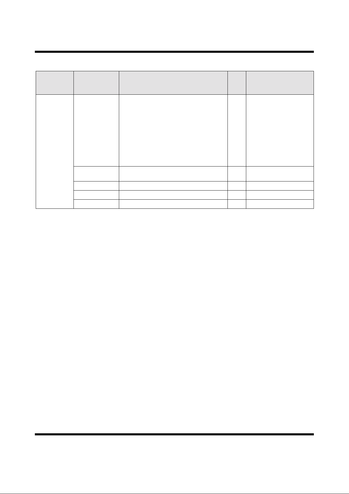
FUNCTIONAL OVERVIEW
Figure 3: Epoch MultiLayer Switch Functional Block Diagram
Block Diagram Overview
The functional block diagram above (Figure 3) splits the
Epoch chip into several blocks. Data moves to and from
the Epoch via data and control buses with synchronized
timeslots. The timeslots are long eno ugh to move 64 bytes
of data into the Epoch followed by 64 bytes of data from
the Epoch. For longer packets, multiple timeslots are
necessary. Timeslots for different Layer 2 ports interleave
on the bus. Timeslots are 48 clock cycles and the
minimum clock period is 15 ns; 16 clock cycles are for
data movement into the E poch and 16 clock cycles for data
movement from the Epoch via a 32-bi t bu s. The remai n ing
cycles are for system overhead.
There are eight queues for each of the 16 output ports. An
on-chip scheduler with two modes of operation schedules
among the queues. Queue zero has the highest priority and
queue seven has the lowest priority.
• Mode 1- Weighted Round Robin
• Mode 2- Priority Order
Modes are selectable per port.
Main Multiplexer (PIF)
The Main Multiplexer (PIF) interfaces the bidirectional
data and control buses used outside the Epoch chip to
unidirectional data and control buses used inside the chip.
The major function of the PIF is bus multiplexing. In
addition, the PIF inserts Differentiated Service
information to selected transmitted packets.
Arbiter
Processor
Packet
Data
SDRAM
1M x 16 (2x)
Data Bus
Control Bus
Data Bus
Buffer
Manager
(BFM)
Control Bus
Control Bus
Data Bus
PEN
Control Bus
SDRAM Bus
Main
Mux
(PIF)
Data Bus
MUAC
Routing
CoProcessor
4K-32K x 64
Data Bus
Control Bus
L3 PEN
L4 PEN
Multicast
Manager
(MCM)
MUAC bus
Packet
Manager
(PKM)
Control Bus
Data Bus
Control Bus
Packet
Pointer
SRAM
64K x 32
SDRAM Bus
Packet
Control
SDRAM
1M x 16
Firewall
Queue
Scheduler
(QSM)
L3/L4
Database
SRAM
128K x 16
Control Bus
Processor
Interface (PIM)
Statistics
Module (STM)
CRI RCP Interface
CRI SRAM
Interface
Control Bus

Functional Overview Epoch MultiLayer Switch Chipset
Rev. 2.7 Draft
11
Buffer Manager (BFM)
The Buffer Ma nager (BFM) i s resp onsibl e for storin g and
extracting packets from the SDRAM. All packet switching
occurs in the SDRAM. The Packet Data SDRAM stores
the packet data received by the Epoch. The Packet Control
SDRAM stores linked list information as well as data
associated with each packet. Separate SDRAMs are used
for packet data and BFM control information. If a packet
is larger than the size of a buffer, then the BFM is
responsible for chaining together buffers to hold an entire
packet.
The BFM also tracks the number of queues that point to
each packet. This number decrements after packet
transmission. When this number reaches zero, the buffers
return to the free buffer pool.
L3/L4 Database
The L3/L4 Database RCP consists of up to four cascaded
RCPs from the MUSIC MUAC Routing CoProcessor
family. These RCPs provide the ability to perform 32-bit
longest match address lookup or 64-bit exact address
lookup. The RCPs contain the IP, IPX and IP Multicast
routing tables, along with matched (see CRI section),
authenticated flow information. See MUSIC Application
Note AN-N25 for more detailed information on Layer 3
address lookup. See MUSIC Application Note AN-N27
for more detailed information on Layer 4 flow recognition.
RCP/RAM Interface (CRI)
The RCP/RAM Interface (CRI) interface contains the state
machines for driving the RCP and associated data R AM as
well as the logic to arbitrate among the sources of RCP
operations (PEN and PIM ).
Database SRAM
The external L3/L4 Database SRAM contains the
Differentiated Services data associated with each word
contained in the L3/L4 Database RCP as well as default
queuing information based on TCP/UDP port number for
unrecognized flows and the Differentiated Services BAC
mode Table.
Parse Engine (PEN)
The Parse Engine (PEN) comprises the L3 data
manipulation, L3 Lookup and L4 Look up sectio ns. The L3
Data Parse Engine makes the appropriate changes to the
header of each IP or IPX packet that passes through the
Epoch, such as decrementing the TTL field and
recomputing the header checksum on IP or the Transport
Control field on IPX. If the packet is not an IP or IPX
packet, the header is unchanged. The PEN verifies various
fields of th e IPv4 or IPX he ader.
The L3 Engine in the PEN is responsible for extracting the
IPv4, IP Multicast, or IPX address from the packet and
using the RCP (via the CRI) to determine the output
port(s) to which the packet is to be sent. The RCP returns
the index of a matching entry and this index selects a
16-bit output port bitmap from a separate SRAM (via th e
CRI). If the packet is directly queued because it is not an
IP or IPX packet, information passed to the Epoch on the
control bus determines the port(s) for the packet.
The L4 Parse Engine in the PEN recognizes distinct packet
flows travelling through the network. Traffic may be
classified using the proposed IETF Differentiated
Services. Filtering is also supported on a per flow basis.
Traffic is classified in one of two modes:
• BAC (Behavior Aggregate Classification) Mode: The
DS field is used to address a RAM that returns a
Queue number for the destination port. The Mapping
Table is processor maintained.
• Microflow Mode: The parse engine extracts the IP
and L4 header including TCP or UDP port number,
source and destination IP address fields and incoming
L2 interface number. Packets are then prioritized to
one of eight queues on the destination port from the
default flow table or from the matched flow table if a
match is found.
Packet Manager (PKM)
The Packet Manager (PKM) inserts and extracts packet
pointers from queues. During packet reception, the PKM
receives a queue number and packet pointer from the
MCM, and adds the packet pointer at the tail of the
specified queue. During packet transmission, the PKM
receives a queue number from the Queue Scheduler
Module (QSM), and it extracts the packet pointer at the
head of the specified queue and passes it to the BFM.
The internal queue pointer SRAM contains the
information that associates packets with queues. The QSM
determines the service order for output port queues. The
QSM returns the queue number (if any) for the next
transmission.
PIM and STM Modules
The Processor Interface Module (PIM) interfaces an
external processor to the Epoch. The processor has access
to various blocks of RAM and RCP, as well as a number of
registers for controlling and monitoring the Epoch.
The Statistics Module (STM) accumulates counts of
dropped packets.

Epoch MultiLayer Switch Chipset Functional Overview
12
Rev . 2.7 Draft
Arbiter
The Arbiter is a customer-designed system that tells the
Epoch for each time slot, which port number is active. The
Arbiter may allocate slots to an idle port . It is up to the
individual L2 devices to inform the Epoch whether an
operation is required for the cycle.
Processor
The Processor is for Epoch initialization and control.
Control includes setting flow parameters, processing
certain types of packets, updating the routing table, etc.
Packet Processing Methodology
Packets arrive at the Layer 2 interface device (not part of
the Epoch). If the packet is an IP or IPX packet (as
indicated by a field in the Layer 2 protocol), then the
Layer 2 device simply removes the Layer 2 header and
trailer and passes the packet to the Epoch, along with
control information indicating that the packet is an IP,
re-injected IP or IPX packet. If the packet is not IP or IPX,
the Layer 2 device makes a switching decision based on
the Layer 2 header, and then gives the whole packet to the
Epoch along with information about the queue(s) and
port(s) to which the packet should be sent. Packets
destined for the processor are sent to whichever port is
designated as the host port.
The Layer 2 device has signals indicating to the Epoch
that it is not ready to transmit or receive (L2RXREADYIN
and L2TXREADYIN), even if the Arbiter has assigned the
timeslot to the given Layer 2 device. Similarly, the Epoch
has a similar signal that indicates that it is unable to use a
timeslot (L2TXREADYOUT). The Epoch asserts this
signal only for data movement from the Epoch to the
Layer 2 device when there are no packets available for the
given Layer 2 device.
Packets enter the Epoch via a 32-bit bidirectional data bus
(L2DATA[31:0]). The bus is shared among devices that
connect to various ports, and packets move across the bus
in blocks of 64 bytes. Bloc ks for packet s of different Layer
2 ports interleave. Control information is provided with
each block to indicate its position in the packet, the
number of data bytes in the block, and information about
how the packet is to be processed.
The data and control information are kept as separate as
possible in the Epoch to ease implementatio n and tes t. We
shall describe the two flows separ ately, starting with th e
data flow for received packets. Remember that for each
timeslot, the Epoch performs a receive operation followed
by a transmit operation.
Received Packet Data Flow
Data arrives at the PIF from the external bidirectional
TDM data bus and it is sent to the PEN. If a packet arrives
with explicit information as to the outpu t p orts and queues
for which the packet is destined, the PEN passes the
packet through unchanged.
If the packet is indicated to be IP, the IP header is checked
for version number (IPv4) and IP op t ions . If t he IP vers ion
is not IPv4 or options are in use then the packet is sent to
the processor port. Otherwise, the packet is transferred to
the packet memory and the PEN locates and modifies the
appropriate header fields. Specifically, the Time-to-Live
(TTL) field is decremented and the checksum field is
recomputed. If the new TTL value is zero, then the packet
is forwarded to the processor port. Otherwise, the
checksum field is recomputed incrementally as described
in Network Working Group RFC 1624.
If the packet is IPX and the Transport control field is
>=15, then the packet is sent to the host port. If the source
or destination network number is zero it is replaced with
the source port network number. The destination port is
derived from the destination network number. The
Transport Control field is incremented.
The packet then is passed to the BFM. The BFM is
responsible f or stori ng packe ts in SDR AM. Each block of
a packet is stored in a different 64 by te memor y b lock, an d
the memory blocks are chained together as a linked list.
Note that packet data and BFM control information are
kept in separate SDRAM devices; however, there is a
one-to-one correspondence between data and control
blocks.
Transmitted Packet Data Flow
The BFM receives the memory location of the packet to be
transmitted from the PKM. The first block of the requi red
packet is sent to the TDM bus via the PIF. On each
following transmit cycle for that specific port, additional
chained blocks that contain the packet are sent until the
entire packet has been transmitted. When the last packet
buffer has been reached, the BFM examines a count field
that indicates the number of queues that still contain this
packet (besides the current queue). If the number is zero,
then the packet buffers are returned to the pool of unused
packet buffers. Otherwise, the number is decremented and
written back to memory. The PIF is also responsible for
remarking the DS field and recalculating the check sum in
selected transmitted IP packets from information passed to
it from the BFM.

Functional Overview Epoch MultiLayer Switch Chipset
Rev. 2.7 Draft
13
Received Packet Control Flow
Data arrive at the PIF from the external bidirectional TDM
bus and are sent to the L3 PEN. As a packet is transferred
to the packet memory, the PEN locates the destination IP
or IPX address of the packet, and determines whether the
packet is a unicast or a multicast packet. The IP or IPX
address is compared against a database of IP or IPX
addresses in the RCP database via the CRI. The value
returned is an index that is used to search an SRAM of
associated data via the CRI. The SRAM contains a port
bitmap that indicates to which output port(s) the packet is
to be sent. This information is sent to the MCM.
In parallel, the packet data is passed to the L4 PEN to
perform flow recognition.
If the receive port is programmed to BAC mode the DS
field is parsed and the destination Queue read from the DS
to Queue mapping.
If the receive port is programmed to DS microflow mode,
it then extracts the L4 information from the packet: the IP
source and destination addresses, and the TCP/UDP
source and destination port numbers. The extracted
information, as well as the Layer 2 input por t number, is
compared with the L4 RCP database. If an exact match of
the header fields is found in the RCP (via the CRI), then
the queue number associated with that entry is returned
from SRAM vi a the CRI us ing the ind ex of the m atching
RCP address. Otherwise, a default queue number is
obtained from a 64K entry SRAM table indexed by L4
port numbers via the CRI. If The DS field is to be
changed, the replacement DS field is obtained from the L4
Associated Data. The default entry also indicates whether
the packet is to be sent to the processor for flow
recognition.
Each time a L4 RCP entry is matched by a packet, the
activity flag is set. The processor walks through the
activity table, noting which entries contain r eset activity
flags and resetting activity flags that have been set. If an
entry is inactive for a sufficient time, it may be deleted
from the table if required.
RCP entries are written by the processor. When a packet
from an unknown flow arrives, it is sent to a default queue
based on its TCP/U DP po rt n umbe r. The packet is diverted
to the processor if the TCP/UDP port number is indicative
of a flow that possibly sh ould be learned.
The PEN passes the queue number for a packet to the
MCM. The MCM uses the queue number and output port
bitmap to create entries in one or more queues that point to
the same packet. For a unicast packet, the queue number is
matched with the packet pointer from the BFM, and the
pair is passed to the PKM. The MCM passes a packet
pointer and a queue number to the PKM for each packet in
the unicast or multicast. The PKM places an entry with the
packet information, including the packet pointer, into the
appropriate queue. If the queue is empty before the packet
is queued, the QSM is notified that the queue must be
added to the queue-servicing schedule.
The QSM handles up to eight queues per port. Two
algorithms are implemented on a per port basis.
Transmitted Packet Control Flow
The Arbiter informs the Epoch which port will use the
next timeslot. If a new packet must be transmitted the
PKM receives this information and sends a request to the
QSM to provide the number of the queue that contains the
packet to be sent to the given output port . The QSM passes
back the queue number. The PKM finds the packet
information at the head of the given queue, extracts the
SDRAM memory location at which the first buffer of the
packet is stored, and passes this information to the BFM.
The BFM then transmits the packet, as described above in
the section on Data Flow for Transmitted Packets. Control
information is passed with the packet, including the port
on which the packet arrived, and the queue number in
which the packet was stored.
Epoch MultiLayer Switch Chipset Epoch Operation
14
Rev . 2.7 Draft
EPOCH OPERATION
Note: This data sheet con tains numerous references to Epoch clock cycles. The cycle number (e.g . CL K 12) refers to the cycle in which
EPOCH asserts a signal (transmit) or samples a signal (receive). All signals are asserted or sampled on the r is ing edge of the referred
to cycle. For example, Table 2 refers to the clock cycles that Epoch samples for the control information. Table 3 refers to the clock
cycles that Epoch asserts for the control information.
TDM I/O Data Bus
Data
Transmit and receive data is passed b etween Epoch, th e L2
interfaces, and the host processor over this bus. Receive
data is passed in the first half of the cycle and transmit in
the second half. Data i s bur st in 64 byte blocks. The end of
a packet is indicated to and from Epoch with the
L2LASTWORD signal in the same CLK as the last word
of the dataword. The last byte of the last word is indicated
by the L2LASTBYTE[1:0] signals. See the Timing
Diagrams section for detailed timing information.
Abort
In the event a receive packet needs to be aborted from the
L2 interface for events such as CRC errors, underruns,
etc., the ABORT signal may be asserted from CLK 4 up to
CLK 47 of the TDM cycle. The packet being received on
that port will be aborted. The buffers in use will be
returned to the free list.
SYNC Pulse
The SYNC pulse indicates the start of each TDM cycle.
The clock cycle that samples SYNC is referred to as CLK
0. Its position may be altered relative to the rest of the
TDM bus to provide synchronization indication at a
position useful to the user interface logic. The default
position is CLK 0 of the TDM cycle which is three clocks
relative to the first cycle of the TDM data. See Table 5 for
a description of the ProgSyncReg register.
FLOW Control
Epoch requires that an arbiter is connected to the
L2NEXTPORT[3:0] input bus. This informs Epoch on
CLK 2 of each TDM slot which physical port is the "next"
port to be serviced. This information assures that Epoch
and any interface hardware is always aware of the
currently serviced port and the port to be serviced next.
Epoch asserts L2TXREADYOUT at CLK 11 of the
current TDM slot if TX data is available for the current
slot.
Epoch samples both the L2TXREADYIN and
L2RXREADYIN signals at CLK 4. Therefore, any
interface hardware should assert these signals prior to
CLK 4 and remain asserted until at least CLK 5 if the
following conditions are satisfied:
• L2TXREADYIN–Asserted if the interface hardware
can accept TX data in the next TDM slot.
• L2RXREADYIN–Asserted if the interface hardware
is going to pass data to Epoch in the next TDM slot.
Note: Clock 5, bits 7, 3, and 2 must be set to 0 to ensure proper Epoch operat ion.
Table 2: Receive Control Bus Inputs
Bit7 Bit6 Bit5 Bit4 Bit3 Bit2 Bit1 Bit0 Clock
MC7 MC6 MC5 MC4 MC3 MC2 MC1 MC0 3
MC15 MC14 MC13 MC12 MC11 MC10 MC9 MC8 4
0Q2Q1Q00 0ParseParse5
Table 3: Transmit Control Bus Outputs
Bit7 Bit6 Bit5 Bit4 Bit3 Bit2 Bit1 Bit0 Clock
L3Index7 L3Index6 L3Index5 L3Index4 L3Index3 L3Index2 L3Index1 L3Index0 21
N/A L3Index14 L3Index13 L3Index12 L3Index11 L3Index10 L3Index9 L3Index8 22
N/A Q2 Q1 Q0 N/A N/A Parse 1 Parse 0 23
L4Index7 L4Index6 L4Index5 L4Index4 L4Index3 L4Index2 L4Index1 L4Index0 24
N/A L4Index14 L4Index13 L4Index12 L4Index11 L4Index10 L4Index9 L4Index8 25
Length7 Length6 Length5 Length4 Length3 Length2 Length1 Length0 26
Length15 Length14 Length13 Length12 Length11 Length10 Length9 Length8 27
N/A N/A
Buffer Nearly
Full
Buffer Full Sport3 Sport2 Sport1 Sport0 28
Hbit Intercept Snoop1 Snoop0 PuntCode3 Punt code2 Puntcode1 Puntcode0 29
 Loading...