

MUSIC MUAC8K64-50TDI, MUAC8K64-70TDC, MUAC8K64-70TDI, MUAC8K64-90TDC, MUAC8K64-90TDI Datasheet
...
Data Sheet
MUSIC Semiconductors, the MUSIC logo, and the phrase “MUSIC Semiconductors” are
March 6, 2001 Rev. 4a
Registered trademarks of MUSIC S emiconductors. MUSIC is a trademark of
MUSIC Semiconductors.
APPLICATION BENEFITS
• Longest Prefix Match searches of IPv4 addresses
• 28 million IPv4 packets per second supports up to 18
Gb Ethernet or 7 OC-48 ATM ports at wire speed
• Exact match on MAC addresses
• Processes DA and SA within 190 ns, supporting three
ports of 1 Gb or 34 ports of 100 Mb Ethernet at wire
speed
• Mixed mode L3 and L2 single search engine for two
ports at 1 Gb or 29 ports of 100 Mb Ethernet at wire
speed
• Directly addresses external RAM containing
associated data of any width
• Hardware control states directly address memory and
registers; Instruction and Status registers for optional
software control
DISTINCTIVE CHARACTERISTICS
• 4K and 8K x 64-bit words
• 32-bit ternary or 64-bit binary compares
• 35 ns deterministic compare and output time
• 32-bit Data I/O port
• 16-bit Match Address Output port
• Address/Control bus directly controls device
operations for faster operation or higher throughput
• Seven selectable mask registers
• Synchronous operation
• Cascadable for increased depth
• Extensive set of control states for flexibility
• JTAG interface
• 100-pin TQFP package; 3.3 Volt operation
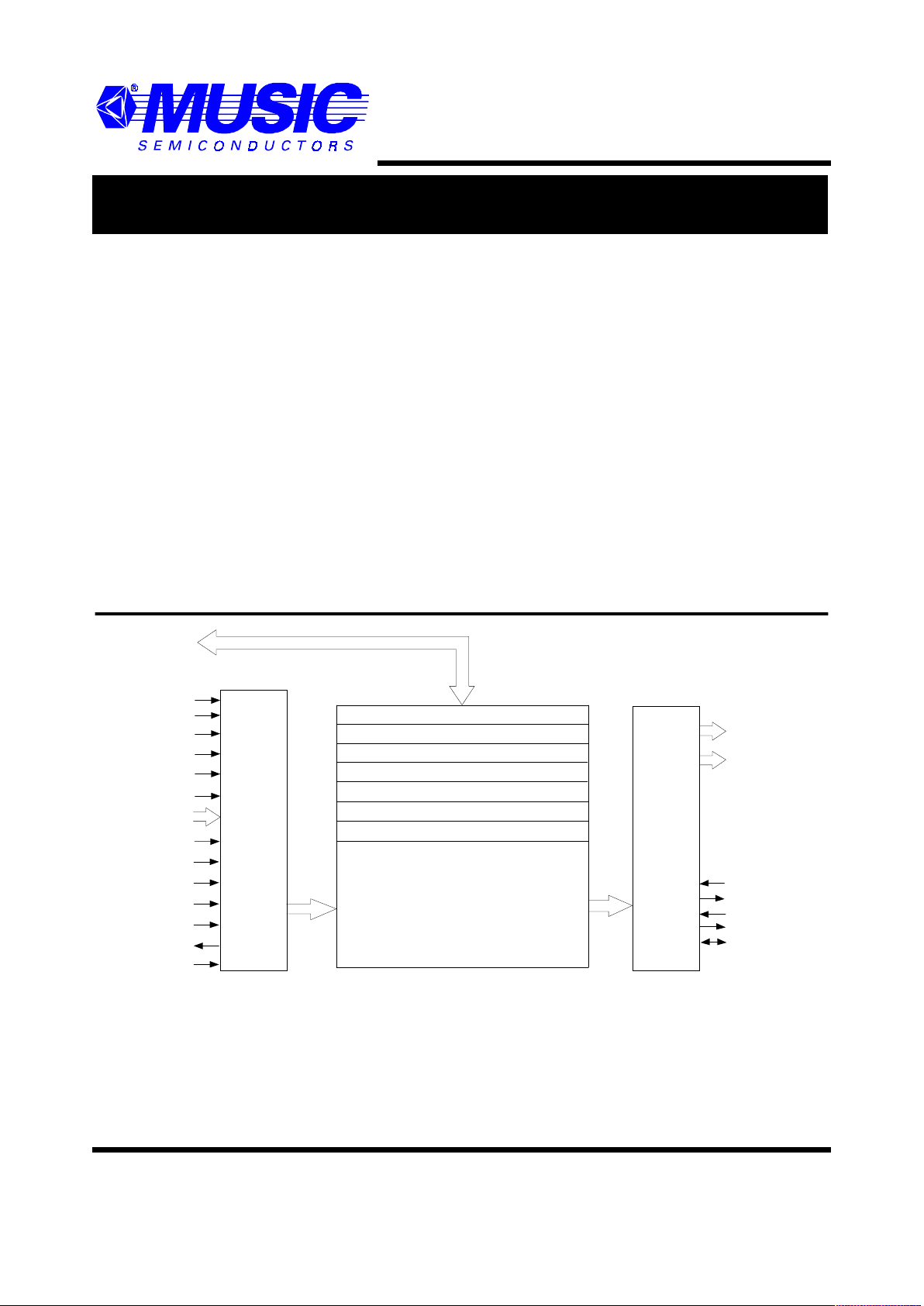
Figure 1: Blo ck Diagram
DQ31–0
/VB
AA Bus
PA3–0
/MM
/RESET
TCLK
TMS
TDI
TDO
/TRST
CONTROL
AND
ADDRESS
DECODER
PRIORITY
ENCODER
AND
FLAG
LOGIC
/E
/CS1
/CS2
/W
/OE
/AV
AC Bus
/DSC
INSTRUCTION REGISTER
DEVICE SELECT REGISTER
STATUS REGISTER
CONFIGURATION REGISTER
ADDRESS REGISTER
MASK REGISTERS 1–7
COMPARAND REGISTER
4 K x 64 Word
(MUAC4K64)
8 K x 64 Word
(MUAC8K64)
Address Database
/M F
/MI
/FF
/FI
MUAC Routing CoProcessor (RCP) Family
MUAC Routing CoProcessor (RCP) FamilyMUAC Routing CoProcessor (RCP) Family
MUAC Routing CoProcessor (RCP) Family

MUAC Routing CoProcessor (RCP) Family General Description
2
Rev. 4a
GENERAL DESCRIPTION
The MUAC RCP family consists of 4K and 8K x 64-bit
Routing CoProcessors (RCPs) with a 32-bit wide data
interface and a 32-bit ternary compare instruction. The
device is designed for use in layer 3 switches, routers, and
layer 2 switches to provide very high throughput address
translation using tables held in external RAM. The MUAC
RCP has a fully deterministic search time, independent of
the size of the list and the position of the data in the list.
This unique feature guarantees that the wire speed address
recognition does not impact the latency or induce some
jitter on the latency of the global system. Address fields
from the packet header are compared against a list of
entries stored in the array. As a result of the comparison,
the MUAC RCP generates an index that is used to access
an external RAM where port mapping data and other
associated information is stored.
A set of control states provides a powerful and flexible
control interface to the MUAC RCP. This control structure
allows memory read and write, register read and write,
data move, comparison, validity control, addressing
control, and initialization operations.
The MUAC RCP architecture uses direct hardware control
of the device and an independent bus for returning match
results. Software control is also supported for systems
where maximum performance is not needed.
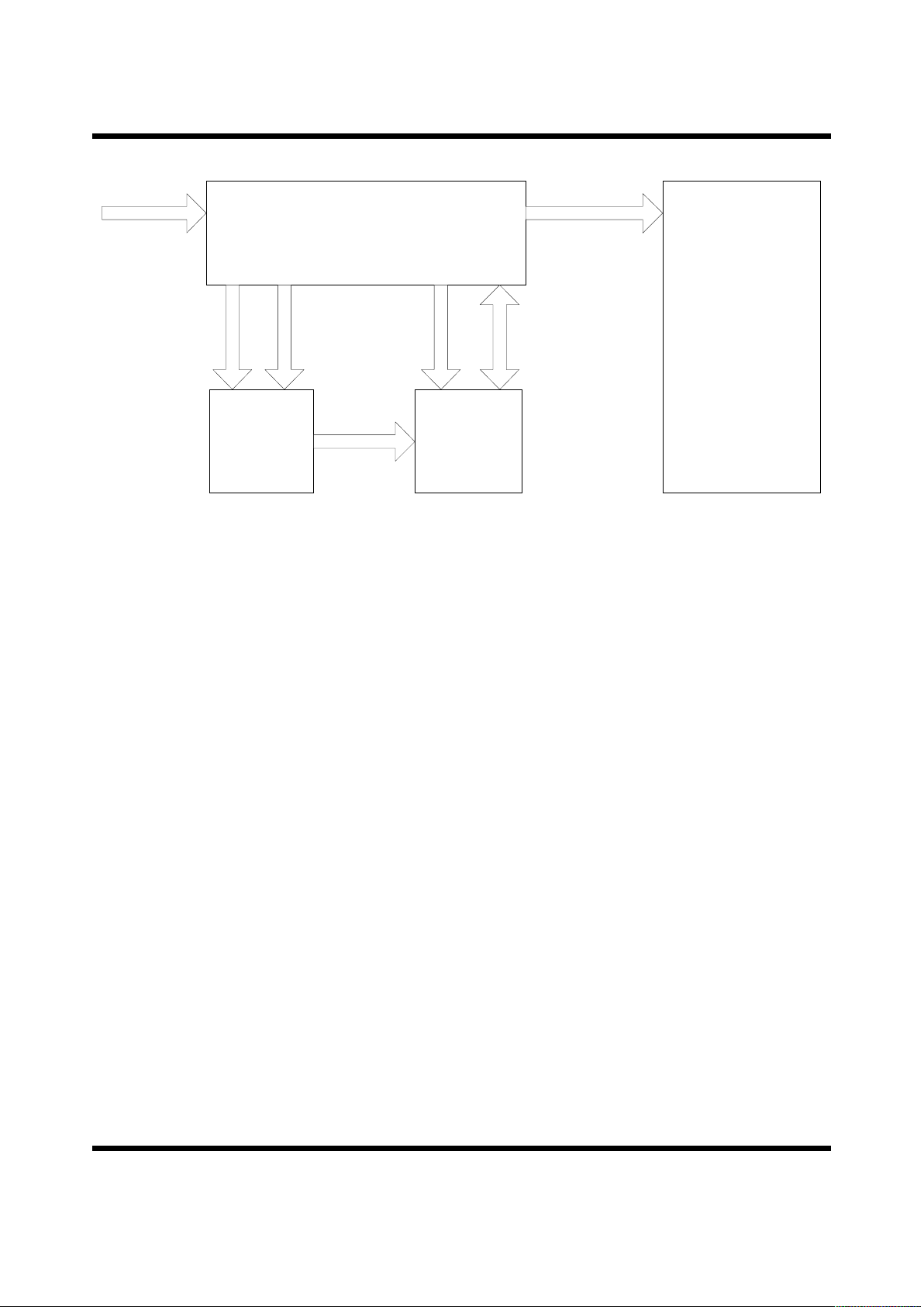
OPERATIONAL OVERVIEW
The MUAC RCP is designed to act as an address
translator for lookup tables in layer 3 switches, routers,
and layer 2 switches. Refer to Figure 2 for a simplified
block diagram of a switch. During normal operation, the
controller extracts the address information from an
arriving packet to form the comparand, which is then
compared against the contents of the MUAC RCP. The
MUAC RCP generates an index that is used to access the
data in an external RAM, which holds the destination port
for accessing the network. The controller reads the data
from the RAM and forwards the packet.
A unique feature of the MUAC RCP is its ternary
comparison that processes IPv4 CIDR addresses in a
single cycle. The bits of each MUAC RCP word are
paired, such that each pair can contain two binary values
(0,1) or one ternary (0,1,X= “Don’t Care”) value. A
ternary value uses two bits, pairing bit n from the first 32
bits (31-0) with bit n+32. When storing a ternary 0 or 1,
the value to be stored is written into bit n (0<=n<=31), and
the complement of the value is written to bit n+32. Thus, a
ternary 0 written to ternary pair 7 would consist of a 0
stored in bit 7 and a 1 stored in bit 39. When storing a
ternary X, 0 is written to both bits in the pair.
Using bit pairs that are 32 bits apart simplifies the
computation of the pair by a processor. Assume that the
ternary value we wish to store is contained in two 32-bit
processor words. Word A contains the value to be stored
and word M contains a mask value, with a 0 in each
position at which an X is to be stored. The value to be
written to bits 31-0 of the MUAC RCP is (A&M) and the
value to be written to bits 63-32 of the MUAC RCP is
(~A&M).
A special instruction, CMPT DQ, performs the ternary
comparison processing for IPv4 CIDR addresses. The data
on the DQ bus are used directly as both the comparand and
compare mask bits 31–0, and the one’s complement of the
DQ bus data are used as both the comparand and compare
mask bits 63–32. As a result, this instruction matches a
DQ bit of 0 with bit pairs storing both 0 and X, and a DQ
bit of 1 matches bit pairs storing both 1 and X.
IPv4 CIDR addresses are prioritized by placing their
ternary-encoded values into the MUAC RCP memory
such that entries with longer netmasks (longer matches)
have higher priority (lower indices). Thus, when the
MUAC RCP performs a ternary comparison, it will return
the index of the longest matching entry. Typically, the
system is initialized by a processor that writes routing
table information into the MUAC RCP. The index at
which a write takes place is driven onto the PA:AA bus, so
that output port data can be written simultaneously into the
external RAM at the correct index.
The validity of a location in the Address Database is
determined by an extra bit called the Validity bit. This bit is
set and reset either with an index or an associative match.
Therefore, when a new entry is written to the database, its
Validity bit is set valid.
When a database location is deleted, the Validity bit for that
entry is reset, and the index of the location is driven onto
the Active Address bus. This simple mechanism allows
easy maintenance of the tables in both the database and the
external RAM.
The MUAC RCP supports simple daisy chained vertical
cascading that serves to prioritize multiple devices and
provides system-level match and full indication. If the
slight timing overhead associated with the daisy chain is
unacceptable, the MUAC RCP is designed to facilitate
external prioritization across multiple devices.
For layer 2 applications, the MAC addresses are processed
in a binary mode, and the MUAC RCP looks for an exact
match. An MUAC RCP can be used to process both MAC
addresses and IPv4 CIDR in the same device.
Operational Overview MUAC Routing CoProcessor (RCP) Family
Rev. 4a 3
Figure 2: Switch Block Diagram
Controller
RAM
Switch
Fabric
MUAC
Switch Control
and Packet
Data
Network
Address
Data
RCP
Control
Packet Stream
RAM
Address

MUAC Routing CoProcessor (RCP) F a mi ly Pin Descriptions
4
Rev. 4a
PIN DESCRIPTIONS
Note: Signal names that start with a slash (“/”) are active LOW. All signals are 3.3V CMOS level. Never leave inputs floating. The
CAM architecture draws large currents during compare operations, mandating the use of good layout and bypassing techniques. Refer
to the Electrical Characteristics section for more information.
DQ31–0 (Data Bus , Three -s ta te , C om m on
Input/ Outpu t)
The DQ31–0 lines convey data to and from the MUAC
RCP. When the /E input is HIGH the DQ31–0 lines are
held in their high-impedance state. The /W input
determines whether data flows to or from the device on the
DQ31–0 lines. The source or destination of the data is
determined by the AC bus, DSC, and the /AV line. During
a Write cycle, data on the DQ31–0 lines is registered by
the falling edge of /E.
AC12–0/AC11–0 (Address/Control Bus,
Input)
When Hardware control is selected, the AC bus conveys
address or control information to the MUAC RCP,
depending on the state of the /AV input. When /AV is
LOW then the AC bus carries an address; when /AV is
HIGH the AC bus carries control information. Data on the
AC bus is registered by the falling edge of /E. When
software control is selected, the state of the AC bus does
not affect the operation of the device.
DSC (Data Segment Control, Input)
When DQ bus access to a 64 bit register or memory word
is performed, the DSC input determines whether bits 31–0
(DSC LOW) or bits 63–32 (DSC HIGH) are accessed.
Access to 32 bit registers require that DSC be held LOW.
AA12–0/AA11–0 (A ctive Add r ess, Outp ut)
The AA bus conveys the Match address, the Next Free
address, or Random Access address, depending on the
most recent memory cycle. The /OE input enables the AA
bus; when the /OE input is HIGH, the AA bus is in its
high-impedance state; when /OE is LOW the AA bus is
active. In a vertically cascaded system after a Comparison
cycle, Write at Next Free Address cycle or Read/Write at
Highest-Priority match, only the highest-priority device
will enable its AA bus, regardless of the state of the /OE
input. In the event of a mismatch in the Address Database
after a Compare cycle, or after a Write at Next Free
Address cycle into an already full system, the
lowest-priority device will drive the AA bus with all 1s.
The AA bus is latched when /E is LOW, and are free to
change only when /E is HIGH.
Figure 3: MUAC RCP Pinout
82
83
84
85
86
87
88
89
90
91
92
93
94
95
96
97
98
81
31
100
99
33
34
35
36
37
38
39
40
41
42
43
44
45
46
47
48
49
50
32
TCLK
TMS
TDI
DQ0
DQ1
DQ2
DQ3
VDD
DQ4
DQ5
DQ6
DQ7
VSS
DQ8
DQ9
DQ10
DQ11
VDD
DQ12
DQ13
DQ14
DQ15
VSS
VSS
VSS
AC11
AC10
AC9
AC8
AC7
AC6
VDD
AC5
AC4
AC3
AC2
AC1
AC0
TDO
AA12/NC*
80
79
78
77
76
75
74
73
72
71
70
69
68
67
66
65
64
63
62
61
60
59
58
57
56
55
54
53
52
51
DQ16
DQ17
DQ18
DQ19
VDD
DQ20
DQ21
DQ22
DQ23
VSS
DQ24
DQ25
DQ26
DQ27
VDD
DQ28
DQ29
DQ30
DQ31
VSS
/E
/W
/CS1
/CS2
/OE
VSS
/AV
/VB
RESET
/TRST
1
2
3
4
5
6
7
8
9
10
11
12
13
14
15
16
17
18
19
20
21
22
23
24
25
26
27
28
29
30
VSS
VSS
AA12/NC*
AA8
VSS
AA7
AA6
AA5
AA4
VDD
AA3
AA2
AA1
AA0
VSS
/MF
/FF
VDD
/M
I
/FI
VSS
/MM
DSC
PA3
PA2
PA1
PA0
AA10
AA9
AA11
MUAC RCP
100-Pin TQFP
(Top View)
* NC on MUAC4K6
4

Pin Descriptions MUAC Routing CoProcessor (RCP) Family
Rev. 4a 5
PA3–0 (Page Address, Output)
The PA3–0 lines convey Page Address information. When
the /OE input is HIGH, the PA3–0 outputs are in their
high-impedance state; when /OE is LOW the PA3–0 lines
carry the Page Address value held in the Configuration
register. The PA3–0 lines are latched when /E is LOW, and
are free to change only when /E is HIGH. The Page
Address value of the currently active or highest-priority
responding device is output at the same time, and under
the same conditions, as the AA bus is active.
/E (Chip Enable, Input)
The /E input is the main chip enable and synchronizing
control for the MUAC RCP. When /E is HIGH, the chip is
disabled and the DQ31–0 lines are held in their
high-impedance state. The falling edge of /E registers the
/W, /CS1, /CS2, /AV, /AC bus, DSC, and the /VB and
DQ31–0 lines for a Write cycle. /E being LOW causes the
results of the previous comparison or memory access to be
latched on the PA:AA bus; when /E goes HIGH the latches
opens allowing the new comparison results or random
access memory address to flow to the PA:AA bus.
/CS1, /CS2 (Chip Select 1, Chip Select 2,
Inputs)
The /CS1 and /CS2 inputs enable the MUAC RCP. If
either /CS1 or /CS2 are LOW, the device is selected for a
Read, Write, or Compare cycle through the DQ31–0 lines,
or for an internal data transfer. The /CS1 and /CS2 lines do
not have any effect on the PA:AA bus. The state of the
/CS1 and /CS2 lines is registered by the falling edge of /E.
/W (Wri te Enable, Inpu t)
The /W input determines the direction of data transfer on
the DQ31–0 lines during Read, Write, and Data Move
cycles. When /W is LOW, data flows into the DQ31–0
lines; when /W is HIGH, data flows out. The /W line also
conditions the control state present on the AC bus and
DSC lines. The state of the /W line is registered by the
falling edge of /E.
/OE (Output Enable, Input)
The /OE input enables the PA:AA bus. When /OE is
HIGH, PA:AA bus are in their high-impedance state.
When /OE is LOW, PA:AA bus are active, and convey the
results of the last Comparison Cycle Match address or
Memory Access address. In a vertically cascaded system,
only the PA:AA bus of the highest-priority device will be
activated by /OE being LOW; in lower-priority devices,
the PA:AA bus remains in high-impedance regardless of
the state of /OE.
/AV (Address Valid, Input)
When Hardware control is selected, the /AV input
determines whether the AC bus carries address or control
information. When /AV is LOW, the AC bus conveys a
memory address; when /AV is HIGH, the AC bus conveys
control information. The state of the /AV line is registered
by the falling edge of /E. When software control is
selected, the /AV line distinguishes between instructions
and data on the DQ31–0 lines; when /AV is LOW, data is
present on the DQ31–0 lines; when /AV is HIGH, an
instruction is present on the DQ11–0 lines.
/VB (Validity Bit, Three-state, Common
Input/Output)
During accesses over the DQ31–0 lines, the /VB line
conveys validity information to and from the MUAC RCP.
During a Write cycle (/W=LOW), when /VB is LOW the
addressed location is set valid; when /VB is HIGH it is set
empty. During a Read cycle (/W=HIGH), the validity of
the addressed location is read on the /VB line. During a
Write cycle, the state of the /VB line is registered by the
falling edge of /E.
/MF (Match Flag, Output)
The /MF output indicates whether a valid match has
occurred during the previous Comparison cycle. If the
/MF output is HIGH at the end of a Comparison cycle,
then no match occurred; if it is LOW then either a match
occurred within the device, or the /MI input is LOW,
conditioned by the /MF output from a higher-priority
device in the system. The state of the /MF line will not
change until after the rising edge of /E during the
Comparison cycle. Note that /MF indicates the results of
the most recent Comparison cycle; it will not change when
the PA:AA bus carry an address other than the Match
address.
/MI (Match Input, Input)
The /MI input receives match information from the next
higher-priority MUAC RCP in a vertically cascaded
system to provide system-level prioritization. When the
/MI input is HIGH, the /MF output will only go LOW if
there is a match during a Comparison cycle; when the /MI
input is LOW, the /MF output will go LOW. The /MF
output from one device is connected to the /MI input of the
next lower-priority device. The /MI pin of the
highest-priority device must be tied HIGH.

MUAC Routing CoProcessor (RCP) F a mi ly Pin Descriptions
6
Rev. 4a
/FF (Full Flag, Output)
The /FF output indicates when all the memory locations
have their Validity bits set valid (LOW). When there is at
least one location with its Validity bit set HIGH, the /FF
output will be HIGH; when all locations have their
Validity bits set LOW, and the /FI input is LOW, the /FF
output will be LOW. If the /FI input is HIGH, the /FF
output will be HIGH. The state of the /FF line will not
change until after the rising edge of /E during a Write
cycle.
/FI (Full Input, Input)
The /FI input receives full information from the next
higher-priority MUAC RCP in a vertically cascaded
system to provide system-level full information. When the
/FI input is LOW the /FF output will be HIGH if there is at
least one location whose Validity bit is set invalid; when
all locations have their Validity bits set valid, the /FF
output goes LOW. When the /FI input is HIGH, the /FF
output will remain HIGH. The /FF output from one device
is connected to the /FI input of the next lower-priority
device to give system-full indication. The /FI pin of the
highest-priority device must be tied LOW.
/MM (Multiple Match, Open Drain Output)
The /MM line indicates that there is a multiple match
within the system. When the /MI input is HIGH, the /MM
line is pulled LOW if there are at least two matches within
the MUAC RCP as a result of the previous Comparison
cycle; when there are less than two matches, the /MM line
floats HIGH. When the /MI input is LOW, the /MM line is
pulled LOW if there are one or more matches within the
MUAC RCP as a result of the previous Comparison cycle;
when there are no matches, the /MM line floats HIGH.
The /MM lines have open-drain outputs, so all /MM lines
within the system are connected together to give
system-level multiple match indication. The state of the
/MM line will not change until after the rising edge of /E
during a Comparison cycle.
/RESET
The /RESET input is used to reset the MUAC RCP to a
known state. When the /RESET line is pulled LOW it
causes the MUAC RCP to enter its reset state. After power
is applied to the MUAC RCP, the /RESET line must be
held LOW for a time equal to or greater than the minimum
RESET pulse width before the device can operate
correctly. This pin is internally pulled up.
TCLK (JT AG Test Clock, Input)
The TCLK input is the Test Clock input. This pin is
internally pulled up.
TMS (JTAG Test Mode Select, Input)
The TMS input is the Test Mode Select input. This pin is
internally pulled up.
TDI (JTAG Test Data Input, Input)
The TDI input is the Test Data input. This pin is internally
pulled up.
TDO (JTAG Test Data Output, Output)
The TCLK output is the Test Data Output. This pin is
internally pulled up.
/TRST (JTA G Reset, Input)
The /TRST input is the Reset input, and serves to reset the
Test Access Port circuitry to its reset condition. This pin is
internally pulled up.
VDD, VSS (Positive Power Supply, Ground)
These pins are the main power supply connections to the
MUAC RCP. VDD must be held at +3.3 Volts and ± 0.3
Volts relative to the VSS pin, which is at 0 Volts, system
reference potential, for correct operation of the device.
Note: The TCLK, TMS, TDI, TDO, and /TRST lines are defined
in the IEEE Standard Test Access Port and Boundary-scan
Architecture IEEE Standard. 1149.1-1990 and IEEE Standard.
1149.1a-1993.

Functional Description MUAC Routing CoProcessor (RCP) Family
Rev. 4a 7
FUNCTIONAL DESCRIPTION
Data is read from and written to the MUAC RCP through
the DQ31–0 lines. The Control bus, which is comprised of
Chip Enable (/E), two Chip Selects (/CS1, /CS2), Write
Enable (/W), Output Enable (/OE), Validity Bit Control
(/VB), Address Valid (/AV), Data Segment Control (DSC),
and the Address/Control inputs (AC bus) controls the
MUAC RCP. When the /AV line is LOW, the AC bus
carries an address for random access into the Memory
array; when it is HIGH, the AC bus conveys control
information. The MUAC RCP control states perform
Register Read/Write, Memory Read/Write, Data Move,
Comparison, Validity Bit Control, Initialization, and
Address Register Control. These functions are
summarized in Control State Overview on page 17.
Random access to memory locations occurs when the /AV
line is LOW; during a Write cycle, the validity of the
location is set by the /VB input. When the /AV line is
HIGH the control states allow read and write access to the
register set comprising Comparand register, seven mask
registers, a Configuration register, a Status register, an
Address register, a Device Select register, and an
Instruction register. The Configuration register sets the
persistent operating conditions of the device: the Page
address of the device, selection of mask register for
directly addressed memory writes, and selection between
hardware and software control.
When Hardware control is selected, control is through the
AC bus and DSC line. When Software control is selected,
control is through the Instruction register, which is loaded
from the DQ bus. Under software control the /AV line is
used to distinguish between data and an instruction on the
DQ bus. Therefore, in Software Control mode, random
access to the Memory array can take place only using
indirect addressing through the Address register.
The two Chip Select lines /CS1, /CS2 enable the device
and simplify access to a multi-chip system, if either Chip
Select line is LOW the device is selected. The MUAC
RCP also can be selected through the Device Select
register when its value is set to that of the Page address of
the device, and the enable bit in the Device Select register
is set LOW. The /OE input enables the output signal and is
used to synchronize devices in a multi-chip system, and to
prevent race conditions among devices during priority
resolution.
The output signals comprise the Active address (AA bus),
and the Page address (PA bus). The PA:AA bus provides
the current Active address, which is either the Match
address, Next Free address, or the Random Access
address, concatenated with the Device Page address. The
source of Active address is dependent on the previous
control state, allowing access to associated data in the
external RAM at the same location as an access in the
MUAC RCP for all types of cycles.
The Output enable, /OE, controls the PA:AA bus: when it
is LOW after a Compare cycle, the highest-priority
responding device outputs its Page and Match addresses
on PA:AA bus. Only the highest-priority responding
device is enabled, all other lower-priority devices will
have their PA:AA bus in the high-impedance state,
regardless of the state of their respective /OE lines: when
/OE is HIGH, the PA:AA remain in the high-impedance
state.
When a mismatch occurs in the system, the lowest-priority
device, as defined in the Configuration register, will drive
the PA:AA bus with all 1s. When any Read or Write cycle
occurs, the address of the accessed location is output on
the PA:AA bus. The address output on the PA:AA bus is
persistent, and is held latched until /E goes HIGH during
the next cycle that changes the Active address. The PA:AA
bus is free to change only while /E is HIGH. Once /E goes
LOW, the state of the PA:AA bus is latched.
After a Compare cycle, the /MF and /MM flags are free to
change after /E has gone HIGH. Once the Match Flag
daisy chain has resolved device prioritization, the /OE
lines can be asserted to enable the PA:AA bus from the
highest-priority matching device.
In a multi-chip system, when a device remains deselected
during a Compare cycle through /CS1 and /CS2 being
HIGH and there being no match between the Device
Select register and the Page Address register, that device
will clear any previous positive match results. In other
words, if it had previously been indicating a match from
an earlier Comparison cycle, it will now be set to indicate
a mismatch, even though it was not selected during the
most recent Compare cycle.
For pure software control of the MUAC RCP, instructions
can be loaded into the Instruction register, and results read
from the Status register. The Status register holds the
results of comparison: PA:AA bus, /MF, /FF, and /MM
plus two PA:AA Validation bits that indicate the type of
cycle that generated the PA:AA bus value.
Vertical cascading is supported through a daisy chain
architecture. There are two daisy chains, one each for the
Match flag and the Full flag; the Multiple Match flag is
connected between devices through an open-drain line.
The Match flag (/MF) from a higher-priority device is
connected to the Match input (/MI) of the next
lower-priority device to provide prioritization throughout
a multiple device system. The /MF output from the

MUAC Routing CoProcessor (RCP) Family Operational Characteristics
8
Rev. 4a
lowest-priority device provides a system Match flag. If the
delay through the daisy chain is unacceptable, the /OE
input can be used by external priority-resolution circuitry
to enable the highest-priority responder in the system.
The match conditions on the Match and Multiple Match
flag lines are persistent indicating the results of the most
recent Compare cycle. The Match flags are free to change
after the rising edge of /E during a Compare cycle, at
which time the daisy chain starts to resolve device
prioritization. Once the daisy chain has settled, the /OE
lines can be pulled LOW to access the Highest-Priority
Match address on the PA:AA bus.
The Multiple Match open-drain output (/MM) provides
multiple match indication when there are two or more
matches in a single device, or a device has its /MI input
LOW and has a match; the /MM flags of all devices in the
system are wire-ORed. Multiple responders can be
accessed sequentially by resetting the Highest-Priority
Match latch with the control state Advance to Next
Matching Location.
The Full flag (/FF) is cascaded from one device to the Full
Flag input (/FI) of the next lower-priority device in the
system. The /FF output from the lowest-priority device
provides a system Full flag. The Full flag is free to change
after the rising edge of /E during a Write cycle. The daisy
chains are persistent and are not conditioned by the /OE
input.
The MUAC RCP supports JTAG boundary-scan testing
through the pins TCK, TMS, TDI, TDO, and /TRST,
according to the IEEE 1149 Standard: Test Access Port
and Boundary-scan Architecture.
OPERATIONAL CHARACTERISTICS
Processor Interface
The processor interface is through a 32-bit data bus
DQ31–0 and control signals comprised of Chip Enable
(/E), two Chip Selects (/CS1, /CS2), Write Enable (/W),
Output Enable (/OE), Validity Bit Control (/VB), Address
Valid (/AV), Data Segment Control (DSC), and
Address/Control inputs (AC bus). When the /AV line is
LOW, the DSC and AC bus carries an address for random
access into the Memory array; when it is HIGH, the AC
bus conveys control information.
Most of the functionality of the MUAC RCP is accessed
through the control states on DSC and AC bus when /AV
is HIGH. The processor maps the control structure into
memory space and controls the MUAC RCP through
memory Read and Write cycles. Using this memory
mapping scheme, the /AV line should be driven from logic
that generates a HIGH level within the mapped range of
the control states, and a LOW level outside it. Other
control inputs /E, /W, /CS1, and /CS2 are analogous to
SRAM control inputs.
The /VB line acts like an extra data bit during memory
Read and Write cycles and is used to read and write the
validity of any memory location.
The MUAC RCP is enabled either through hardware
through /CS1 or /CS2 being LOW, or it is enabled by the
value written to the Device Select register matching with
the Page Address field of the Configuration register. One
extra bit in the Device Select register enables the
comparison between the Page Address value and the
Device Select register. These Chip Select mechanisms
operate in parallel. If any one is active, the device is
enabled.
The MUAC RCP can be controlled directly through
software. The Software Control mode is selected through
settings in the Configuration register.
When the Software Control mode is selected, control
states are written to the Instruction register from DQ11–0
during a Write cycle with the /AV line held HIGH. DQ12
acts as the DSC input. If the control state does not involve
any data transaction on the DQ31–0 lines, the instruction
is executed during the same cycle; the state of DQ13
modifies the instruction, its state is equivalent to the /W
input.
Note: It is up to the system designer to ensure that the correct
cycle type follows the loading of an instruction in Software
Control mode. If the instruction expects a Read cycle, and a
Write cycle is executed, or vice versa, the function of the MUAC
RCP is undefined. Such an error may lead to data loss, but will
not damage the device physically.
A Read cycle with the /AV line HIGH will access the
Status register, allowing results to be read back without
loading a new instruction. After a Comparison cycle,
Write at Next Free Address cycle or Read/Write at
Highest-Priority match in a vertically cascaded system,
only the highest-priority device will enable its DQ31–0
lines and output the contents of its Status register. After a
Comparison cycle, in the event of a mismatch in the
MUAC, the DQ31–0 lines of the lowest-priority device
will be enabled. After a random access Read or Write
cycle, the Status register of any selected device will be
enabled. Under these circumstances, it is up to the user to
ensure that only a single device is enabled through /CS1,
/CS2, or the Device Select register.

Operational Characteristics MUAC Routing CoProcessor (RCP) Family
Rev. 4a 9
The instruction is persistent, so that all subsequent data
transactions will be executed according to the control state
held in the Instruction register. The results of a
Comparison cycle can be read back from the Status
register, and include PA:AA bus, /MF, /MM, and /FF. The
following sequence of events provides the fastest
operation of the MUAC RCP in Software Control mode:
Note: It is up to the system designer to ensure that the correct
cycle type follows the loading of an instruction in Software
Control mode. If the instruction expects a Read cycle, and a
Write cycle is executed, or vice versa, the function of the MUAC
RCP is undefined. Such an error may lead to data loss, but will
not damage the device physically.
Hardware Control
Direct hardware control using the AC bus and DSC line
enhances performance of the MUAC RCP. The AC bus
inputs determine which CAM location is accessed, and the
DSC determines whether bits 31–0 (DSC LOW) or bits
63–32 (DSC HIGH) are active. The Hardware Control
mode is selected when Configuration Register bits
FR27–26 are set LOW. The AC bus inputs are qualified by
/W, /AV, and /VB. When /AV is LOW, the AC bus and
DSC line carry the address for a random Read or Write
cycle, depending on the state of /W, and /VB carries the
validity of the location. During a Write cycle, /VB is
written to the Validity bit of the addressed location; during
a Read cycle, the validity of the location is read on the /VB
line. When /VB is LOW, the location contains valid data;
when /VB is HIGH the location is empty.
When /AV is HIGH, the AC bus and DSC line carry
address and control information. The DSC line selects
whether bits 31–0 (DSC LOW) or bits 63–32 (DSC
HIGH) participate in the operation. The AC8–6 lines
select the mask register and the AC5–0 lines provide the
Op-Code. If masking is not used, and all random
addressing of the memory is indirect through the Address
register, then only the DSC and AC5–0 lines are needed
for full control of the device.
In applications where a restricted number of control lines
are available, or where speed is not critical, the MUAC
RCP can be controlled in Software Control mode where
the control states are loaded into the Instruction register
through the DQ31–0 lines. The control states are identical
in both Hardware and Software Control modes, although
DQ12 and DQ13 take on special significance in Software
mode.
Software Control
For optimum performance, the AC bus and DSC line
control the MUAC RCP, allowing data transactions
through the DQ31–0 lines during a control cycle. In cases
where the overhead of a separate data load cycle can be
accommodated, the MUAC RCP can be operated through
the Instruction register. The AC bus and DSC line are not
used.
Control through the Instruction register is selected by the
FR27–26 bits of the Configuration register being set
HIGH. The instruction is loaded from the DQ11–0 lines
(with DSC on DQ12) into the Instruction register during a
Write cycle with the /AV line HIGH. The instructions are
directly analogous to the control states for any operation
that does not involve data transfer on the DQ31–0 lines, in
which case the instruction is executed during the same
cycle as the instruction is loaded. To distinguish between
Read and Write control states, DQ13 is used to indicate
which type of instruction should be executed. When DQ13
is LOW at the beginning of the cycle, the instruction
executed is the Write Cycle instruction (/W = LOW when
control state is conveyed on AC bus and DSC); when
DQ13 is HIGH at the beginning of the cycle, the
instruction executed is the Read Cycle instruction (/W =
HIGH when control state is conveyed on the AC bus).
When the instruction calls for data to be written or read
from the DQ31–0 lines, the instruction is loaded into the
Instruction register during the cycle, and the next Data
Read or Write cycle with /AV LOW executes the
instruction using the DQ31–0 bus for the data transaction.
The instruction is persistent; for example, if no other
instruction is loaded into the Instruction Register,
subsequent data transactions with the /AV line LOW will
be executed according to the instruction currently loaded
in the Instruction register. When there is a data access to a
memory location on DQ31–0 associated with the
instruction, the /VB line carries the validity of that
location.
Instructions that involve data transactions on DQ31–0, and
are therefore executed on a subsequent Read or Write
cycle with the /AV line LOW, are all Read/Write Memory
and Read/Write Register instructions, Read Validity, Write
PA3-0. All other instructions are executed in a single cycle
with the state of DQ13 being interpreted as the state of the
/W line during the equivalent hardware control state.
For Read Cycles with the /AV line HIGH, there is a
Software Control mode. This mode is selected through the
Configuration bits FR27–26. In Software Control mode
(FR27–26 = 0b11) a Read cycle with /AV HIGH accesses
the Status register.
/AV Operation
1 Load ‘Compare DQ with CAM’ instruction
0 Comparand on DQ31–0
1 Read Status register
0 Next Comparan d on DQ31–0
1 Read Status register, etc.

MUAC Routing CoProcessor (RCP) Family Operational Characteristics
10
Rev. 4a
Active Address Interface PA:AA Bus
The Active Address interface PA:AA bus carries the
currently active address. The address source depends on
the most recent control state that caused it to change. The
possible address sources that are output on PA:AA bus are:
Highest-Priority Match address, Next Free address, Read
address, and Write address.
PA:AA Bus After a Comparison Cycle
After a Comparison cycle, or access to the
Highest-Priority address, the PA:AA bus carries one of the
following two possible results:
• The Match address if the Comparison cycle resulted
in a match in the MUAC. Only the device containing
the highest-priority match enables its PA:AA bus. All
other devices with either no match or a lower-priority
match, as indicated by the Match Flag daisy chain,
keep their PA:AA bus in high-impedance regardless
of the state of their /OE inputs.
• All 1s if there was no match in the MUAC. The
lowest-priority device, as indicated by bit FR25 in the
Configuration register, enables its PA:AA bus and
provides the source of all 1s. All other devices will
keep their PA:AA bus in high-impedance regardless
of the state of their /OE inputs.
PA:AA Bus After a Write at Next Free Address Cycle
After a Write at Next Free Address cycle the PA:AA
carries the address that was written to during that cycle.
Only the device in which the write occurred enables its
PA:AA bus. All other devices keep their PA:AA bus in
high-impedance regardless of the state of their /OE inputs.
In the event that the system was full prior to the Write at
Next Free Address cycle being executed, so that the write
operation was suppressed, the PA:AA carries all 1s. The
lowest-priority device, as indicated by bit FR25 in the
Configuration register, enables its PA:AA bus and
provides the source of all 1s. All other devices keep their
PA:AA in high-impedance regardless of the state of their
/OE inputs.
PA:AA Bus After a Random Access Read or Write to
the CAM
After a random Read or Write cycle to the MUAC, the
PA:AA bus carries the address that was accessed during
that cycle. Only the device in which the access occurred
enables its PA:AA bus. All other devices keep their
PA:AA bus in high-impedance regardless of the state of
their /OE inputs. Note that the access to the PA:AA bus
differs in this respect from the operation of the Status
register, which is accessible in any selected device under
this particular circumstance.
In the event that the Write cycle was broadcast to multiple
devices, all devices that have their /OE lines held LOW
will enable their PA:AA bus. Under this circumstance, it is
up to the system designer to ensure that only one /OE line
is driven LOW to prevent bus contention on the PA:AA
bus.
PA:AA Bus Conditions of Operation
• During a control state that does not have any effect on
the device address, such as a Write Register cycle, the
PA:AA bus remains unchanged. In other words, the
state of the PA:AA bus persists until another cycle
causes it to change.
• When enabled by /OE being LOW, the PA:AA bus is
only free to change while /E is HIGH. When /E goes
LOW the PA:AA bus is latched.
• The PA:AA bus is enabled when /OE is LOW
provided that the previous cycle causes them to be
active. When /OE is HIGH, the PA:AA bus is in
high-impedance. Note that /OE is asynchronous with
respect to /E, and is independent of Chip Select from
either /CS1, /CS2, or through the Device Select
register, except in the case of non-broadcast random
Read and Write cycles to the MUAC.
 Loading...