MUSIC MU9C8338A Datasheet

MU9C8338A Evalu ation Kit Users Manual
MU9C8338A Evalu ation Kit Users Manual
MU9C8338A Evalu ation Kit Users ManualMU9C8338A Evalu ation Kit Users Manual
BILL OF MATERIALS
The kit should contain the following:
• Evaluation board PCB
• 5v power-supply unit and power cord
• 25-pin D-type parallel port cable
•Data CD
• This manual
• CAMView LANCAM Viewer Manual
INTRODUCTION
Data Sheet Draft
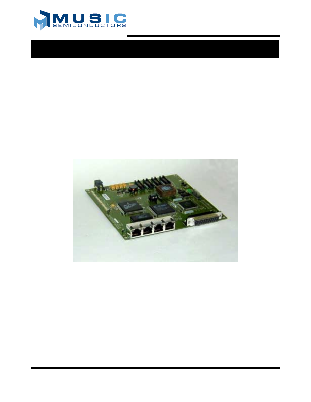
Figure 1: MU9C8338A Evaluation Board
The Evaluation board is shown in Figure 1. It is a very
simple printed circuit board that will allow a user to
evaluate the MUSIC Semiconductors MU9C8338A
Ethernet Filter device. The user simply plugs the board
into a standard PC printer port using the 25-pin connector
supplied. Sample C-Code functions and a demo program
are provided that allows the user to perform the following
tasks:
• Initialize the MU9C8338A and LANCAM
• Read and write internal registers
• Read the LANCAM contents
• Delete LANCAM entries
MUSIC Semiconductors, the MUSIC logo, and the phrase "MUSIC Semiconductors" are May 1, 2001 Rev. 0.2 Draft
Registered tr ademarks of MUSIC Semiconductors. MUSIC is a trademark of
MUSIC Semiconductors.
• Write permanent entries to the LANCAM
• Invoke the Purge routine using the software registers
or INCR pin
• View the data recently transmitted from the hardware
Result Port or Tag port
A simple Windows Software Tool is also provided that
allows the user to view instantly the contents of the
LANCAM database. This tool is called the CAMView
LANCAM Viewer and allows the user to view all or some
of the entries in the device. This can be used in
conjunction with the users own C-Code to play with the
MU9C8338A and view the additions and modifications to
the LANCAM database.

MU9C8338A Evaluation Kit Users Manual Hardware Installation
The user may also view any of the device signals by
connecting a logic analyzer to the board. Four
MICTOR-38 high-density connectors are provided that
will allow the user access to the signals. The connectors
are widely used by many logic analyzer pods. Network
traffic can be received by the MU9C8338A through the
RJ-45 connector shown in Figure 2. This enables the user
to send packets and then observe how the device parses
and deals with the Ethernet address information.
HARDWARE INSTALLATION
The Evaluation board is installed in the following way:
1. Remove the power supply unit and cable from the box.
Plug the power supply cable into the power supply unit.
The other end of the cable can be plugged into a
standard 110V outlet. Don’t plug the output connector
into the Evaluation Board for the moment.
2. Remove the 25-pin D-type parallel port connector from
the box. Insert one end into the parallel port connector
in the back of the PC. The board should work with all
parallel port configurations. It shouldn’t matter whether
the port is configured as PS-2, EPP or ECP. The only
stipulation is that the port is capable of bi-directional
data transfer. The base address of the port being used
should be set in any C-Code.
3. Carefully remove the Evaluation board from the
anti-static bag and place on an anti-static surface. It is
advisable that the Evaluation board is used in a lab
environment, where the board can be placed on an
anti-static surface on a work-bench. If this is not
possible, it is important that the board is laid flat on a
desk or table. It is very important that metal objects
should be kept away from the board as they may cause
short circuits in the metal circuit tracks. The board is
supplied with rubber insulating feet applied to the
bottom. These may be removed by hand if the user
wished to lie the board completely flat.
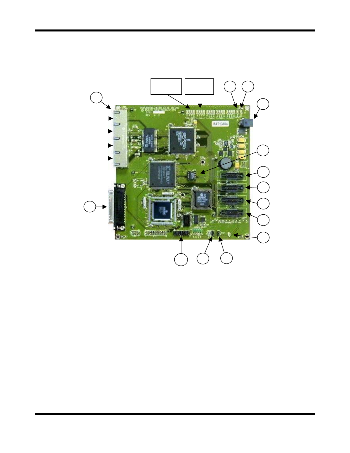
4. Make sure the FPGA data PROM is correctly installed
in socket U10 (see Figure 2 for location).
5. Plug the other end of the parallel port connector into P1
(see Figure 2 for location).
6. Connect the other end of the power supply unit into the
connector J1 (see Figure 2 for location).
7. If the power supply unit is plugged in correctly at the
power socket, two green LEDs D24 and D25 should
now be lit and the red D1 should be flashing (see Figure
2 for location).
8. If D1 is not flashing remove the power cord from J1
and check the data PROM in located properly in socket
U10. If neither of the green LEDs D24 and D25 is lit,
unplug the power supply cord and test the output with
an electrical meter. The output should be approximately
5v DC.
9. If you are still having problems installing the board,
please call MUSIC Semiconductors.
10.When the power is applied, the Result and Tag port
LEDs (see Figure 2 for location) should perform a
self-test and flash a few times. This will allow you to
check that all these LEDs are operational. The LED
self-test jumper (JP9) must be closed or the LEDs will
remain off.
11.If there was no problems, the LEDs should be lit as
described earlier, and you are now ready to use the
Evaluation board. Instructions about how the C-Code
and the Windows Software Tool is installed can be
found in the Software Installation section.
SOFTWARE INSTALLATION
The Evaluation board is supplied with some sample
C-Code, a Windows Software tool, documentation and
some design information. The design information is the
schematics, which are provided in Orcad Capture Version
7.2 format, the FPGA files, and the Verilog code for the
FPGA.
The software is provided on a data CD labeled
"MU9C8338A Evaluation Kit". The CD contains two
setup executable files. One will install the CAMView
LANCAM Viewer and the other will install the C-Code,
schematics, FPGA binary files, and associated
documentation. The CAMView Setup.exe file is located in
the CAMView directory. The installation process for the
LANCAM Viewer is described in detail in a separate
manual. This manual is titled "CAMView LANCAM
Viewer User Manual" and should be found in the Kit along
with this manual. The manual will describe how to install
the Windows Software and how it should be used.
The installation process which installs the C-Code,
documentation, and CAD files is as follows:
1. Insert the data CD titled: "MU9C8338A Evaluation
Kit" in the CD drive.
2. Press the Windows START button and select "Run".
Use "Browse" to select the "Setup.exe" file on the CD.
Click "OK". Alternatively use "Windows Explorer" to
locate the "Setup.exe" file from the CD drive. Once it is
located, double click on the icon.
3. An Install window will pop up that has the title
"MU9C8338A Evaluation Kit". Inside this there will be
a smaller "Welcome" window. Press "Next" to
continue.
2 Rev. 0.2 Draft

Software Installation MU9C8338A Evaluation Kit Users Manual
4. An Install window will pop up that has the title
"MU9C8338A Evaluation Kit". Inside this there will be
a smaller "Welcome" window. Press "Next" to
continue.
5. A "User Information" window will prompt you for your
name and Company name. Enter this information if not
automatically entered and press "Next".
6. A "Choose Destination Location" window will prompt
you to specify the default directory for all the files that
will be copied to your computer. You can either leave
this directory as the default shown or use the "Browse"
button to specify another. Once you are ready, press
"Next" to continue.
7. A "Select Program Folder" window will inform you
8. A "Start Copying Files" window will prompt you to
press "Next" to start copying files and thus finish the
installation. Press "Next" to continue. This will copy all
of the files to your hard disk.
9. A "Setup Complete" window will inform you that the
installation has finished. Press "Finish" to complete the
setup.
Once the installation is complete the following files should
have been copied to your hard disk. The default for the
<INSTALL_DIR> is C:\MUSICSemi\Hardware. You may
have changed this during the installation process. If it has
been changed, substitute the new home directory where
<INSTALL_DIR> is shown. The files and their paths are
shown in Tables 1 through 5.
that a new program folder will be created. You can
either leave this folder as shown or change the settings.
Once you are ready, press "Next" to continue.
Table 1: C-Code Files
Path Description
<INSTALL_DIR>\C_Code\Filter.h Header file that contains all the register defines and functions
<INSTALL_DIR>\C_Code\Demo.c Demo file that w ill allow the user to perf orm some basic operati ons
<INSTALL_DIR>\C_Code\Skeleton.c File that shows the basic operation of the board
<INSTALL_DIR>\C_Code\Clear.c File that contains a simple Clear Screen function
Table 2: Documentation Files
Path Description
<INSTALL_DIR>\Docs\8338AEval.pdf This Manual
<INSTALL_DIR>\Docs\8338A Data Sheet.pdf The data sheet for the MU9C8338A
<INSTALL_DIR>\Docs\8338Aerrat a.pdf An errata showing some bugs present in the MU9C 8338A
<INSTALL_DIR>\Docs\AN-N38.pdf An Application note showing how to use the MU9 C8338A
<INSTALL_DIR>\Docs\ AN-N34.pdf An Application note showing how to use the MU9C8338A with the
MPC860 processor
Table 3: Schematic Files
Path Description
<INSTALL_DIR>\Schematics\Eval8358V1.2.dsn The Schematics design file
<INSTALL_DIR>\Schematics\Eval8358V1.2.opj The Schematics OPJ file
Rev. 0.2 Draft 3

MU9C8338A Evaluation Kit Users Manual Software Installation
Table 4: Verilog Code
Path Description
<INSTALL_DIR>\Verilog\bufg.v Clock buffer file
<INSTALL_DIR>\Verilog\clk.v Clock divider
<INSTALL_DIR>\Verilog\dp_fifo.v FIFO used to store Result port entries
<INSTALL_DIR>\Verilog\epp.v Par allel port interface
<INSTALL_DIR>\Verilog\fstat.v Fifo entry counter
<INSTALL_DIR>\Verilog\led.v LED control for heartbeat, Result port and Tag port LEDs
<INSTALL_DIR>\Verilog\phy.v PHY register serial access interface
<INSTALL_DIR>\Verilog\phy _led.v LED control for the PHY LEDs
<INSTALL_DIR>\Verilog\proc.v The MU9C8338A processor port interf ace
<INSTALL_DIR>\Verilog\reg.v The FPGA internal registers
<INSTALL_DIR>\Verilog\res.v The MU9C8338A Result port interface
<INSTALL_DIR>\Verilog\rst.v The reset circuit
<INSTALL_DIR>\Verilog\tag.v The MU9C8338A Tag port interface
<INSTALL_DIR>\Verilog\tag_fifo.v FIFO used to store Tag port entries
<INSTALL_DIR>\Verilog\top.v The top lev el module that wires all other modules together
<INSTALL_DIR>\Verilog\mu8338Ademo.v The pseudo pad layer
Table 5: FPGA Binary Files
Path Description
<INSTALL_DIR>\FPGA\8338A.ucf The FPGA constraints file
<INSTALL_DIR>\FPG A\8338AV1_0.bit The FPGA binary file used when down-loading the design into the FPGA.
<INSTALL_DIR>\FPGA\8338AV1_0.mcs The FPGA PRO M file. The version number may change with subsequent
<INSTALL_DIR>\FPGA\res_ra m .edn The edn file for the Result port FIFO memory
<INSTALL_DIR>\FPGA\tag_ram.edn The edn file for the Tag port FIFO memory
The version number may change with subsequent releases.
releases.
4 Rev. 0.2 Draft

Hardware MU9C8338A Evaluation Kit Users Manual
HARDWARE
The Evaluation Board has connectors that allow a logic
analyzer to probe all the signals on the board. There are
also some jumpers that allow the board to be configured or
Result
Port LEDs
U5
10/100 Mb/s
Ethernet Port
Do Not Use
Do Not Use
Do Not Use
P1
reset. LEDs are provided so that the user may quickly
determine the power, FPGA status, Result status, and TAG
port status. Figure 2 shows the location of all these items.
TAG Port
LEDs
D24 D25
J1
U10
U16
U15
U14
Figure 2: Jumper, Connector, and LED Positions
There are four RJ-45 connectors on the board. This is
because the board is also used with the MUSIC
Semiconductors MU9C8358L filter which is a 4-port
device. The user should only connect network traffic to the
port that is shown as "10/100 Mb/s Ethernet" in Figure 2.
Parallel Port
The Evaluation board is connected to a users PC by means
of the Parallel (or printer) port. The Windows GUI and the
C-Code provided assume as default that the Parallel port is
located at address 0x378. The Base Address pre-processor
definition in the Filter.h file may be changed to the address
of your port if it is not 0x378. The Windows GUI will
allow you to choose 0x278 or 0x378 as the Base Address.
If you have problems getting the C-Code or Software GUI
to operate with your Parallel port, please notify MUSIC
Semiconductors.
U13
D1
JP11
JP9
JP5
The Hardware in the Evaluation board is designed in such
a way that it should operate with any parallel port that is
able to perform bi-directional data operations. The
hardware uses the Parallel port in PS-2 mode and expects
the data to be passed using the standard 8-bit Parallel port
data bus. Therefore, it doesn’t matter whether the PC bios
has the port set to Standard, PS-2, EPP or ECP mode as it
should operate in all these modes.
The C-Code routines and the Windows GUI both use the
Standard Parallel port Data and Control registers to output
or input any data. One stipulation is that if the port is set to
ECP mode in the PC bios, the port’s ECR register must be
set to PS-2 mode. The Windows GUI will do this
automatically. Any user specific code must use the
Init_Parallel_Port function as shown in the Skeleton.c file.
This function sets the ECR register appropriately and sets
the control bus to the default values.
Rev. 0.2 Draft 5

MU9C8338A Evaluation Kit Users Manual Hardware
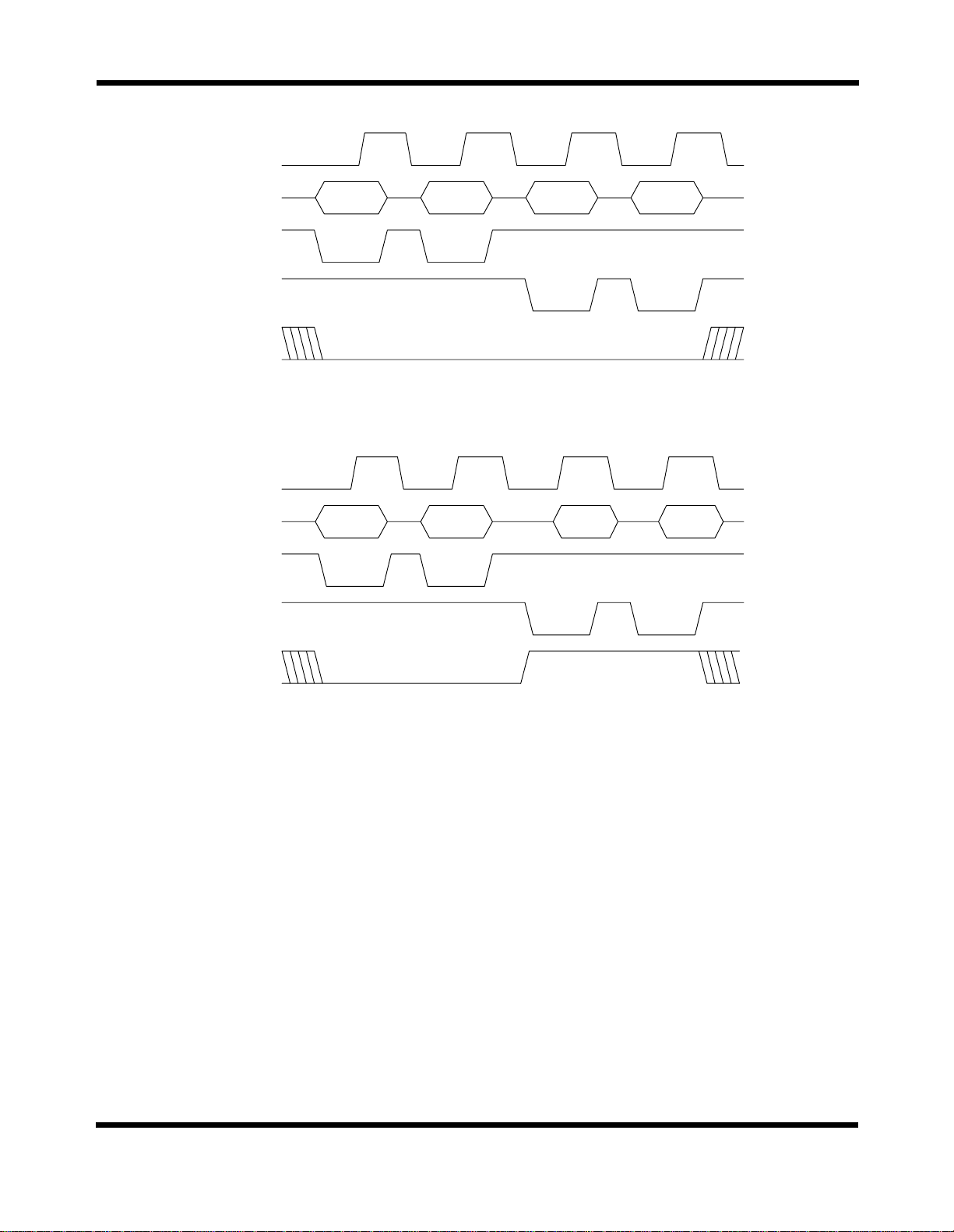
WAIT
DATA
ASb
DSb
WRITEb
WAIT
DATA
ASb
DSb
addr[7:0] addr[15:8] data[7:0] data[15:8]
WRITE CYCLES
addr[7:0] addr[15:8] data[7:0] data[15:8]
WRITEb
Figure 3: Parallel Port Read and Write Access
The Windows GUI and the C-Code functions transfer data
between the PC and the Evaluation board using four
consecutive 8-bit cycles. This allows a 16-bit address and
a 16-bit data word to be transferred. The FPGA expects a
read and write access to be as it is shown in Figure 3. The
Windows GUI, the reg_write, and reg_read functions use
the Parallel port’s Control register to assert the Address
Strobe (ASb), Data Strobe (DSb), and Write Strobe
(WRITEb) while read or writing the data using the 8-bit
data bus. The GUI and functions also monitor the port’s
Status register to detect the condition of the WAIT signal.
The write access uses two 8-bit address write cycles
followed by two 8-bit data write cycles. The read access
uses two 8-bit address write cycles followed by two 8-bit
data read cycles. Both accesses assert the appropriate
Strobe to indicate where it is an address or data cycle. The
FPGA completes a cycle by asserting its WAIT output.
There is two other Parallel port signals that are not directly
READ CYCLES
used for transferring data. These are the IRQb and INITb
signals. IRQb is a Parallel port input and is asserted low by
the Evaluation board when the MU9C8338A /INTR signal
is asserted low. It will return to its original state, which is
logic 1 once the /INTR output is returned to logic 1. The
user may monitor the state of the IRQb input with the
Poll_For_INTR function or configure their PC to use a
user-designed Interrupt Service Routine. The other signal
is the INITb output, which is used to perform a hardware
reset. The HardWare_Reset function asserts this signal low
to cause a full reset of the Evaluation board.
6 Rev. 0.2 Draft
 Loading...