

Page 1

Version
Release Date
Comments
0.1
10/01/2018
Initial draft
0.2
11/08/2018
Revisions following first review
0.3
03/27/2019
Revised VBAT_FEM Max Current
0.4
07/01/2019
Added FCC Notice
Type1SC Hardware Design Guidelines
Copyright © Murata Manufacturing Co., Ltd. All rights reserved. September 2018
Application Note: LBAD0XX1SC, v0.4 7/1/19 Page 1 of 29 www.murata.com
Page 2

THIS PAGE INTENTIONALLY LEFT BLANK
Copyright © Murata Manufacturing Co., Ltd. All rights reserved. September 2018
Application Note: LBAD0XX1SC, v0.4 7/1/19 Page 2 of 29 www.murata.com
Page 3
TABLE OF CONTENTS
1 Introduction ................................................................................................................................................................ 6
1.1 Scope ....................................................................................................................................................... 6
1.2 Audience .................................................................................................................................................. 6
1.3 Contact Information and Support ............................................................................................................. 6
1.4 Text Conventions ..................................................................................................................................... 6
1.5 Acronyms ................................................................................................................................................. 6
1.6 Related Documents ................................................................................................................................. 7
2 Introduction ................................................................................................................................................................ 8
2.1 High Level Block Diagram ........................................................................................................................ 8
2.2 Supported bands ...................................................................................................................................... 8
2.3 Tx Output Power ...................................................................................................................................... 8
2.4 Rx Sensitivity ........................................................................................................................................... 8
2.5 Power Modes ........................................................................................................................................... 8
LS Power Mode ................................................................................................................................ 9
DS Power Mode ............................................................................................................................... 9
DH0 Power Mode ............................................................................................................................. 9
DH1 Power Mode ............................................................................................................................. 9
DH2 Power Mode ............................................................................................................................. 9
PSM Current Draw ........................................................................................................................... 9
eDRX Current Draw ........................................................................................................................ 10
2.6 Certification and Regulatory ................................................................................................................... 11
2.7 Power Supply Range ............................................................................................................................. 11
2.8 Temperature Range ............................................................................................................................... 11
2.9 Mechanical Specifications ...................................................................................................................... 12
2.10 Pin Layout and Descriptions .................................................................................................................. 13
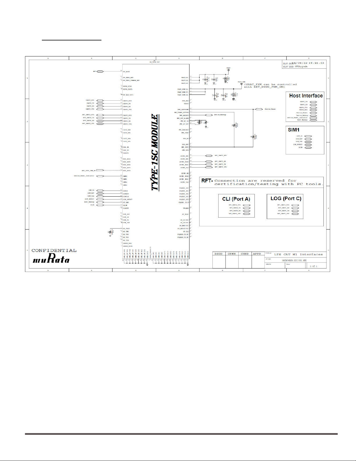
2.11 Reference Circuit ................................................................................................................................... 22
3 Power ....................................................................................................................................................................... 22
3.1 Power Up Sequence .............................................................................................................................. 22
3.2 Power Down Sequence .......................................................................................................................... 22
3.3 Power Supply Scenarios (by Battery Type) ............................................................................................ 22
LiPo Battery (3.2 ~ 4.35 V) ............................................................................................................. 23
CR17450 Battery (2.2 ~ 3.0 V) ....................................................................................................... 23
AA Lithium Battery (1.0 ~ 1.5 V) ..................................................................................................... 23
3.4 PMU ....................................................................................................................................................... 23
PMU_SHUTDOWN ........................................................................................................................ 24
PMU_POWER_BUTTON ............................................................................................................... 24
PMU_WAKEUP .............................................................................................................................. 24
4 SIM Interface ............................................................................................................................................................ 24
5 Host Interface ........................................................................................................................................................... 24
6 Antenna Requirements ............................................................................................................................................ 25
6.1 Main Antenna ......................................................................................................................................... 25
6.2 MIPI RFFE for Antenna Tuning .............................................................................................................. 26
6.3 GPS Coexistence ................................................................................................................................... 26
7 APPLICATION PCB DESIGN .................................................................................................................................. 26
7.1 Solder Reflow ......................................................................................................................................... 26
Antenna Installation Guidelines ...................................................................................................... 27
PCB Design Guidelines .................................................................................................................. 27
Transmission line design ................................................................................................................ 28
8 FCC Notice ............................................................................................................................................................... 29
8.1 FCC Test Data........................................................................................................................................ 29
8.2 ISED Test Data....................................................................................................................................... 29
Copyright © Murata Manufacturing Co., Ltd. All rights reserved. September 2018
Application Note: LBAD0XX1SC, v0.4 7/1/19 Page 3 of 29 www.murata.com
Page 4

LIST OF FIGURES
Figure 1 Module block diagram ........................................................................................................ 8
Figure 2 Land pattern: top view, in millimeters ................................................................................ 12
Figure 3 Pin layout: top view .......................................................................................................... 13
Figure 4 Power up sequence ......................................................................................................... 22
Copyright © Murata Manufacturing Co., Ltd. All rights reserved. September 2018
Application Note: LBAD0XX1SC, v0.4 7/1/19 Page 4 of 29 www.murata.com
Page 5

LIST OF TABLES
Table 1 Supported bands ................................................................................................................................................... 8
Table 2 Power supply range ............................................................................................................................................. 11
Table 3 Temperature range .............................................................................................................................................. 11
Table 4 Pin description ..................................................................................................................................................... 21
Table 5 I/Os with PU/PD ................................................................................................................................................... 21
Table 6 Special UART signals for certification/testing ..................................................................................................... 22
Table 7 PMU system signals ............................................................................................................................................ 23
Table 8 Host interface signals .......................................................................................................................................... 25
Copyright © Murata Manufacturing Co., Ltd. All rights reserved. September 2018
Application Note: LBAD0XX1SC, v0.4 7/1/19 Page 5 of 29 www.murata.com
Page 6

Acronym
Meaning
3GPP
3rd Generation Partnership Project
API
Application Programming Interface
CPU
Central Processing Unit
eDRX
Extended Discontinuous Reception
eMTC
enhanced Machine-Type Communication
EVB
Evaluation Board
FW
Firmware
GPIO
General Purpose Input/Output
FEM
Front End Module
HF
Hyper Frame (10.24s)
MIPI
Mobile Industry Processor Interface
IoT
Internet of Things
LiPo
Lithium-ion Polymer
LTE
Long Term Evolution
LPWA
Low Power Wide Area
PC
Personal Computer
PSM
Power Saving Mode
PTW
Paging Time Window
RF
Radio Frequency
RFFE
RF Front End
SoC
System on Chip
SW
Software
UART
Universal Asynchronous Receiver/Transmitter
USB
Universal Serial Bus
1 Introduction
1.1 Scope
This document introduces the Murata Type1SC LTE CatM1/NB1 module and presents some possible and
recommended guidelines for developing new products based on this module. The information given should be
used as a guide and a starting point for properly developing products with the Murata module.
1.2 Audience
This document is intended for Murata customers, especially system architects and HW engineers, to design
products based on the Murata Type1SC module.
1.3 Contact Information and Support
For general contact, technical support services, technical questions and report documentation errors contact
Murata Technical Support at techhelp@murata.com
Please keep us informed of your comments and suggestions for improvements. Murata will take into
consideration any and all feedback from the users of this information.
1.4 Text Conventions
Danger – This information MUST be followed or catastrophic equipment failure or bodily injury may occur.
Caution/Warning
Alerts the user to important points about using the product; if these points are not followed, the product
and end user equipment may fail or malfunction.
Tip/Information – Provides advice and suggestions that may be useful when using the product.
.
1.5 Acronyms
Copyright © Murata Manufacturing Co., Ltd. All rights reserved. September 2018
Application Note: LBAD0XX1SC, v0.4 7/1/19 Page 6 of 29 www.murata.com
Page 7
1.6 Related Documents
[1] Type1SC Reference Schematics
Copyright © Murata Manufacturing Co., Ltd. All rights reserved. September 2018
Application Note: LBAD0XX1SC, v0.4 7/1/19 Page 7 of 29 www.murata.com
Page 8
Product
LTE Bands
Regions
LBAD0XX1SC
LB: B5/B8/B12/B13/B14/B17/B18/B19/B20/B26/B28
MB: B1:B2/B3/B4/B25
Americas, EU and
2 Introduction
Type1SC is Murata’s new LTE series for IoT applications. The module can be used as a wireless communication
front-end for wearable products, offering mobile communication features to an external host CPU through its
interfaces.
Note: NB1 will be supported in a future firmware release.
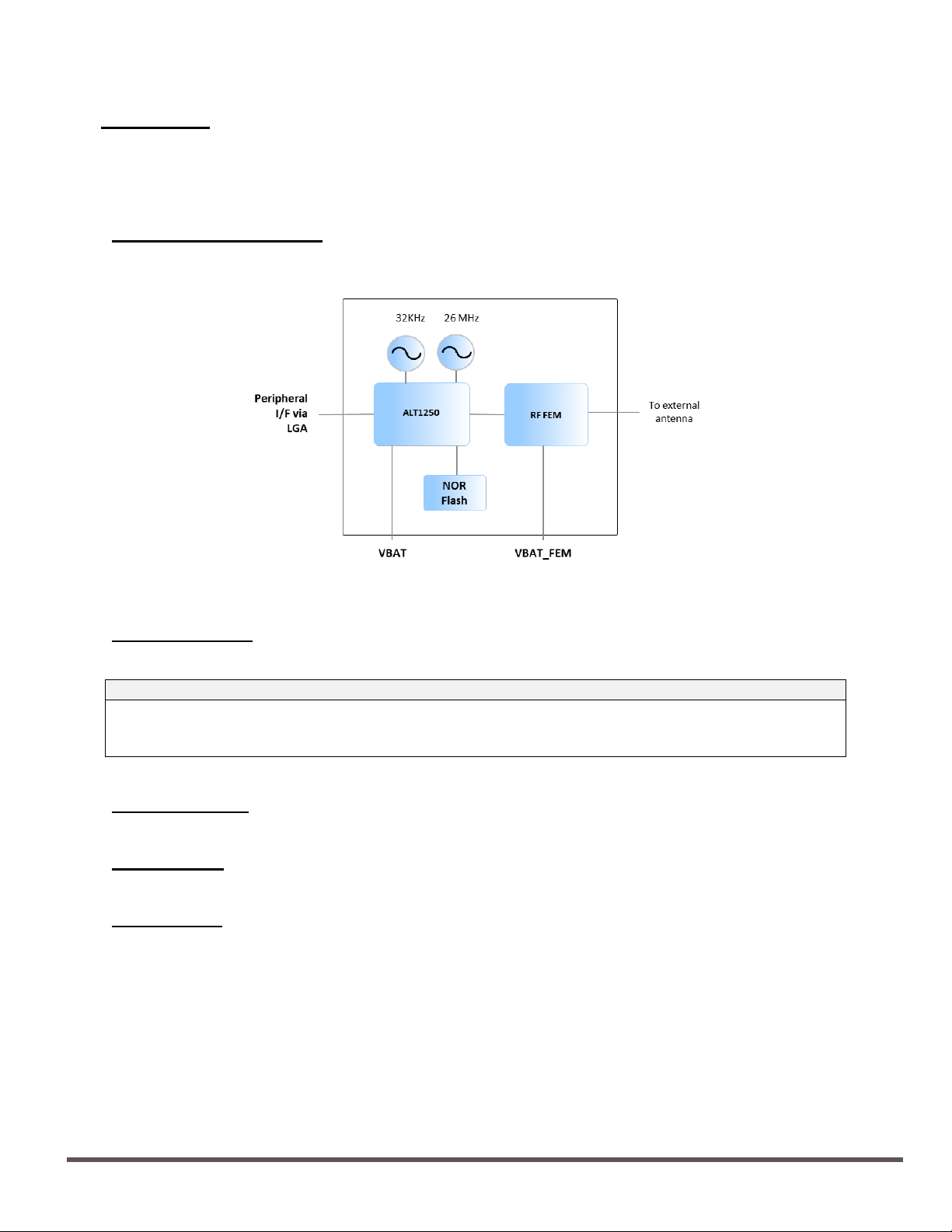
2.1 High Level Block Diagram
The following block diagram illustrates the module which contains the ALT1250 LTE Cat M1/NB1 SoC, RF FEM,
128 MBits flash and clocks.
Figure 1 Module block diagram
2.2 Supported bands
The module supports the following bands:
Table 1 Supported bands
ASEAN
2.3 Tx Output Power
The LTE bands in the 1SC module meet the 3GPP spec for a Power Class 3 device (23 dBm).
2.4 Rx Sensitivity
The receive sensitivity of the module will be around -103 dBm.
2.5 Power Modes
The 1SC module has the following power modes
• LS: Provides very fast entry and recovery time and is mainly used for very short sleeps. It is used for CDRX
mode during the networking process.
• DS: Provides fast recovery and entry time and is mainly used during the IDRX networking mode.
• DH2: Provides medium entry and recovery time and is mainly used during the EDRX and IDRX networking
modes.
• DH1: Same as DH2, however IO logic is not retained.
• DH05: Provides long entry and recovery times and is mainly used for very long inactivity intervals like PSM.
The IO output values are retained in this mode.
• DH0: Same as DH05, however IO output values are not retained.
Copyright © Murata Manufacturing Co., Ltd. All rights reserved. September 2018
Application Note: LBAD0XX1SC, v0.4 7/1/19 Page 8 of 29 www.murata.com
Page 9

The device chooses the described power modes according to the networking state and the maximum allowed chip
power mode configuration.
An application note will be provided to show how to configure the module and the R&S CMW500 to test the different
power modes.
LS Power Mode
Only one of the following pins can be used to wake up the device
• RTC Expiration
• PMU_POWER_BUTTON
• PMU_WAKEUP
• PMU_SHUTDOWN
• AntiTamper
Other digital interface pins can also be configured to wake up the system (up to 10 GPIO’s can be used). Serial
interface pins are not active in this mode
DS Power Mode
This mode is the same as LS, but requires lower power consumption due to the unused reference clock.
The average current draw in this mode of operation is 2.5mA.
DH0 Power Mode
The following occurs in the DH0 power mode:
• All digital logic is powered down
• Memories are not retained
• IO’s are not stored
• The RTC is on
• One of the following dedicated pins is used to wake from this mode:
o RTC Expiration
o PMU_POWER_BUTTON
o PMU_WAKEUP
o PMU_SHUTDOWN
o AntiTamper
The average current draw in this mode of operation is 1.7uA.
DH1 Power Mode This mode is similar to DH0, however it enables memory retention to store the system sate. A Wakeup event will only initiate a boot flow in a case of state full configuration
The average current draw in this mode of operation is 48uA.
DH2 Power Mode This mode is similar to DH1, however it also enables output IOs to latch and wakeup from digital inputs (up to 10 GPIO’s can be used)
The current draw is similar to DH1, but will depend on the extra current draw of the GPIOs.
PSM Current Draw Currently the PSM mode of operation is not optimized so the current draw will vary. This will be fixed in a future version of firmware. This figure below represents the worst-case condition (This was tested with RK _50). Current ideal conditions the average current should be 33.76mA.
Copyright © Murata Manufacturing Co., Ltd. All rights reserved. September 2018
Application Note: LBAD0XX1SC, v0.4 7/1/19 Page 9 of 29 www.murata.com
Page 10

eDRX Current Draw The SIM card will have a major impact on this feature. Network Carriers will support different modes of operation. The R&S test SIM for the CMW500 does not support SIM deactivation during eDRX cycles. This caused the number to be significantly greater than a setup with a deactivation mode. The feature below shows result using the CMW500 test SIM. Under good conditions using a SIM that can be deactivated, the current draw could be as low as 86uA instead of 377uA for this setup. This setup was using an eDRX cycle of 81.92 s (8 HF).
Copyright © Murata Manufacturing Co., Ltd. All rights reserved. September 2018
Application Note: LBAD0XX1SC, v0.4 7/1/19 Page 10 of 29 www.murata.com
Page 11

Parameter
Range
Absolute maximum rating
VBAT
-0.3 V – 4.35 V
VBAT_FEM
-0.5 V – 5.2 V
Operating voltage range
VBAT
2.2 V – 4.35 V
VBAT_FEM
3.2 V – 4.5 V
I/O (1.8V typ)
1.7 V – 1.9 V
VIO
VDDIO
1.7 V – 1.9 V
V
VDD
1.0 V – 1.1 V
Range
Note
Storage temperature range
-40 ºC – 85 ºC
Storage and non-operational
Operating temperature range
-40 ºC – 85 ºC
Module is fully functional
†
-20 ºC – 55 ºC
Module is fully functional† and
fully meets 3GPP specification
(†) Functional: the module is able to connect to PDN and transfer data.
2.6 Certification and Regulatory
The module is certified to GCF 3.70.2 and PTCRB 5.36. The module is fully compliant to CAT M1 3GPP release
13.
The module is FCC/IC certified (HSW-xxxxx) and RED ETSI EN 301908-13 compliant.
2.7 Power Supply Range
RETENTION
2.8 Temperature Range
Table 2 Power supply range
Table 3 Temperature range
Copyright © Murata Manufacturing Co., Ltd. All rights reserved. September 2018
Application Note: LBAD0XX1SC, v0.4 7/1/19 Page 11 of 29 www.murata.com
Page 12

2.9 Mechanical Specifications
• Dimensions: 11.1 × 11.4 × 1.4 mm
• Weight: 443 mg
3
(typ)
Figure 2 Land pattern: top view, in millimeters
Copyright © Murata Manufacturing Co., Ltd. All rights reserved. September 2018
Application Note: LBAD0XX1SC, v0.4 7/1/19 Page 12 of 29 www.murata.com
Page 13

2.10 Pin Layout and Descriptions
1SC
Module Pin Name
ALT12
ALT1250 IC Symbol Pin
Type
Input/
Reset
IO
Description
1
DEBUG_RSTN
P4
DEBUG_RSTN
Digital
I/O
PU
VDDIO
Reserved (No Connection)
2
DEBUG_SEL
M4
DEBUG_SEL/
GPIO31
Digital
I/O
PD
VDDIO
Reserved (No Connection)
3
EJ_TDO
N5
EJ_TDO/
Digital
I/O
PU
VDDIO
Reserved (No Connection)
4
EJ_TRST
J5
EJ_TRST/
Digital
I/O
PD
VDDIO
Reserved (No Connection)
5
PMU_AT_IN
R3
PMU_AT_IN
Analog
I VRTC
Anti-tamper input; short to GND
6
PMU_WAKEUP
P2
PMU_WAKEUP
Analog
I VRTC
Device Wakeup active high;
7
VDD_RF
L1
PMU_VO_RF
Power
O
MIPI RFFE VIO (antenna tuning)
8
VSIM
R1
PMU_VO_SIM
Power
O
SIM LDO output
9
VDD_AUX
T2
PMU_VO_AUX_LDO
Power
O
SC2 LDO output
10
VDD_XO
N1
PMU_VO_XO
Power
O
Reserved (No Connection)
11
SIMIO
M10
SC_IO/
Digital
I/O
PD
VDDIO
SIM Data 1.8V
Pin
No
50 IC
Pin No
Name
GPIO22
GPIO20
GPIO14
Figure 3 Pin layout: top view
Output
Value
Domain/
Supply
if not used
Device Wake-Up
Copyright © Murata Manufacturing Co., Ltd. All rights reserved. September 2018
Application Note: LBAD0XX1SC, v0.4 7/1/19 Page 13 of 29 www.murata.com
Page 14

1SC
Module Pin Name
ALT12
ALT1250 IC Symbol Pin
Type
Input/
Reset
IO
Description
12
I2C1_SDA
H2
I2C1_SDA/
GPIO44
Digital
I/O
PU
VDDIO
Reserved (No Connection)
13
I2C1_SCL
H4
I2C1_SCL/
GPIO45
Digital
I/O
PU
VDDIO
Reserved (No Connection)
14
I2C0_SCL
L7
I2C0_SCL/
GPIO43
Digital
I/O
PU
VDDIO
Reserved (No Connection)
15
I2C0_SDA
J7
I2C0_SDA/
GPIO42
Digital
I/O
PU
VDDIO
Reserved (No Connection)
16
VBAT_FEM
Power
I
Input from battery to FEM
17
VBAT_FEM
Power
I
Input from battery to FEM
18
VBAT_FEM
Power
I
Input from battery to FEM
19
GND
20
UART2_RX
H14
UART2_RX/
GPIO27
Digital
I/O
PU
VDDIO
• Default is UART1 Receive
21
UART2_CTS
G15
UART2_CTS/
GPIO29
Digital
I/O
PD
VDDIO
• Default is UART1 Clear to
Pin
No
50 IC
Pin No
Name
SPIS_MRDY/
PWM 3/
MCU_I2C1_SDA/
MCU_FLA SH1_SCK/
UART0_RI/
MCU_S PIM1_CLK_A/
MCU_PWM3/
SPIS_CLK/
LED3/
M CU_I2C1_SCL/
MCU_FLASH1_ CS_N/
UART0_DTR/
MCU_SPI M1_EN0_A/
MCU_LED3/
SPIS_MISO/
KEYPA D9/
FEM19/
MCU_I2C0_SCL/
UART0_DSR/
SPIS_MOSI/
CLKO UT/
KEYPAD7/
MCU_I2C0_SD A/
UART0_DCD/
MCU_CLKOU T/
Output
Value
Domain/
Supply
Copyright © Murata Manufacturing Co., Ltd. All rights reserved. September 2018
Application Note: LBAD0XX1SC, v0.4 7/1/19 Page 14 of 29 www.murata.com
SPIS_MOSI_A/
P WM2/
EJ1_TDI_B/
UART1_RX/
MCU_UART1_RX/
MCU_SPIM1_MISO_A/
MCU_SPIM0_MISO_A/
UART3_RX_B/
MCU_PWM2/
SPIS_MRDY_A/
E J1_TRST_B/
UART1_CTS/
MCU_UART1_CTS/
MCU_SPIM1_CLK_A/
MCU_SPIM0_CLK_A/
U ART3_CTS_B/
Data
• Dedicated for debug
interface
Send
• Dedicated for debug
interface
Page 15

1SC
Module Pin Name
ALT12
ALT1250 IC Symbol Pin
Type
Input/
Reset
IO
Description
22
UART2_TX
G13
UART2_TX/
GPIO28
Digital
I/O
PU
VDDIO
• Default is UART1 Transmit
23
GND
24
RF_GNSS_COMM
RF O GNSS receiver output
25
RF_GNSS_ANT
RF I GNSS receiver input
26
GND 27
RF_AUX_OUT1
RF Reserved (No Connection)
28
GND 29
RF_RXTX
RF LTE RF in/out signal
30
GND
31
PWM3
N13
PWM3/
GPIO53
Digital
I/O
PU
VDDIO
TX Indicator
32
PWM0
P10
PWM0/
GPIO50
Digital
I/O
PD
VDDIO
Device reset status (HI)
33
AUX_ADC4
H12
AUX_ADC4/
GPIO5
Digital
I/O
PD
VDDIO
External DCDC control
34
AUX_ADC3
J13
AUX_ADC3/
GPIO4
Digital
I/O
PU
VDDIO
Reserved (No Connection)
35
AUX_ADC2
K14
AUX_ADC2/
GPIO3
Digital
I/O
PU
VDDIO
Reserved (No Connection)
Pin
No
ON_ANT
50 IC
Pin No
Name
SPIS_MISO_A/
FE M22/
EJ1_TMS_B/
UART1_TX/
MCU_UART1_TX/
MCU_SPIM1_MOSI_A/
MCU_SPIM0_MOSI_A/
UART3_TX_B/
I2C1_SDA/
SC_SWP/
F EM29/
MCU_CC_OUT3/
MCU_CC_IN3/
MCU_LED3/
MCU_P WM3/
Output
Value
Domain/
Supply
Data
• Dedicated for debug
interface
CLKOUT/
MCU_CC_O UT0/
MCU_CC_IN0/
MCU_CLK OUT/
FEM28/
MCU_PWM0/
FEM7/
PCM_OUT/
MCU_LED0/
MCU_CC_OUT1/
FEM6/
PCM_IN/
K EYPAD4/
MCU_SPIM1_CLK_B/
MCU_I2C1_SCL/
SWDAT/
MCU_CC_IN3/
FEM5/
PCM_FS/
K EYPAD7/
MCU_SPIM1_EN0_B/
MCU_I2C1_SDA/
SWCLK/
MCU_CC_IN2/
(DCDC_EN)
Copyright © Murata Manufacturing Co., Ltd. All rights reserved. September 2018
Application Note: LBAD0XX1SC, v0.4 7/1/19 Page 15 of 29 www.murata.com
Page 16

1SC
Module Pin Name
ALT12
ALT1250 IC Symbol Pin
Type
Input/
Reset
IO
Description
36
AUX_ADC0
L13
AUX_ADC0/
GPIO1
Digital
I/O
PU
VDDIO
Reserved (No Connection)
37
AUX_ADC1
M14
AUX_ADC1/
GPIO2
Digital
I/O
PD
VDDIO
GNSS coexistence indicator
38
GND
39
SF_SO/IO1
Y14
FLASH0_IO1/
Digital
I/O
PD
V_FLASH
Reserved (No Connection)
40
SF_SI/IO0
AA15
FLASH0_IO0/
Digital
I/O
PU
V_FLASH
Reserved (No Connection)
41
SF_nHOLD/IO3
Y12
FLASH0_IO3/
Digital
I/O
PU
V_FLASH
Reserved (No Connection)
42
SF_nWP/IO2
AA13
FLASH0_IO2/
Digital
I/O
PD
V_FLASH
Reserved (No Connection)
43
SPIM0_EN0
P12
SPIM0_EN0/
GPIO35
Digital
I/O
PU
VDDIO
Port C: UART RTS
44
SPIM0_EN1
R13
SPIM0_EN1/
GPIO36
Digital
I/O
PU
VDDIO
External LNA GNSS
45
SPIM0_MISO
T12
SPIM0_MISO/
GPIO34
Digital
I/O
PU
VDDIO
Port C: UART RX
46
SPIM0_MOSI
U13
SPIM0_MOSI/
/GPIO33
Digital
I/O
PU
VDDIO
Port C: UART TX
47
NC
Reserved (No Connection)
Pin
No
50 IC
Pin No
Name
I2C1_SCL/
MCU_ CC_IN0/
KEYPAD9/
MCU_LED 4/
PWM2/
MCU_PWM2/
FEM4/
PCM_CLK/
KEYPAD6/
CLKOUT/
MCU_LED 1/
MCU_CLKOUT/
MCU_CC_I N1/
GPIO71
GPIO70
GPIO73
Output
Value
Domain/
Supply
GPIO72
UART1_RTS/
MC U_PCM_OUT_A/
UART0_DSR/
MCU_SPIS_CLK_B/
SWDAT/
MCU_SPIM0_EN0_A/
SPIS_SRDY_ABC/
KEYPAD4/
FEM18/
MCU_SPIS_SRDY_AB/
MCU_CC_IN2/
MCU_FLASH1_CS_N1/
MCU_CC_ OUT2/
UART1_RX/
MC U_PCM_FS_A/
UART0_DTR/
MCU_SPIS_MOSI_B/
MCU_U ART1_RX/
MCU_SPIM0_MISO
_AB/
UART1_TX/
MC U_PCM_IN_A/
UART0_DCD/
MCU_SPIS_MISO_B/
SWCLK/
MCU_SPIM0_MOSI_AB
Copyright © Murata Manufacturing Co., Ltd. All rights reserved. September 2018
Application Note: LBAD0XX1SC, v0.4 7/1/19 Page 16 of 29 www.murata.com
Page 17

1SC
Module Pin Name
ALT12
ALT1250 IC Symbol Pin
Type
Input/
Reset
IO
Description
48
VFLASH
AA5
PMU_VO_FLASH
Power
O
Reserved (No Connection)
49
VDDIO
Y6
PMU_VO_IO
Power
O
IO reference
50
VDD_RET
V8
PMU_VO_RET
Power
O
Debug monitoring only
51
FLASH0_CS_N1
V14
FLASH0_CS_N1/
GPIO66
Digital
I/O
PU
V_FLASH
GNSS SFN indication
52
FLASH1_CS_N
M6
MCU_FLASH1_CS_N/
GPIO54
Digital
I/O
PU
VDDIO
Reserved (No Connection)
53
FLASH1_IO1
R7
MCU_FLASH1_IO1/
GPIO57
Digital
I/O
PU
VDDIO
Reserved (No Connection)
54
FLASH0_CS_N2
W11
FLASH0_CS_N2/
GPIO78
Digital
I/O
PU
V_FLASH
Reserved (No Connection)
55
FLASH1_SCK
U7
MCU_FLASH1_SCK/
GPIO55
Digital
I/O
PD
VDDIO
Reserved (No Connection)
56
PMU_VBACKUP
W7
PMU_VBACKUP
Power
I
Input from backup battery or NC
57
PMU_VRTC
W5
PMU_VRTC
Power
O
Use for PMU_SHUTDOWN and
58
VBAT
U3
PMU_VBAT_LDO
Power
I
Voltage from Battery
59
V2
PMU_VBAT_DCDC_V2
Power
I
60
W1
PMU_VBAT_DCDC_W1
Power
I
61
EJ_TDI
L5
EJ_TDI/
Digital
I/O
PD
VDDIO
Reserved (No Connection)
62
EJ_TMS
K4
EJ_TMS/
GPIO19
Digital
I/O
PD
VDDIO
Reserved (No Connection)
63
PMU_AT_OUT
N3
PMU_AT_OUT
Analog
O VRTC
Anti-tamper output; connect to
64
PMU_SHUTDOWN
M2
PMU_SHUTDOWN
Analog
I
PU
VRTC
Shutdown active low
65
PMU_EXT_ALARM
L3
PMU_EXT_ALARM/
GPO0
Analog
O VDDIO
Debug monitoring only
66
PMU_POWER_BUT
K2
PMU_POWER_BUTTO
Analog
I
PU
VRTC
Power button active low
67
PMU_ATB
J3
PMU_ATB
Test
I/O VBAT
Reserved (No Connection)
Pin
No
50 IC
Pin No
Name
FEM24/
PWM0/
KEYPAD5/
LED0/
MCU_LED0/
FLASH1_CS_N1/
MCU_PWM0/
I2C0_SCL/
UART0_TX/
KEYPAD1/
MCU_ I2C0_SCL/
MCU_CC_OUT1/
M CU_UART1_TX/
FEM27/
LED5/
MCU_LED5/
Output
Value
Domain/
Supply
PWM1/
K EYPAD8/
LED1/
MCU_LED1/
M CU_PWM1/
GPIO21
SWDAT/
ALARM/
3 2KHZ_CLK_OUT/
if not used
PMU_POWER_BUTTON pull
source
PMU_AT_IN or NC if not used
TON
Copyright © Murata Manufacturing Co., Ltd. All rights reserved. September 2018
Application Note: LBAD0XX1SC, v0.4 7/1/19 Page 17 of 29 www.murata.com
N
Page 18

1SC
Module Pin Name
ALT12
ALT1250 IC Symbol Pin
Type
Input/
Reset
IO
Description
68
SIMRST
M8
SC_RST/
Digital
I/O
PD
VDDIO
SIM Reset 1.8V
69
SIMCLK
L9
SC_CLK/
GPIO15
Digital
I/O
PD
VDDIO
SIM Clock 1.8V
70
SIM_DETECT
J11
SC_DET/
GPIO16
Digital
I/O
PD
VDDIO
SIM Detection 1.8V
71
SC_SWP
J9
SC_SWP/
GPIO17
Digital
I/O
PD
VDDIO
Host Wake-Up Active HI
72
UART0_RTS
K8
UART0_RTS/
GPIO26
Digital
I/O
PU
VDDIO
• Default is UART0 Request
73
UART0_TX
K10
UART0_TX/
GPIO24
Digital
I/O
PU
VDDIO
• Default is UART0 Transmit
74
UART2_RTS
K6
UART2_RTS/
GPIO30
Digital
I/O
PU
VDDIO
• Default is UART1 Request
75
UART0_RX
G11
UART0_RX/
GPIO23
Digital
I/O
PU
VDDIO
• Default is UART0 Receive
76
UART0_CTS
G9
UART0_CTS/
GPIO25
Digital
I/O
PU
VDDIO
• Default is UART0 Clear to
77
RFFE_SCLK
H6
RFFE_SCLK/
GPIO11
Digital
I/O
PD
VDDIO
MIPI RFFE Clock (antenna
Pin
No
50 IC
Pin No
Name
GPIO13
PWM0/
FEM12/
MCU_PWM0/
CLKOUT/
FEM13/
P WM3/
MCU_PWM3/
EJ1_TDO_AB/
CLK32KHZ_EXT/
MCU_CLKOUT/
MCU_CC_OUT3/
SPIM0_EN0_A/
I2C0_SDA/
UART2_RTS/
MCU_ UART0_RTS/
EJ1_TCK_A/
MC U_I2C0_SDA/
MCU_SPIM0_EN0_B/
UART3_RTS_A/
Output
Value
Domain/
Supply
to Send
• Data host interface; UART
RTS (HI)
SPIM0_MOSI_A/
FEM15/
UART2_TX/
MCU_UAR T0_TX/
EJ1_TMS_A/
UART3_T X_A/
SPIS_CLK_A/
FE M23/
EJ1_TCK_B/
UART1_RTS/
MCU_UART1_RTS/
MCU_SPI M1_EN_A/
MCU_SPIM0_EN0_A/
UART3_RTS_B/
SPIM0_MISO_A/
FEM14/
UART2_RX/
MCU_UA RT0_RX/
EJ1_TDI_A/
UART3_ RX_A/
SPIM0_CLK_A/
I2 C0_SCL/
UART2_CTS/
MCU_U ART0_CTS/
EJ1_TRST_A/
MCU_I2C0_SCL/
MCU_SPIM0_CLK_B/
UART3_CTS_A/
Data
• Data host interface; UART
TX (HI)
to Send
• Dedicated for debug
interface
Data
• Data host interface; UART
RX (HI)
Send
• Data host interface; UART
CTS (HI)
Copyright © Murata Manufacturing Co., Ltd. All rights reserved. September 2018
Application Note: LBAD0XX1SC, v0.4 7/1/19 Page 18 of 29 www.murata.com
FEM10/
tuning)
Page 19

1SC
Module Pin Name
ALT12
ALT1250 IC Symbol Pin
Type
Input/
Reset
IO
Description
78
RFFE_SDATA
H8
RFFE_SDATA/
GPIO12
Digital
I/O
PD
VDDIO
MIPI RFFE data (antenna
79
GND
Ground
80
GND
Ground
81
GND
Ground
82
PWM1
L11
PWM1/
GPIO51
Digital
I/O
PU
VDDIO
Reserved (No Connection)
83
PWM2
M12
PWM2/
GPIO52
Digital
I/O
PU
VDDIO
Reserved (No Connection)
84
SPIM1_MISO
N9
MCU_SPIM1_MISO/
GPIO39
Digital
I/O
PD
VDDIO
SC2_IO
85
SPIM1_EN
P8
MCU_SPIM1_EN/
GPIO40
Digital
I/O
PU
VDDIO
SC2_DET
86
SPIM1_MOSI
T8
MCU_SPIM1_MOSI/
GPIO38
Digital
I/O
PD
VDDIO
SC2_CLK
87
SPIM1_CLK
R9
MCU_SPIM1_CLK/
GPIO41
Digital
I/O
PD
VDDIO
SC2_RST
88
SF_CLK
W15
FLASH0_SCK/
GPIO67
Digital
I/O
PD
V_FLASH
Reserved (No Connection)
89
GND
90
USB_DN
J15
USB_DN/
GPI64_3V3
Digital
I USB_V3P
3
Reserved (No Connection)
Pin
No
50 IC
Pin No
Name
FEM11/
I2C0_SDA/
MCU_SPI
M1_MISO_AB/
KEYPAD5/
MC U_CC_OUT1/
MCU_CC_IN1/
MCU_PWM1/
I2C0_SCL/
MCU_SPIM1_MOSI_AB
/
FEM16/
MCU_C C_OUT2/
MCU_CC_IN2/
MCU_PWM2/
Output
Value
Domain/
Supply
tuning)
SPIS_M OSI_A/
KEYPAD6/
PWM1/
MCU_SPIS_MOSI_A/
SC_IO/
MCU_PCM_FS_B/
MCU_PWM1/
SPIS_CLK_A/
KEYPAD8/
PWM3/
MCU_SPIS_CLK_A/
SC_DET/
MCU_PCM_ IN_B/
MCU_PWM3/
SPIS_MI SO_A/
PWM2/
MCU_PWM2/
MCU_SPIS_MISO_A/
SC_CLK/
MCU_PCM_OUT_B/
SPIS_MRD Y_A/
PWM0/
MCU_CC_OUT0/
MCU_SPIS_MRDY_A/
SC_RST/
MCU_PCM_CLK_B/
Copyright © Murata Manufacturing Co., Ltd. All rights reserved. September 2018
Application Note: LBAD0XX1SC, v0.4 7/1/19 Page 19 of 29 www.murata.com
Page 20

1SC
Module Pin Name
ALT12
ALT1250 IC Symbol Pin
Type
Input/
Reset
IO
Description
91
USB_DP
L15
USB_DP/
GPI63_3V3
Digital
I/O USB_V3P
3
Reserved (No Connection)
92
GND
93
USB3V3
N15
USB_V3P3
Digital
I VDDIO
Reserved (No Connection)
94
SPIM0_CLK
V12
SPIM0_CLK/
GPIO37
Digital
I/O
PU
VDDIO
Port C: UART CTS
95
PCM_FS
R11
PCM_FS/
GPIO47
Digital
I/O
PU
VDDIO
Reserved (No Connection)
96
PCM_IN
N11
PCM_IN/
GPIO48
Digital
I/O
PU
VDDIO
Reserved (No Connection)
97
PCM_OUT
T10
PCM_OUT/
GPIO49
Digital
I/O
PU
VDDIO
Reserved (No Connection)
98
PCM_CLK
V10
PCM_CLK/
GPIO46
Digital
I/O
PD
VDDIO
Reserved (No Connection)
99
GND
100
CLKOUT
U9
CLKOUT/
GPIO60
Digital
O
PD
VDDIO
Reserved (No Connection)
101
GND
102
PMU_VCAP
V6
PMU_VCAP
Analog
O VBAT
Connecting external capacitor as
used
Pin
No
50 IC
Pin No
Name
UART1_CTS/
MC U_PCM_CLK_A/
UART0_RI/
MCU_SPIS_MRDY_B/
MCU_UA RT1_TX/
MCU_SPIM0_CLK_A/
UART1_RTS/
KEYPA D1/
FEM21/
MCU_FLASH1_IO 1/
MCU_LED5/
MCU_UART1_ RTS/
MCU_PCM_FS/
UART1_RX/
KEYPAD 2/
LED4/
MCU_FLASH1_IO2/
MCU_LED4/
MCU_UART1_RX/
MCU_PCM_IN/
Output
Value
Domain/
Supply
UART1_TX/
KEYPA D3/
PWM2/
MCU_FLASH1_IO 3/
MCU_PWM2/
MCU_UART1_TX/
MCU_PCM_OUT/
UART1_CTS/
KEYP AD0/
FEM20/
MCU_FLASH1_I O0/
MCU_LED2/
MCU_UART1_CTS/
MCU_PCM_CLK/
32KHZ_CLK_OUT/
PWM0/
FLASH1_CS_N1/
LED2/
MCU_CLKOUT/
MCU_CC_OU
T1/
MCU_PWM0/
Copyright © Murata Manufacturing Co., Ltd. All rights reserved. September 2018
Application Note: LBAD0XX1SC, v0.4 7/1/19 Page 20 of 29 www.murata.com
backup for VBAT or NC if not
Page 21

1SC
Module Pin Name
ALT12
ALT1250 IC Symbol Pin
Type
Input/
Reset
IO
Description
103
FLASH1_IO3
N7
MCU_FLASH1_IO3/
GPIO59
Digital
I/O
PU
VDDIO
Reserved (No Connection)
104
FLASH1_IO2
P6
MCU_FLASH1_IO2/
GPIO58
Digital
I/O
PD
VDDIO
Reserved (No Connection)
105
FLASH1_IO0
T6
MCU_FLASH1_IO0/
GPIO56
Digital
I/O
PU
VDDIO
Reserved (No Connection)
106
EJ_TCK
R5
EJ_TCK/
GPIO18
Digital
I/O
PD
VDDIO
Reserved (No Connection)
107-
GND_PAD
1SC Pin No
Module Pin Name
PD (KΩ)
PU (KΩ)
PU Source
Description
4
EJ_TRST
10
Reserved (No Connection)
5
PMU_AT_IN
Short to GND
Anti-tamper input; short to GND if not used
64
PMU_SHUTDOWN
560
VRTC
Shutdown active low; PU to PMU_VRTC
66
PMU_POWER_BUTTON
560
VRTC
Power button active low; PU to PMU_VRTC
Pin
No
115
50 IC
Pin No
Name
I2C1_SCL/
UART0_RTS/
KEYPAD3/
MCU_I2C1_SCL/
MCU_CC_OUT3/
MCU_UART1_RTS/
I2C1_SDA/
UART0_CTS/
KEYPAD2/
MCU_I2C1_SDA/
MCU_CC_OUT2/
MCU_UART1_CTS/
I2C0_SDA/
UART0_RX/
KEYPAD0/
MCU_ I2C0_SDA/
MCU_CC_OUT0/
MCU_UART1_RX/
SWCLK/
Output
Value
Domain/
Supply
Table 4 Pin description
If not used, all pins except the following should be left disconnected.
Table 5 I/Os with PU/PD
The PMU_VRTC pin must not be used by any external component other than pull-ups for the
PMU_SHUTDOWN and PMU_POWER_BUTTON pins. It is prohibited to use the PMU_VRTC pin for any
other purpose.
The UARTs Port A (20, 21, 22, 74) and Port C (43, 45, 46, 94) signals should be brought out for control and
logging during certification/testing with PC tools.
Copyright © Murata Manufacturing Co., Ltd. All rights reserved. September 2018
Application Note: LBAD0XX1SC, v0.4 7/1/19 Page 21 of 29 www.murata.com
Page 22

1SC Pin No
Module Pin Name
Port
Signal
20
UART2_RX
A
UART RX
21
UART2_CTS
A
UART CTS
22
UART2_TX
A
UART TX
74
UART2_RTS
A
UART RTS
43
SPIM0_EN0
C
UART RTS
45
SPIM0_MISO
C
UART RX
46
SPIM0_MOSI
C
UART TX
94
SPIM0_CLK
C
UART CTS
Table 6 Special UART signals for certification/testing
2.11 Reference Circuit
A reference circuit for the Type1SC is provided in [1].
3 Power
Type1SC requires two power supplies, one for the LTE modem (VBAT) and the other for the RF FEM (VBAT_FEM).
The power supply must be capable of peak current output of at least 400mA and 800mA, respectively, for
VBAT and VBAT_FEM.
3.1 Power Up Sequence
The power up sequence is shown below. Type1SC will power up automatically once VBAT is connected to the
power supply.
3.2 Power Down Sequence
The supply to VBAT and VBAT_FEM should be turned off at the same time.
3.3 Power Supply Scenarios (by Battery Type)
A typical Type1SC based design uses a battery supply. The following are some possible battery supply scenarios:
• LiPo Battery (3.2 ~ 4.35 V)
• CR17450 Battery (2.2 ~ 3.0 V)
• AA Lithium Battery (1.0 ~ 1.5 V)
Copyright © Murata Manufacturing Co., Ltd. All rights reserved. September 2018
Application Note: LBAD0XX1SC, v0.4 7/1/19 Page 22 of 29 www.murata.com
Figure 4 Power up sequence
Page 23

Signal
Functionality
Input/
Polarity
PMU_SHUTDOWN
HW Reset
Input
Active Low
PMU_POWER_BUTTON
Reserved
Input
Active High
PMU_WAKEUP
Wakeup
Input
Active High
LiPo Battery (3.2 ~ 4.35 V)
The battery can supply the entire system (ALT1250 + FEM), without additional external power conditioning circuits.
CR17450 Battery (2.2 ~ 3.0 V) The ALT1250 can be fully functional without additional external power conditioning circuits. However, the FEM requires a higher voltage supply, so an external boost circuit is required to supply VBAT_FEM.
Boost converter such as TPS61021A may be turned on/off by the DCDC enable signal, AUX_ADC4 (pin
33, active high).
AA Lithium Battery (1.0 ~ 1.5 V) For battery range of 1.0 – 1.5 V, both ALT1250 and FEM require an additional boost circuit.
VBAT: ultra low I
synchronous boost converter such as TPS61098x may be used
Q
VBAT_FEM: boost converter such as TPS61021A may be turned on/off by the DCDC enable signal,
AUX_ADC4 (pin 33, active high).
3.4 PMU
ALT1250 includes integrated PMU which supplies current for all ALT1250 blocks, IOs, Flash, TCXO and UICC.
Output
Application Note: LBAD0XX1SC, v0.4 7/1/19 Page 23 of 29 www.murata.com
Copyright © Murata Manufacturing Co., Ltd. All rights reserved. September 2018
Table 7 PMU system signals
Page 24

PMU_SHUTDOWN This pin has the highest priority compared to other chip functionalities, therefore asserting it will always force a hard reset
3.4.1.1 External circuitry on PMU_SHUTDOWN
There are three use cases for PMU_SHUTDOWN pin connection:
1. Controlled by external host.
2. Controlled by mechanical switch.
3. Not used.
3.4.1.2 PMU_SHUTDOWN connected to external host
In this use case it is the responsibility of the host to drive this pin with proper voltage at all times (1.8V/0V).
In case of internal pull at the host IO, it is recommended to disable it when driving this pin to GND.
LTE CAT-M1/NB1 ALT1250 Based Chipset Power
Altair Semiconductor Proprietary and Confidential 45
3.4.1.3 PMU_SHUTDOWN connected to mechanical switch
In this case, when button is not pushed, the pin can be pulled up either by external 1.8V source or by PMU_VRTC.
If current during the time when button is pushed is a concern then some pullup disconnection circuitry should be
externally triggered when PMU_SHUTDOWN pin is being directed to GND
3.4.1.4 PMU_SHUTDOWN is not used
In this case PMU_SHUTDOWN pin should be tied directly to PMU_VRTC
This pin requires an external PU resistor, please see Table 5 more information.
The host connected to this pin should always keep the state of this pin (high/low) at a known state (not
floating) according to the required functionality.
PMU_POWER_BUTTON
This pin requires an external PU resistor, please see Table 5 more information.
The host connected to this pin should always keep the state of this pin (high/low) at a known state (not
floating) according to the required functionality.
PMU_WAKEUP This pin wakes-up the system from low power state.
4 SIM Interface
Since all digital IOs in Type1SC are in 1.8V domain, the module will support 1.8V SIM cards (Class-C).
For 3.0V SIM card support, an external voltage translator will be required.
5 Host Interface
Type1SC uses the following signals for the host interface. The UART interface is necessary for communication
between the host and Type1SC.
The device reset status signal can be used by the host to detect that the modem has completed a reset so
that the host can properly reset its internal state.
Copyright © Murata Manufacturing Co., Ltd. All rights reserved. September 2018
Application Note: LBAD0XX1SC, v0.4 7/1/19 Page 24 of 29 www.murata.com
Page 25

1SC Pin No
Module Pin Name
Direction
Description
Note
6
PMU_WAKEUP
HD
Device Wake-Up
Only needed if low power
32
PWM0
DH
Device reset status
64
PMU_SHUTDOWN
HD
Modem reset (active low)
Optional
71
SC_SWP
DH
Host Wake-Up
Only needed if low power
mode is required
72
UART0_RTS
DH
UART RTS
73
UART0_TX
DH
UART TX
75
UART0_RX
HD
UART RX
76
UART0_CTS
HD
UART CTS
Item
Value
Frequency range
Depending by frequency band(s) provided by
the most suitable antenna for that/those
band(s)
Bandwidth
LTE
Tx Band
(MHz)
Rx Band
(MHz)
Min
Max
Min
Max
B1
1920
1980
2110
2170
B2
1850
1910
1930
1990
B3
1710
1785
1805
1880
B4
1710
1755
2110
2155
B5
824
849
869
894
B8
880
915
925
960
B12
699
716
729
746
B13
777
787
746
756
B14
788
798
758
768
B17
704
716
734
746
B18
815
830
860
875
B19
830
845
875
890
B20
832
862
791
821
B25
1850
1915
1930
1995
B26
814
849
859
894
B28
703
748
758
803
mode is required
Table 8 Host interface signals
6 Antenna Requirements
The module has been FCC/IC/ETSI certified. However, since this is a module that does not have an RF
connector, an FCC Class 2 Permissive Change will be required to add the antenna to the grant.
6.1 Main Antenna
The antenna connection and board layout design are the most important aspect in the full product design as they
strongly affect the product overall performances, hence read carefully and follow the requirements and the
guidelines for a proper design. The antenna and antenna transmission line on PCB for a Type 1SC device shall
fulfill the following requirements:
the network operator, the customer shall use
Band
Copyright © Murata Manufacturing Co., Ltd. All rights reserved. September 2018
Application Note: LBAD0XX1SC, v0.4 7/1/19 Page 25 of 29 www.murata.com
Page 26

Impedance
50 ohm
Input power
> 23dBm Average power
VSWR absolute max
≤ 10:1 (limit to avoid permanent damage)
VSWR recommended
≤ 2:1 (limit to fulfill all regulatory
requirements)
Maximum permitted antenna gain including cable loss should be determined from Tables 8.1 and 8.2. Failure to
follow these guidelines wil result in radiated RF levels that exceed FCC MPE limits.
6.2 MIPI RFFE for Antenna Tuning
MIPI RFFE, is a dedicated control interface for the RF front-end subsystem. This interface allows antenna
designer to optimize antenna performance for different LTE bands. They can tune the antenna for different bands
by using a compliant MIPI RFFE switch. Currently the module only supports the Sony Switch (CXA4472GC-E).
The following signals are used for the MIPI interface.
RFFE_SCLK, RFFE_SDATA, RFFE_VDDIO_OUT
6.3 GPS Coexistence
Two pins are provided for GPS coexistence. AUX_ADC1 is used for GNSS coexistence indicator and
FLASH0_CS_N1 is used for GNSS SFN indication.
Other advanced GPS coexistence features will be available in a future firmware release.
7 APPLICATION PCB DESIGN
The Type 1SC modules have been designed to be compliant with a standard lead-free SMT process.
7.1 Solder Reflow
Recommended solder reflow profile:
Copyright © Murata Manufacturing Co., Ltd. All rights reserved. September 2018
Application Note: LBAD0XX1SC, v0.4 7/1/19 Page 26 of 29 www.murata.com
Page 27

Profile Feature
Pb-Free Assembly
Average ramp-up rate (TL to TP)
TBD
Preheat
– Time (min to max) (ts)
TBD
Tsmax to TL
– Ramp-up Rate
TBD
Time maintained above:
– Time (tL)
TBD
Peak Temperature (Tp)
TBD
Time within 5°C of actual Peak
Temperature (tp)
TBD
Ramp-down Rate
TBD.
Time 25°C to Peak
Temperature
TBD
Item
Value
Characteristic Impedance
50 ohm
Max Attenuation
0.3 dB
Coupling
Coupling with other signals shall be
avoided
Ground Plane
Cold End (Ground Plane) of antenna
ground pins
– Temperature Min (Tsmin)
– Temperature Max (Tsmax)
– Temperature (TL)
TBD
TBD
TBD
Antenna Installation Guidelines
• Install the antenna in a place covered by the LTE signal.
• If the device antenna is located farther than 20cm from the human body and there are no co-located
transmitter then the Murata FCC/IC approvals can be re-used by the end product.
• If the device antenna is located closer than 20cm from the human body or there are co-located transmitter
then the additional FCC/IC testing may be required for the end product (Murata FCC/IC approvals cannot
be reused).
• Antenna shall not be installed inside metal cases.
• Antenna shall be installed also according to antenna manufacturer instructions.
PCB Design Guidelines
When using the Type 1SC, since there's no antenna connector on the module, the antenna must be connected to
the Type 1SC antenna pad by means of a transmission line implemented on the PCB.
In the case the antenna is not directly connected at the antenna pad of the Type 1SC, then a PCB line is needed
in order to connect with it or with its connector.
This transmission line shall fulfil the following requirements:
The transmission line should be designed according to the following guidelines:
• Ensure that the antenna line impedance is 50 ohm;
• Keep the antenna line on the PCB as short as possible, since the antenna line loss shall be less than 0.3
dB;
• Antenna line must have uniform characteristics, constant cross section; avoid meanders and abrupt
curves;
• Keep, if possible, one layer of the PCB used only for the Ground plane;
• Surround (on the sides, over and under) the antenna line on PCB with Ground, avoid having other signal
tracks facing directly the antenna line track;
Copyright © Murata Manufacturing Co., Ltd. All rights reserved. September 2018
Application Note: LBAD0XX1SC, v0.4 7/1/19 Page 27 of 29 www.murata.com
shall be equipotential to the Type 1SC
Page 28

• The ground around the antenna line on PCB has to be strictly connected to the Ground Plane by placing
vias every 2mm at least;
• Place EM noisy devices as far as possible from Type 1SC antenna line;
• Keep the antenna line far away from the Type 1SC power supply lines;
• If you have EM noisy devices around the PCB hosting the Type 1SC, such as fast switching ICs, take
care of the shielding of the antenna line by burying it inside the layers of PCB and surround it with
Ground planes, or shield it with a metal frame cover.
• If you don't have EM noisy devices around the PCB of Type 1SC, by using a micro strip on the superficial
copper layer for the antenna line, the line attenuation will be lower than a buried one;
Transmission line design
The placement of components has been chosen properly, to keep the line length as short as possible, thus leading
to lowest power losses possible.
Copyright © Murata Manufacturing Co., Ltd. All rights reserved. September 2018
Application Note: LBAD0XX1SC, v0.4 7/1/19 Page 28 of 29 www.murata.com
Page 29

8 FCC Notice
This device has Single Modular Approval. This device is approved for mobile and fixed use with respect to RF
exposure compliance, and may only be marketed to OEM installers. The antenna(s) used for this transmitter, as
described in this filing, must be installed to provide a separation distance of at least 20 cm from all persons.
Installers and end-users must be provided with operating conditions for satisfying RF exposure
compliance. Maximum permitted antenna gain including cable loss should be determined from tables 8.1 and 8.2.
Failure to follow these guidelines will result in radiated RF levels that exceed FCC MPE limits
8.1 FCC Test Data
8.2 ISED Test Data
Copyright © Murata Manufacturing Co., Ltd. All rights reserved. September 2018
Application Note: LBAD0XX1SC, v0.4 7/1/19 Page 29 of 29 www.murata.com
 Loading...