

Page 1
In Development
®
RFM Multitasking VersaMESHTMV2.0 Network Protocol
•
Analog, Digital and Serial I/O Ports
•
3 V, Very Low Current Operation plus Sleep Mode
•
FCC 15.247 Certified
•
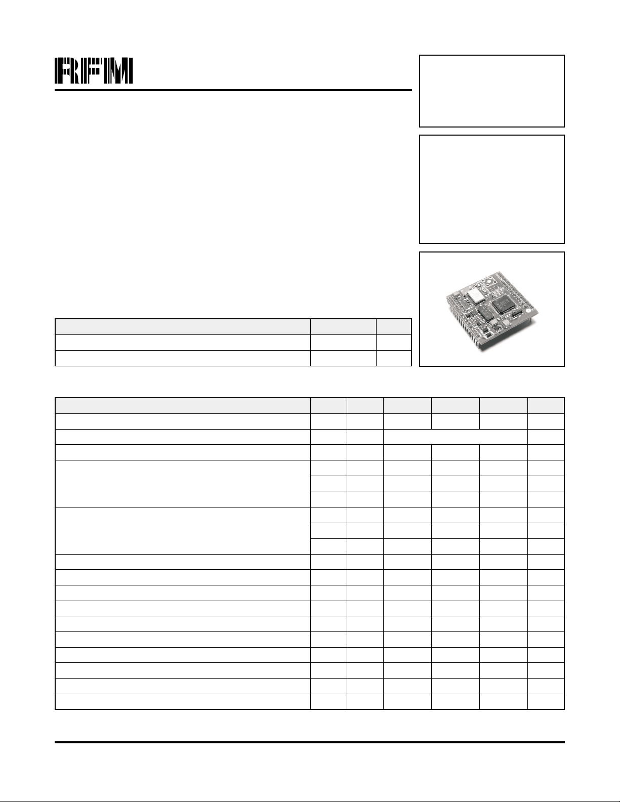
The DM2200-916VM is a 916.5 MHz transceiver module designed for wireless industrial sensor ap
plications. The transceiver module is equipped with two ADC inputs, three digital inputs, two digital
outputs and a serial port. The communication range of the DM2200-916VM in an “open field” envi
ronment is typically 600 meters/hop. The DM2200-916VM combines RFM’s low-current ASH radio
technology with low-power microprocessor technology to achieve very long battery life. The
DM2200-916VM employs RFM’s VersaMESH
bust wireless network routing, an integrated multitasking operating system, and an extensive appli
cation command set. The DM2200-916VM is certified under FCC 15.247 regulations.
Absolute Maximum Ratings
Rating Value Units
All I/O Pins Except VIN -0.3 to +4.0 V
Non-Operating Ambient Temperature Range -50 to +100
TM
V2.0 mesh network protocol, which provides ro
-
o
C
DM2200-
916VM
916.50 MHz
-
-
-
Transceiver
Module
Electrical Characteristics
Characteristic Sym Notes Minimum Typical Maximum Units
Operating Frequency f
Modulation Type OOK on BPSK Spreading Code
RF Encoded Data Transmission Rate 9.6 kb/s
Receive Mode:
Average Input Current, 5 Vdc VIN Supply I
Pulse Input Signal for 10
Transmit Mode:
Peak Input Current, 5 Vdc VIN Supply I
Peak Transmitter Output Power P
Average Sleep Mode Input Current, 5 Vdc VIN Supply I
Analog Input Measurement Range (12-bit ADC) 0 V
External Source Impedance to Analog Input 10 K
Digital Output Source Current, 1K Load 1 mA
Digital Output Sink Current, 1K Load 1.2 mA
Serial Port Data Rate 19.2 kb/s
Internal Power Supply Input Voltage Range 3.1 14.0 Vdc
External Power Supply Voltage Range V
External Power Supply Voltage Ripple 10 mV
Operating Ambient Temperature Range T
-3
BER, 25 °C
O
R
TP
O
S
DD
A
916.30 916.70 MHz
4.5 mA
-102 dBm
32 mA
10 dBm
68 µA
DD
2.9 3.7 Vdc
-40 +85
V
P-P
o
C
1
Page 2

TR 8100
ASH
Transceiver
3 VDC
3 VDC
CFGCLK
CFGDAT
RXDATA
TXM O D
Voltage
Reset
Voltage
Regulator
CFG
RSSI
Low
D M 2 2 0 0 B lo c k D ia g r a m
GRN
YEL
RED
M SP 430F148
M icrocontroller
14
13
12
11
10
9
8
7
6
5
4
3
2
1
J2
GND
GP7
GP6
GP5
GP4
GP3
GP2
GP1
GP0/R SSI
RTS
CTS
TXD
RXD
GND
J1
GND VIN
VREN VDD TD0 TD1 TWS TCK RST CFG0CFG1CFG2CFG3 GND
56789104321
Figure 1
DM2200-916VM Theory of Operation
The major components of the DM2200-916VM include
the TR8100 ASH transceiver and the TI MSP430F148
microcontroller. The TR8100 operates on 916.5 MHz,
with a nominal output power of 10 mW. The MSP430F148 can operate referenced to either a 32.768 kHz
or 6 MHz crystal.
The MSP430F148 UART is used to provide a CMOS
serial interface on connector J2. The microcontroller’s
I/O pins are also available on connector J2 for external
11 12 13 14
monitoring or control. Note that GP0 is dedicated to
measuring the value of the received signal strength
indicator (RSSI) circuit and should always be set as an
analog input. The three LEDs on the transceiver module
display RF communication activity.
DM2200-916VM operation is based on RFM’s multi-
TM
tasking VersaMESH
network protocol, which supports
data and command transfers through both the serial in
TM
terface and the RF channel. See the VersaMESH
Pro
tocol User’s Guide for further details.
-
-
2
Page 3

DM2200-916VM FCC Certification
The DM2200-916VM is certified for operation under
FCC Part 15 Rules, Section 15.247. When the
DM2200-916VM is run from an off-board power supply
(applied to J1-4), the supply voltage must be limited to
a maximum of 3.7 Vdc, and the power supply voltage
ripple must not exceed 10 mV
P-P
.
FCC Labels and Notices
A clearly visible label is required on the outside of the
user’s (OEM) enclosure stating that this product con
tains a DM2200-916VM radio module, FCC ID:
TE6-DM2200A.
This device complies with Part 15 of the FCC rules.
Operation is subject to the following two conditions: (1)
this device may not cause harmful interference, and (2)
this device must accept any interference received, in
cluding interference that may cause undesired opera
-
-
tion.
WARNING: This device operates under Part 15 of the
FCC rules. Any modification to this device, not expressly authorized by RF Monolithics, Inc., may void
the user’s authority to operate this device.
DM2200-916VM Applications
There are two ways to use the DM2200-916VM in an
application. The transceiver module can be used with a
companion application interface board, the IM2200. The
IM2200 has provisions for powering the transceiver
module from a USB cable, an external unregulated DC
supply such as a 5 Vdc “wall” transformer, an external
regulated 3 Vdc power supply, or an external battery.
The IM2200 also provides the choice of UART, RS232,
RS485 (single drop) or USB for a host computer serial
interface. In addition, the IM2200 includes capturedscrew terminal strips for connecting analog inputs, digi
tal logic inputs, digital logic outputs and form C relay
outputs. Refer to the IM2200 data sheet for additional
details.
The DM2200-916VM can also be integrated into the
user’s own application board. The DM2200-916VM pin
descriptions are given in the Table on pages 4 and 5.
The transceiver module pin-out locations are show in
Figure 2, and the PCB layout for the mating connectors
is shown in Figure 3.
The operating range of the DM2200-916VM critically
depends on the antenna being located properly. When
using the standard DM2200-916VM antenna (RFM part
number 400-1687-001), care should be taken to keep
the antenna at least 0.5 inch away from the sides of its
enclosure. The enclosure must be made from a plastic
with low RF attenuation, such as fiberglass, PVC or
ABS. Note: other antenna configurations are possible,
but each new antenna configuration must be added to
the DM2200-916VM FCC module certification before
deployment. Contact RFM for details.
The DM2200-916VM enclosure should be mounted so
the antenna is at least 4 feet off the ground, and ideally
6 or more feet off the ground.
The DM2200-916VM has an on-board regulator input
on Pin J1-2. To use the on-board regulator, connect
J1-3 to J1-2 and apply a voltage to this connection of at
least 3.1 Vdc, but not greater than 14 Vdc, including rip
ple variations. When running from the on-board regula
tor, up to 5 mA is available on J1-4 to operate external
circuitry. Any external circuitry connected to J1-4 must
not induce more that 10 mV
ripple on the regulated
P-P
3 Vdc at this pin.
The DM2200-916VM can also be run from an off-board
regulated supply or a battery. In this case, connect J1-3
to ground, leave J1-2 unconnected, and apply the regulated supply or battery input to J1-4. Note the input voltage range for J1-4 must be in the range of 2.9 to 3.7
Vdc, with no more than 10 mV
P-P
ripple.
Only pins J1-2 and J1-3 are rated to operate from a
supply voltage higher than 3.7 Vdc. Further, care must
be taken so that analog or logic inputs applied to the
transceiver module stay within the voltage range of 0 to
VDD (voltage at J1-4). Applying a voltage outside of the
-
0 to VDD voltage range to an analog or logic input can
damage the module.
The DM2200-916VM has current limiting protection re
sistors on most of the I/O pins. These limit the current
that a logic output can source or sink. Any DM2200-
915.50SN pin defined as an output should be used only
to drive a high impedance load such as a CMOS logic
input or a MOSFET transistor.
-
-
-
3
Page 4

Pin Descriptions
Pin Name Description
J1-1 GND This pin is connected to ground.
J1-2 VIN
J1-3 VREN
J1-4 VDD
J1-5 TD0 This pin is only used for factory programming. It must be left unconnected in normal operation.
J1-6 TDI This pin is only used for factory programming. It must be left unconnected in normal operation.
J1-7 TWS This pin is only used for factory programming. It must be left unconnected in normal operation.
J1-8 TCK This pin is only used for factory programming. It must be left unconnected in normal operation.
J1-9 RST This pin is only used for factory programming. It must be left unconnected in normal operation.
J1-10 CFG0
J1-11 CFG1
J1-12 CFG2
J1-13 CFG3
This pin is the input to the DM2200-916VM on-board voltage regulator. The minimum input voltage to this pin is
3.1 V, and the maximum input to this pin is 14.0 V.
This pin is the enable input for the DM2200-916VM on-board regulator. To enable the on-board regulator, con
nect this pin to J1-2. To disable the on-board regulator, connect this pin to ground.
This pin is connected to the DM2200-916VM positive power supply buss. When the module is powered from
the on-board regulator, this pin can provide up to 5 mA of current at 3.0 Vdc. Note this current adds to the re
ceive, transmit and sleep currents listed in the specifications on Page 1. The external load must not impress
more than 10 mV peak -peak ripple on the supply buss. If the on-board regulator is disabled, the module can be
powered through this pin by an external 2.9 to 3.7 Vdc source (maximum ripple 10 mV peak-peak).
This pin is a hardware configuration input, reserved for future use. Connect it to J1-4 (positive supply buss) for
normal operation.
This pin is a hardware configuration input, reserved for future use. Connect it to J1-4 (positive supply buss) for
normal operation.
This pin is a hardware configuration input, reserved for future use. Connect it to J1-4 (positive supply buss) for
normal operation.
This pin is a hardware configuration input, reserved for future use. Connect it to J1-4 (positive supply buss) for
normal operation.
-
-
J1-14 GND This pin is connected to ground.
J2-1 GND This pin is connected to ground.
J2-2 RXD This pin is the serial data input (CMOS).
J2-3 TXD This pin is the serial data output (CMOS).
J2-4 CTS This pin is a serial data flow control input (CMOS). Hardware flow control is required.
J2-5 RTS This pin is a serial data flow control output (CMOS). Hardware flow control is required.
J2-6 GP0/RSSI
J2-7 GP1
J2-8 GP2
J2-9 GP3 This pin is an I/O pin. The default configuration of this pin is a digital input.
J2-10 GP4 This pin is an I/O pin. The default configuration of this pin is a digital output.
J2-11 GP5 This pin is an I/O pin. The default configuration of this pin is a digital output.
J2-12 GP6 This pin is an I/O pin. The default configuration of this pin is an analog-to-digital converter input.
J2-13 GP7 This pin is an I/O pin. The default configuration of this pin is an analog-to-digital converter input.
J2-14 GND This pin is connected to ground.
This pin is an I/O pin dedicated to monitoring the RSSI circuit output. It is configured as an analog-to-digital
converter input. The RSSI signal can also be monitored externally at this pin.
This pin is an I/O pin. The default configuration of this pin is a digital input with optional pulse counting capabil
ity. A 24-bit register is maintained within the DM2200 to accumulate pulse counts. This input can count up to
10 pulses/second. This input supports interrupts, allowing pulse counting or alarm monitoring while the DM2200
is operating in a low current “sleep” mode.
This pin is an I/O pin. The default configuration of this pin is a digital input. This input supports interrupts, allow
ing alarm monitoring while the DM2200 is operating in a low current “sleep” mode.
-
-
4
Page 5

D M 2200 Pin O ut
GND
CFG3
CFG2
CFG1
CFG0
RST
TCK
TW S
TD1
TD0
VDD
VREN
VIN
GND
GND
GP7
GP6
GP5
GP4
GP3
GP2
GP1
GP0/RSSI
RTS
CTS
TXD
RXD
GND
Figure 2
CAUTION: Electrostatic Sensitive Device. Observe precautions when handling.
5
Page 6

D M 2200 Interface C onnector
PC B Layout D etail
0.2
(5 .1 )
0.1
(2 .5 )
1.4
(3 5 .6 )
J1 J2
1.3
(3 3 .0 )
1.4
(3 5 .6 )
C onnectors are FC I E lectronics 66951-014 or equivalent
D im ensions in inches and (m m )
Figure 3
Note: Specifications subject to change without notice.
file: dm2200i.vp, 2006.04.29 rev
6
 Loading...