

Page 1
®
Preliminary
Base Station with Host Serial Interface
•
Compatible with RFM miniMESHTMNetwork Protocol
•
3 V, Very Low Current Operation
•
Ready-to-Use OEM Module
•
DM1800-
916MB
916.50 MHz
The DM1800-916MB is the 916.50 MHz base station module in the DM1800 family of RF transceiv
ers. The DM1800 family is designed for adding embedded wireless connectivity to a wide range of
monitoring and control systems. The DM1800-916MB is equipped with a serial I/O port to interface
to a host microcontroller. The module also includes an analog input, a logic input, and a logic output
for local monitoring and control. Radio communications range in an “open field” environment is typi
cally 200 meters/hop. The DM1800-916MB combines RFM’s very low current ASH radio technol
ogy with low power microcontroller technology to achieve long battery life. This module is
compatible with RFM’s miniMESH
multicast mesh network routing. The DM1800-916MB is certified for operation under FCC 15.249
regulations.
Absolute Maximum Ratings
All Input/Output Pins Except VIN -0.3 to +3.3 V
Non-Operating Ambient Temperature Range -50 to +100
Electrical Characteristics
Operating Frequency f
Modulation Type OOK
RF Encoded Data Transmission Rate 4.8 kb/s
Average Receiver Input Current, No External Power Supply Load I
Receiver Input Signal for 10
Peak Transmitter Input Current, No External Power Supply Load I
Peak Transmitter Output Power P
Analog Input Measurement Range (10-bit ADC) 0 VOUT V
Source Impedance to Analog Input 10 K
Digital In Logic High 2.4 V
Digital In Logic Low .45 V
Digital Out Logic High, No Load 2.4 V
Digital In Logic Low, No Load 0.3 V
Digital Output Source Current, 1K load 1.1 mA
Digital Output Sink Current, 1K load 1.2 mA
Serial Port Data Rate 9.6 kb/s
Power Supply Input Voltage Range, -40 to +85
Power Supply Input Voltage Range, 0 to +85
Regulated Power Supply Output Voltage, VIN 3.1 to 14 V VOUT 3.0 Vdc
Regulated Power Supply Voltage Ripple 10 mV
TM
network protocol, which provides add-on “plug-and-play”
Rating Value Units
Characteristic Sym Notes Minimum Typical Maximum Units
O
R
-3
BER, 25 °C
TP
O
o
C VIN 2.6 14 V
o
C VIN 3.1 14 V
-
Module
-
-
o
C
916.30 916.70 MHz
4mA
-98 dBm
13.5 mA
1mW
Transceiver
P-P
1
Page 2
G N D
G N D
J 2 - 3
J 2 - 2
J 2 - 1
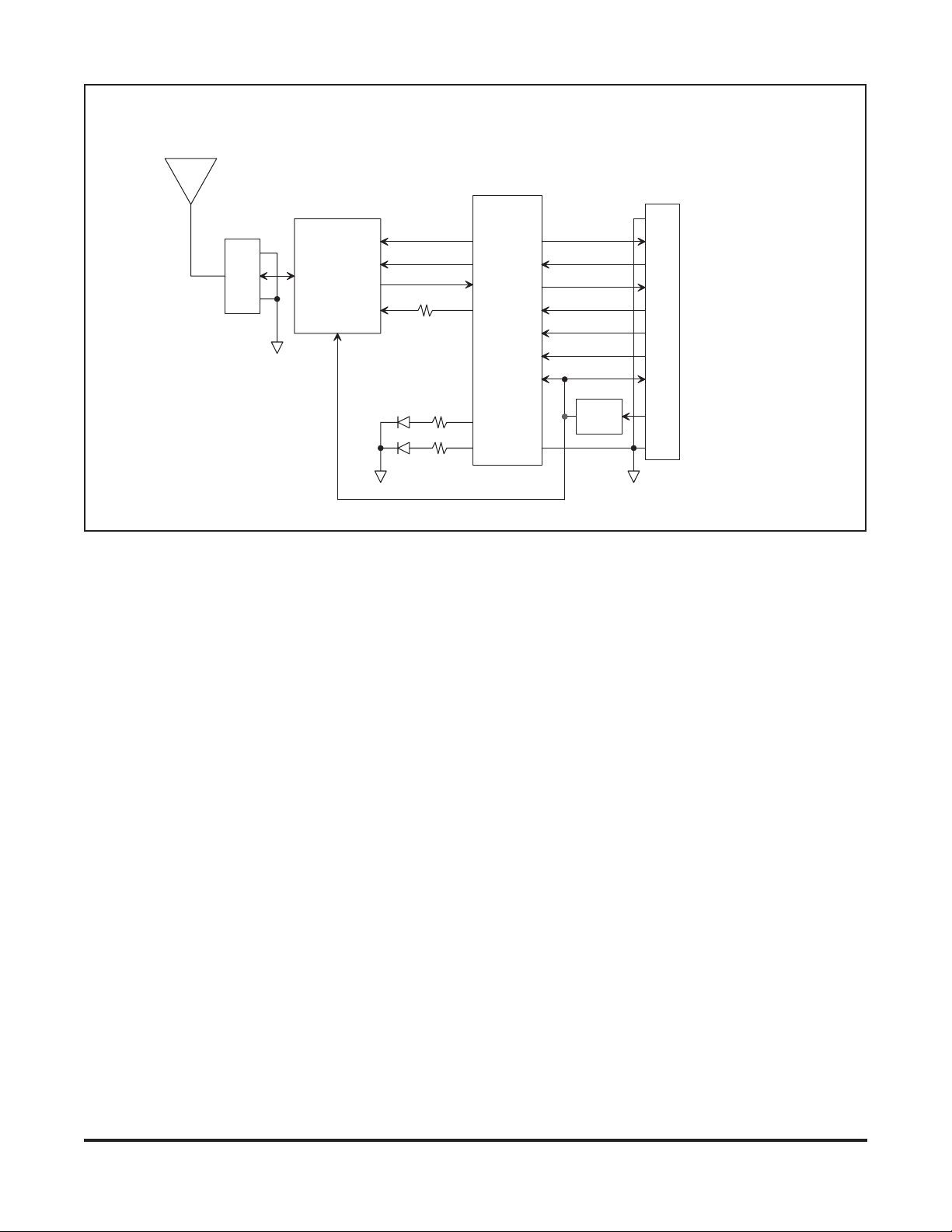
D M 1 8 0 0 - 9 1 6 M B B l o c k D i a g r a m
C N T R L 0
A S H
T r a n s c e i v e r
C N T R L 1
R X D A T A
T X M O D
P I C
1 6 F 6 8 8
µ P
J 1 - 1 0
J 1 - 9
J 1 - 8
J 1 - 7
J 1 - 6
J 1 - 5
J 1 - 4
J 1 - 3
G N D
S E R I A L T X
S E R I A L R X
D I G I T A L O U T
A N A L O G I N
D I G I T A L I N
B I N D
V O U T
L E D 1
L E D 2
Figure 1
Theory of Operation
The major components of the DM1800-916MB include
an RFM TR1000 ASH transceiver and a Microchip
PIC16F688 microcontroller. The TR1000 operates on
a frequency of 916.50 MHz, at a nominal output power
of 1 mW.
The 16F688 provides a 9.6 kb/s serial interface for
communication with a host microcontroller. A compan
ion interface board is available with USB bridge cir
cuitry to interface the DM1800-916MB to a host PC.
Three of the 16F688 I/O pins are configured for exter
nal monitoring or control. Digital In is configured as a
logic input with a weak pull-up for sensing a contact
closure to a ground pad. Digital Out is configured a
logic output. Analog In is configured as a 10-bit ana
log-to-digital input. The DM1800 includes two LEDs
that indicate the module’s operating mode.
The DM1800-916MB is compatible with RFM’s
TM
miniMESH
network protocol, which provides add-on
“plug-and-play” mesh network routing to improve com
munication range and robustness.
DM1800-916MB FCC Certification
The DM1800-916MB hardware has been certified for
operation under FCC Part 15 Rules, Section 15.249.
3 V
R e g
J 1 - 2
J 1 - 1
V I N
G N D
This certification applies only when a DM1800-916MB
is equipped with one of the following RFM antennas:
helical antenna, RFM part number 500-1195-003
helical antenna, RFM part number 500-1195-103
WARNING: the DM1800-916MB must be re-certified
if used with any antennas other than the two listed
-
above. Contact RFM for further information if your ap
plication requires a special antenna configuration.
FCC Notices and Labels
-
This device complies with Part 15 of the FCC rules.
Operation is subject to the following two conditions:
(1) this device may not cause harmful interference,
and (2) this device must accept any interference re
ceived, including interference that may cause unde
sired operation.
A clearly visible label is required on the outside of the
user’s (OEM) enclosure stating that this product con
-
tains a DM1800-916MB transceiver assembly, FCC
ID: TE6-DM1800.
WARNING: This device operates under Part 15 of the
FCC rules. Any modification to this device, not expressly authorized by RF Monolithics, Inc., may void
the user’s authority to operate this device.
-
-
-
-
2
Page 3

DM1800-916MB I/O Pad Descriptions
Pin Name Description
J1-1 GND This pad is a signal and power supply ground.
J1-2 VIN This is the power supply input pad. The allowed input voltage range is 2.6 to 14 V.
VOUT tracks 50 to 100 mV below VIN when VIN is in the range of 2.6 to 3.1 V. When VIN is in the range of 3.1
J1-3 VOUT
J1-4 BIND
J1-5 DIGITAL IN
J1-6 ANALOG IN
to 14 V, VOUT is regulated at 3.0 Vdc. Up to 10 mA can be supplied from this pad for powering external circuits
such as thermistor-resistor networks. External circuitry must not impress more than 10 mV
lated output voltage.
This pad is connected to a logic input on the microcontroller, and is configured with a weak pull-up. When this pin
is momentarily grounded (to J1-1 or J1-10, the module is placed into the bind mode, allowing this module to be
associated with other modules to form a network.
This pad is connected to a logic input on the microcontroller, and is configured with a weak pull-up, allowing
both logic signals and contact closures referenced to J-1 or J-10 to be read. The value of this input is sent over
the RF channel as a response to an RF command. The input voltage range on this pad is 0 to VOUT. Applying
a voltage outside of this range may damage the module.
This pad in the input to the microcontroller’s 10-bit analog-to-digital (ADC) converter. The ADC input range is 0
to VOUT, referenced to J1-1 or J1-10. The input voltage range on this pad is 0 to VOUT. Applying a voltage
outside of this range may damage the module. The ADC reading is sent over the RF channel as a response to
an RF command.
ripple on the regu
p-p
-
J1-7 DIGITAL OUT
short-circuit protection. The value of this output is set or read over the RF channel as a response to an RF com
mand.
This pad is connected to the module’s serial data input (USART). Data to this pin is received at 9.6 kb/s, using
This pad is connected to a logic output on the microcontroller through a 1 kilohm resistor, which provides
J1-8 SERIAL RX
8 data bits, no parity, and one stop bit. The input voltage range on this pad is 0 to VOUT. Applying a voltage
outside of this range may damage the module.
J1-9 SERIAL TX
This pad is connected to the module’s serial data output (USART) through a 1 kilohm resistor, which provides
short-circuit protection. Data from this pad is sent at 9.6 kb/s, using 8 data bits, no parity, and one stop bit.
J1-10 GND This pad is a signal and power supply ground.
J2-1 GND This pad is a ground for the antenna port.
J2-2 ANT This pad is the antenna port.
J2-3 GND This pad is a ground for the antenna port.
-
3
Page 4

D M 1 8 0 0 - 9 1 6 M B I / O P a d L a b e l s
G N D
S E R I A L T X
G N D
R F I O
G N D
Figure 2
D M 1 8 0 0 - 9 1 6 M B S M T M o u n t i n g P a t t e r n
. 0 9 5
1 . 5 3 5
. 0 8 0
S E R I A L R X
D I G I T A L O U T
A N A L O G I N
D I G I T A L I N
B I N D
V O U T
V I N
G N D
. 2 0 0
1 . 0 0 0
. 1 3 0 . 0 9 0. 0 9 0
. 2 0 0
D i m e n s i o n s i n i n c h e s . P C B p l u s c o m p o n e n t h e i g h t i s . 1 7 0 m a x ;
Note: Specifications subject to change without notice.
. 1 0 0 T Y P
. 0 5 0
. 0 7 0 T Y P
P C B p l u s a n t e n n a h e i g h t i s 1 . 1 5 m a x
Figure 3
file: dm1800_916bk.vp, 2005.12.07 rev
4
 Loading...