


ISED Canada Radio Standards Specification: RSS-247
Certification Exhibit
FCC ID: HSW2832
IC: 4492A-2832
FCC Rule Part: 15.247
Project Number: 72126480
Manufacturer: Murata Electronics North America
Model: MBN52832
Manual
5015 B.U. Bowman Drive Buford, GA 30518 USA
©2017 by Murata Electronics N.A., Inc.
MBN52832 Data Sheet, v0.92, 08/23/2017 www.murata.com
Revision History
Revision
Date
Author
Change Description
0.1
06/03/2016
RF PD
Preliminary version
0.2
06/16/2016
RF PD
Modified the module block diagram.
0.3
8/25/2016
RF PD
Update test data points
0.4
8/27/2016
RF PD
Update module dimension and reference schematic
0.5
12/15/2016
RF PD
Applied model/type name MBN52832 to the datasheet
0.6
02/01/2017
RF PD
Update Table 2.1 and Figure 2.2
0.7
03/15/2017
RF PD
Add sleep current
0.8
05/26/2017
RF PD
Table 2.2, change pin 36, 37 pin 36 description to NC.
Add section 6.1 and 6.2, recommendation for host PCB landing and
placement.
Updated reference schematic.
Add section 8 and section 9, assembly and packaging information.
Add section 12 Notice.
Add section 13 Preconditions to use the module.
0.9
07/27/2017
RF PD
Add regulatory section
0.92
8/23/2017
RF PD
Update layout guidance for antenna connection; updated regulatory
information
MBN52832 Data
BLE Module

©2017 by Murata Electronics N.A., Inc.
MBN52832 Data Sheet, v0.92, 08/23/2017 Page 2 of 35 www.murata.com
Table of Contents
REVISION HISTORY .............................................................................................................................................................. 1
TABLE OF CONTENTS ......................................................................................................................................................... 2
1 INTRODUCTION ............................................................................................................................................................ 5
1.1 Features ..................................................................................................................................................................... 5
1.2 Applications ................................................................................................................................................................ 5
1.3 Block Diagram ............................................................................................................................................................ 6
1.4 Acronyms ................................................................................................................................................................... 6
1.5 References ................................................................................................................................................................. 6
2 MECHANICAL SPECIFICATION .................................................................................................................................. 7
2.1 Module Dimensions .................................................................................................................................................... 7
2.2 Top and Side View ..................................................................................................................................................... 7
2.3 PCB Footprint Top View ............................................................................................................................................. 8
2.4 Pin Configuration ........................................................................................................................................................ 9
3 DC ELECTRICAL SPECIFICATION ............................................................................................................................ 12
3.1 Typical Power Consumption .................................................................................................................................... 12
4 RF SPECIFICATION .................................................................................................................................................... 12
5 ENVIRONMENTAL SPECIFICATION ......................................................................................................................... 13
5.1 Absolute Maximum Rating ....................................................................................................................................... 13
5.2 Recommended Operating Condition ........................................................................................................................ 13
6 POWER SEQUENCE ................................................................................................................................................... 13
8 APPLICATION INFORMATION ................................................................................................................................... 14
8.1 Recommended PCB Landing Pattern ...................................................................................................................... 14
8.2 Host PCB Layout Recommendations ...................................................................................................................... 15
8.3 Layout Guidance for Using Internal PCB Antenna .................................................................................................. 16
8.4 Layout Guidance for Microstrip Design And External Antenna ................................................................................ 17
9 APPLICATION REFERENCE ...................................................................................................................................... 20
10 ASSEMBLY INFORMATION ....................................................................................................................................... 21
11 PACKAGING AND MARKING INFORMATION .......................................................................................................... 22
11.1 Dimensions of Tape (Plastic tape) ........................................................................................................................... 22
11.2 Dimensions of Reel .................................................................................................................................................. 23
11.3 Taping Diagrams ...................................................................................................................................................... 24
11.4 Leader and Tail tape ................................................................................................................................................ 25
11.5 Peeling Force ........................................................................................................................................................... 26
11.6 PACKAGE (Humidity proof Packaging) ................................................................................................................... 26
11.7 Module Marking Information..................................................................................................................................... 27
11.8 Moisture Sensitivity Level ......................................................................................................................................... 27
12 REGULATORY INFORMATION .................................................................................................................................. 28
12.1 FCC Notice (USA) .................................................................................................................................................... 28
12.2 FCC Labeling Requirements .................................................................................................................................... 29
12.3 IC Notice (Canada) .................................................................................................................................................. 29
12.4 IC Labeling Requirements........................................................................................................................................ 30
12.5 ESTI compliance (Europe) ....................................................................................................................................... 30
12.6 RF Exposure ............................................................................................................................................................ 30

©2017 by Murata Electronics N.A., Inc.
MBN52832 Data Sheet, v0.92, 08/23/2017 Page 3 of 35 www.murata.com
13 ROHS INFORMATION ................................................................................................................................................. 30
14 ORDERING INFORMATION ........................................................................................................................................ 31
15 NOTICE ........................................................................................................................................................................ 32
15.1 Storage Conditions ................................................................................................................................................... 32
15.2 Handling Conditions ................................................................................................................................................. 32
15.3 Standard PCB Design (Land Pattern and Dimensions) ........................................................................................... 32
15.4 Notice for Chip Placer .............................................................................................................................................. 32
15.5 Operational Environment Conditions ....................................................................................................................... 32
15.6 Input Power Capacity ............................................................................................................................................... 33
16 PRECONDITIONS TO USE MURATA PRODUCTS ................................................................................................... 34
17 TECHNICAL SUPPORT CONTACT ............................................................................................................................ 35

©2017 by Murata Electronics N.A., Inc.
MBN52832 Data Sheet, v0.92, 08/23/2017 Page 4 of 35 www.murata.com
LIST OF FIGURES
Figure 1.1 Block Diagram ........................................................................................................................................................ 6
Figure 2.1 Module Top and Side View (Unit: mm) .................................................................................................................. 7
Figure 2.2 Module Footprint Top View (Unit: mm) .................................................................................................................. 8
Figure 2.3 Pinout Diagram Top View ...................................................................................................................................... 9
Figure 8.1 Recommended PCB Landing Pattern.................................................................................................................. 14
Figure 8.2 Host PCB Layout Recommendation, top view ..................................................................................................... 15
Figure 8.3 Layout Guide for Antenna Performance (1) ......................................................................................................... 16
Figure 8.4 Layout Guide for Antenna Performance (2) ......................................................................................................... 17
Figure 8.5 Layout Guide for External Antenna (1) ................................................................................................................ 18
Figure 8.6 Layout Guide for External Antenna (2) ................................................................................................................ 18
Figure 9.1 Reference Design ................................................................................................................................................ 20
Figure 10.1 Reflow Profile ..................................................................................................................................................... 21
Figure 11.1 Tape Dimensions (Unit in mm) .......................................................................................................................... 22
Figure 11.2 Reel Dimensions (Unit: mm) .............................................................................................................................. 23
Figure 11.3 Tape Diagram .................................................................................................................................................... 24
Figure 11.4 Tape Leader and Tail ......................................................................................................................................... 25
Figure 11.5 Peeling Force Diagram ...................................................................................................................................... 26
Figure 11.6 Packaging Diagram............................................................................................................................................ 26
Figure 11.7 Module Marking Diagram ................................................................................................................................... 27
LIST OF TABLES
Table 2.1: Module Dimensions ................................................................................................................................................ 7
Table 2.2 Pinouts .................................................................................................................................................................. 10
Table 3.1 Typical Power Consumption ................................................................................................................................. 12
Table 4.1 RF Characteristics ................................................................................................................................................. 12
Table 5.1 Absolute Maximum Rating .................................................................................................................................... 13
Table 5.2 Recommended Operating Condition ..................................................................................................................... 13
Table 12.1 Regulatory Standards Conformance................................................................................................................... 28
Table 12.2 External Antenna to comply with FCC and IC .................................................................................................... 28
Table 12.3 External Antenna to comply with IC .................................................................................................................... 29

©2017 by Murata Electronics N.A., Inc.
MBN52832 Data Sheet, v0.92, 08/23/2017 Page 5 of 35 www.murata.com
1 Introduction
MBN52832 is a Bluetooth Low Energy module. It enables ultra-low power connectivity for data communication. The
product integrates Nordic Bluetooth Low Energy IC, RF front end, and crystal. This is an ideal solution for Internet of
Things (IOT) application.
1.1 Features
• Bluetooth® v5, ANT, NFC Tag
• Nordic nRF52832 Bluetooth Smart®
• Built-in ARM Cortex M4 core with 64KB RAM and 512KB flash
• Dimension 7.4 x 7.0 x 1.0 mm
• Packaging: LGA
• Bluetooth/ANT Antenna Configuration:
o On-board PCB antenna
o Supports external antenna from pin pad
• Maximum transmit power: +3.5dBm (@ antenna port)
• Receive sensitivity: -90dBm @ 1Mbps (DCDC Mode)
• Power consumption
o TX 7mA @ 3.5dBm (DCDC Mode)
o RX 6mA* (DCDC Mode)
• Host interface: UART, SPI
• Other interfaces: 20 GPIO, 5 ADC, UART, SPI (master and slave), I2C, PWM and Debug SWD
• Operating temperature range: -40 ºC to 85 ºC
• RoHS compliant
• MSL Level 3 in accordance with JEDEC J-STD-020
• Regulatory certificates: FCC, IC, ETSI (plan)
1.2 Applications
• Home Automation
• Proximity Services
• Building automation
• Medical/Healthcare
• Beacon
©2017 by Murata Electronics N.A., Inc.
MBN52832 Data Sheet, v0.92, 08/23/2017 Page 6 of 35 www.murata.com
1.3 Block Diagram
Figure 1.1 Block Diagram
1.4 Acronyms
- AIO Analog Input / Output
- GPIO General Purpose Input / Output
- I2C Inter-Integrated Circuit
- LPCOMP Low Power Comparator
- SPI Serial Peripheral Interface
- UART Universal Asynchronous Receiver Transmitter
1.5 References
[1] Nordic Semiconductor, nRF52832 - Product Specification v1.3, 2017
[2] Nordic Semiconductor, nRF52832-CIAA Pin assignment and mechanical dimensions, 2016
VCC
UART
SWD
GPIO/AIO
SPI
Nordic
nRF52832
32MHz X’tal
Matching
circuit
32KHz X’tal
(for ANT only
NFC Antenna
(Optional)
BLE/ANT
Antenna
To external or
on-board
antenna
Inductor for DC/DC
(optional)

©2017 by Murata Electronics N.A., Inc.
MBN52832 Data Sheet, v0.92, 08/23/2017 Page 7 of 35 www.murata.com
2 Mechanical Specification
2.1 Module Dimensions
Table 2.1: Module Dimensions
Parameter
Typical
Unit
Dimension (L x W x H)
7.4 ±0.2mm x 7.0 ±0.2mm x 1.0 (max)
mm
2.2 Top and Side View
Figure 2.1 Module Top and Side View (Unit: mm)
Pin 1
7.0mm typ.
1.0mm
max.
7.4mm typ.
©2017 by Murata Electronics N.A., Inc.
MBN52832 Data Sheet, v0.92, 08/23/2017 Page 8 of 35 www.murata.com
2.3 PCB Footprint Top View
Figure 2.2 Module Footprint Top View (Unit: mm)
©2017 by Murata Electronics N.A., Inc.
MBN52832 Data Sheet, v0.92, 08/23/2017 Page 9 of 35 www.murata.com
2.4 Pin Configuration
Figure 2.3 Pinout Diagram Top View
©2017 by Murata Electronics N.A., Inc.
MBN52832 Data Sheet, v0.92, 08/23/2017 Page 10 of 35 www.murata.com
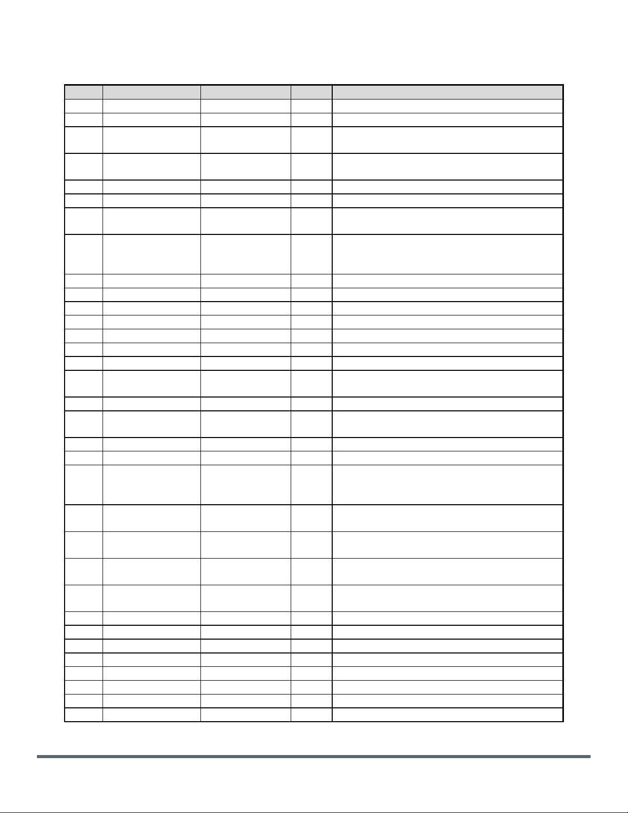
Table 2.2 Pinouts
Pin #
Pin Name
Nordic IC Pin
I/O
Description
1
P0_09/NFC ANT
P0.09/NFC
I/O
GPIO; NFC antenna connection.
2
P0_06
P0.06
I/O
GPIO
3
P0_00/XL1
P0.00/XL1
I/O
Connection for 32.768kHz crystal (LFXO);
GPIO
4
P0_01/XL2
P0.01/XL2
I/O
Connection for 32.768kHz crystal (LFXO);
GPIO
5
GND
GND
6
VCC
VDD
Module power supply
7
DCC
DCC
DC/DC converter output pin. *Refer to
reference schematic.
8
DEC
DEC4
1V3 regulator supply decoupling. Input from
DC/DC converter. Output from 1.3V LDO.
*Refer to reference schematic.
9
P0_02/AIN0
P0.02/AIN0
I/O
GPIO; SAADC/COMP/LPCOMP input
10
P0_05/AIN3
P0.05/AIN3
I/O
GPIO; SAADC/COMP/LPCOMP input
11
P0_03/AIN1
P0.03/AIN1
I/O
GPIO; SAADC/COMP/LPCOMP input
12
P0_04/AIN2
P0.04/AIN2
I/O
GPIO; SAADC/COMP/LPCOMP input
13
P0_29/AIN5
P0.29/AIN5
I/O
GPIO; SAADC/COMP/LPCOMP input
14
P0_07
P0.07
I/O
GPIO
15
P0_08
P0.08
I/O
GPIO
16
SWDIO
SWDIO
I/O
Serial Wire Debug I/O for debug and
programming.
17
P0_21/RESET
P0.21/RESET
I/O
GPIO; Configurable as system RESET pin
18
SWDCLK
SWDCLK
I/O
Serial Wire Debug clock input for debug
and programming.
19
GND
GND
GND
20
ANTIN
*Refer to reference schematic.
21
ANTOUT
RF signal output. Connect to ANTIN for onboard antenna or to external antenna.
*Refer to reference schematic.
22
P0_18/TRACE0
P0.18/TRACE
DATA[0]
I/O
GPIO; Trace port output;
23
P0_16/TRACE1
P0.16/TRACE
DATA[1]
I/O
GPIO; Trace port output.
24
P0_15/TRACE2
P0.15/TRACE
DATA[2]
I/O
GPIO; Trace port output.
25
P0_14/TRACE3
P0.14/TRACE
DATA[3]
I/O
GPIO; Trace port output.
26
P0_10/NFC ANT
P0.10/NFC
I/O
GPIO; NFC antenna connection.
27
P0_20
P0.20
I/O
GPIO
28
P0_17
P0.17
I/O
GPIO
29
P0_13
P0.13
I/O
GPIO
30
GND
Ground.
31
GND
Ground.
32
GND
Ground.
33
GND
Ground.
 Loading...