

Page 1

Bluetooth Class 1 Module
SN2100
User Manual
And Datasheet
Version: 1.1
June 25, 2013
Note: SyChip, L.L.C. reserves the right to make changes in specifications at any time and without notice. The
information furnished in this data sheet is believed to be accurate and reliable. However, no responsibility is assumed
by SyChip for its use, nor any infringements of pa tents or othe r rights of third parties resulting from its use. No license
is generated under any rights of SyChip or its supporters unless specifically agreed.
Page 2
Revision History
Revision Date Author Change Description
0.1 Jul-07-2011 Release the first datasheet.
0.5 Nov-15-2011 N. Nagayama Update the block diagram / BT IC product number
Update the SyChip Part Number
0.6 Jan-05-2012 Viet H. Update the spec table
0.61 Jan-31-2012 Y Fang Added disclaimer
0.62 Apr-10-2012 JAG Added packaging, labeling and regulatory information
0.63 May-22-2012 Viet H. Update the spec table
1.0 Aug-10-2012 Y Fang Added Software and Development Tool sections
1.1 Jun-25-2013 Y Fang Added Recommended host (customer) circuit board PCB
pattern
SyChip/Murata Confidential Page 2 of 31 SN2100 Datasheet Ver. 1.1
Page 3

Table of Contents
1 SYSTEM DESCRIPTIONS ..................................................................................................................................... 6
1.1 APPLICATIONS ........................................................................................................................................................ 6
1.2 MODULE SUMMARY ............................................................................................................................................... 6
1.3 BLOCK DIAGRAM ................................................................................................................................................... 7
2 MECHANICAL SPECIFICATIONS ..................................................................................................................... 8
2.1 MODULE DIMENSION .............................................................................................................................................. 8
2.2 MODULE TOP AND SIDE VIEW ................................................................................................................................. 8
2.3 MODULE BOTTOM VIEW .......................................................................................................................................... 9
2.4 DETAILED MECHANICAL DATA (TOP VIEW) ........................................................................................................... 10
2.5 MODULE PIN-OUT ................................................................................................................................................. 11
3 DC ELECTRICAL SPECIFICATIONS .............................................................................................................. 13
3.1 TYPICAL POWER CONSUMPTION ........................................................................................................................... 13
3.2 DIGITAL IO SPECIFICATION .................................................................................................................................. 13
4 RF SPECIFICATIONS .......................................................................................................................................... 14
4.1 BLUETOOTH SPECIFICATION ................................................................................................................................. 14
4.2 RF CHARACTERISTICS (TX) ................................................................................................................................. 14
4.3 RF CHARACTERISTICS (RX) ................................................................................................................................. 16
5 ENVIRONMENTAL SPECIFICATIONS ........................................................................................................... 17
5.1 ABSOLUTE MAXIMUM RATINGS ............................................................................................................................ 17
5.2 OPERATION CONDITIONS ...................................................................................................................................... 17
6 APPLICATION INFORMATION ........................................................................................................................ 18
6.1 RECOMMENDED HOST (CUSTOMER) CIRCUIT BOARD PCB PATTERN ..................................................................... 18
6.2 HOST PCB LAYOUT RECOMMENDATIONS ............................................................................................................. 18
6.3 MODULE LOCATION ............................................................................................................................................. 19
6.3.1 Location in x-y plane ............................................................................................................................... 19
6.3.2 Location in z-plane .................................................................................................................................. 21
7 SOFTWARE ........................................................................................................................................................... 22
7.1 SOFTWARE ARCHITECTURE .................................................................................................................................. 22
7.2 BLUETOOTH PROFILE STACKS .............................................................................................................................. 22
8 DEVELOPMENT TOOLS .................................................................................................................................... 23
9 ASSEMBLY INFORMATION ............................................................................................................................. 24
9.1 LEAD-FREE SOLDERING REFLOW PROFILE ............................................................................................................. 24
10 PACKAGING AND MARKING INFORMATION ............................................................................................ 25
10.1 CARRIER TAPE DIMENSIONS ............................................................................................................................ 25
10.2 MODULE MARKING INFORMATION .................................................................................................................. 25
11 ORDERING INFORMATION ............................................................................................................................. 26
12 ROHS DECLARATION ........................................................................................................................................ 26
13 REGULATORY INFORMATION ....................................................................................................................... 26
13.1 FCC NOTICE (USA) ........................................................................................................................................ 26
13.2 FCC LABELING REQUIREMENTS ...................................................................................................................... 27
SyChip/Murata Confidential Page 3 of 31 SN2100 Datasheet Ver. 1.1
Page 4

13.3 RF EXPOSURE .................................................................................................................................................. 27
13.4 IC NOTICE (CANADA) ...................................................................................................................................... 27
13.5 IC LABELING REQUIREMENTS ......................................................................................................................... 28
13.6 CE NOTICE (EUROPE) ...................................................................................................................................... 28
13.7 CE LABELING REQUIREMENTS ........................................................................................................................ 28
14 TECHNICAL SUPPORT CONTACT ................................................................................................................. 29
15 DISCLAIMER ......................................................................................................................................................... 29
SyChip/Murata Confidential Page 4 of 31 SN2100 Datasheet Ver. 1.1
Page 5

LIST OF FIGURES
FIGURE 1 SN2100 MODULE BLOCK DIAGRAM .................................................................................................................. 7
FIGURE 2 MODULE TOP AND SIDE VIEW ............................................................................................................................ 8
FIGURE 3 MODULE BOTTOM VIEW ..................................................................................................................................... 9
FIGURE 4 DETAILED MECHANICAL DATA (TOP VIEW) ....................................................................................................... 10
FIGURE 5 RECOMMENDED HOST (CUSTOMER) PCB PATTERN ........................................................................................ 18
FIGURE 6 RECOMMENDED HOST CIRCUIT BOARD DESIGN UNDERNEATH THE MODULE ................................................ 19
FIGURE 7 RECOMMENDED LOCATIONS IN XY-PLANE ....................................................................................................... 20
FIGURE 8 LOCATIONS NOT RECOMMENDED IN XY-PLANE ............................................................................................... 20
FIGURE 9 RECOMMENDED LOCATIONS IN Z-PLANE .......................................................................................................... 21
FIGURE 10 LOCATIONS NOT RECOMMENDED IN XY-PLANE ............................................................................................. 21
FIGURE 11 REFLOW PROFILE PATTERN .......................................................................................................................... 24
FIGURE 12 CARRIER TAPE DIMENSIONS .......................................................................................................................... 25
FIGURE 13 MODULE MARKING DETAIL ............................................................................................................................. 25
LIST OF TABLES
TABLE 1 MODULE CONNECTOR SIGNAL DESCRIPTION .................................................................................................... 11
TABLE 2 TYPICAL POWER CONSUMPTION ........................................................................................................................ 13
TABLE 3 DIGITAL IO SPECIFICATION ................................................................................................................................ 13
TABLE 4 RF SPECIFICATIONS ........................................................................................................................................... 14
TABLE 5 RF SPECIFICATIONS ........................................................................................................................................... 16
TABLE 6 ABSOLUTE MAXIMUM RATING ............................................................................................................................ 17
TABLE 7 RECOMMENDED OPERATING CONDITIONS ........................................................................................................ 17
TABLE 8 BLUETOOTH STACK AVAILABILITY ..................................................................................................................... 22
TABLE 9 DEVELOPMENT TOOLS ........................................................................................................................................ 23
TABLE 10 REFLOW PROFILE RECOMMENDATION ........................................................................................................... 24
TABLE 11 ORDERING INFORMATION ................................................................................................................................. 26
SyChip/Murata Confidential Page 5 of 31 SN2100 Datasheet Ver. 1.1
Page 6

1 System Descriptions
1.1 Applications
SN2100 is a complete industrial grade high power (class 1) Bluetooth® module with onboard antenna for M2M application. It integrates Bluetooth® IC, PA, RF front end, TCXO
and chip antenna into a small LGA form factor and can be simply dropped into the OEM’s
design. The SN2100 offers total 110 dB link budget, which is significantly better than most
of the Bluetooth® modules do in the market. This makes it a good fit for industrial control
application that usually requires longer distance coverage. The module offers extended
product life and industrial standard operating temperature range to fit the industrial usage.
The SN2100 offers standard HCI interface to the host CPU.
1.2 Module Summary
• Bluetooth V2.0
• Power Grade: Class 1
• Dimensions: 17.5mm x 16.0mm x 2.0 mm
• Supply voltage: 2.2V to 3.3V
• Antenna: on-module
• 32kHz clock circuit : on-module
• Host Interface : UART/PCM
• RoHS compliant
• MSL JEDEC level 3
• FCC/IC certified; CE compliant
SyChip/Murata Confidential Page 6 of 31 SN2100 Datasheet Ver. 1.1
Page 7
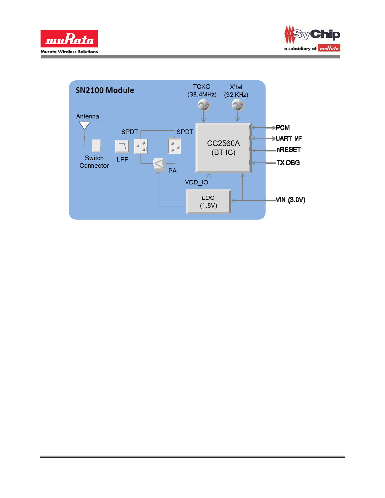
1.3 Block Diagram
Figure 1 SN2100 Module Block Diagram
SyChip/Murata Confidential Page 7 of 31 SN2100 Datasheet Ver. 1.1
Page 8
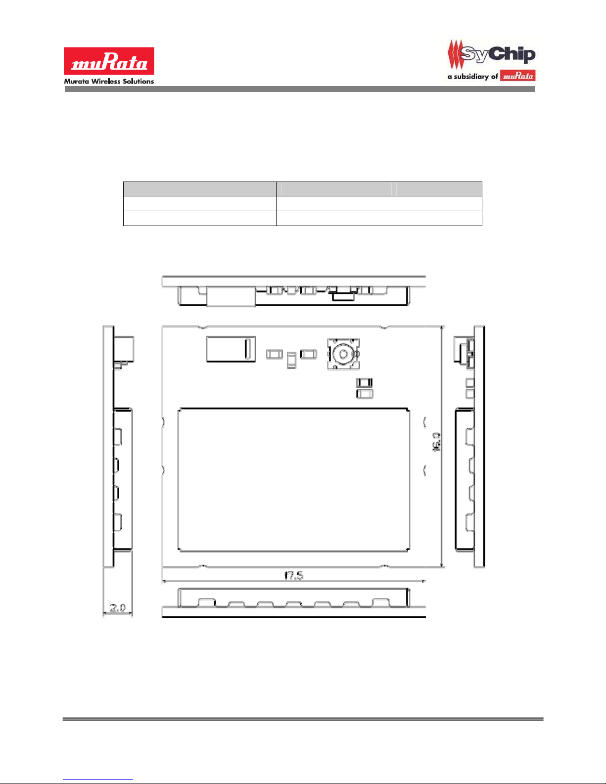
2 Mechanical Specifications
2.1 Module Dimension
Parameter Typical Unit
Dimension (LxWxH) 17.5 x 16.0 x 2.0 mm
Dimension tolerances (LxWxH) +/- 0.2 mm mm
2.2 Module top and side view
SyChip/Murata Confidential Page 8 of 31 SN2100 Datasheet Ver. 1.1
UNIT : mm
Figure 2 Module Top and Side View
Page 9
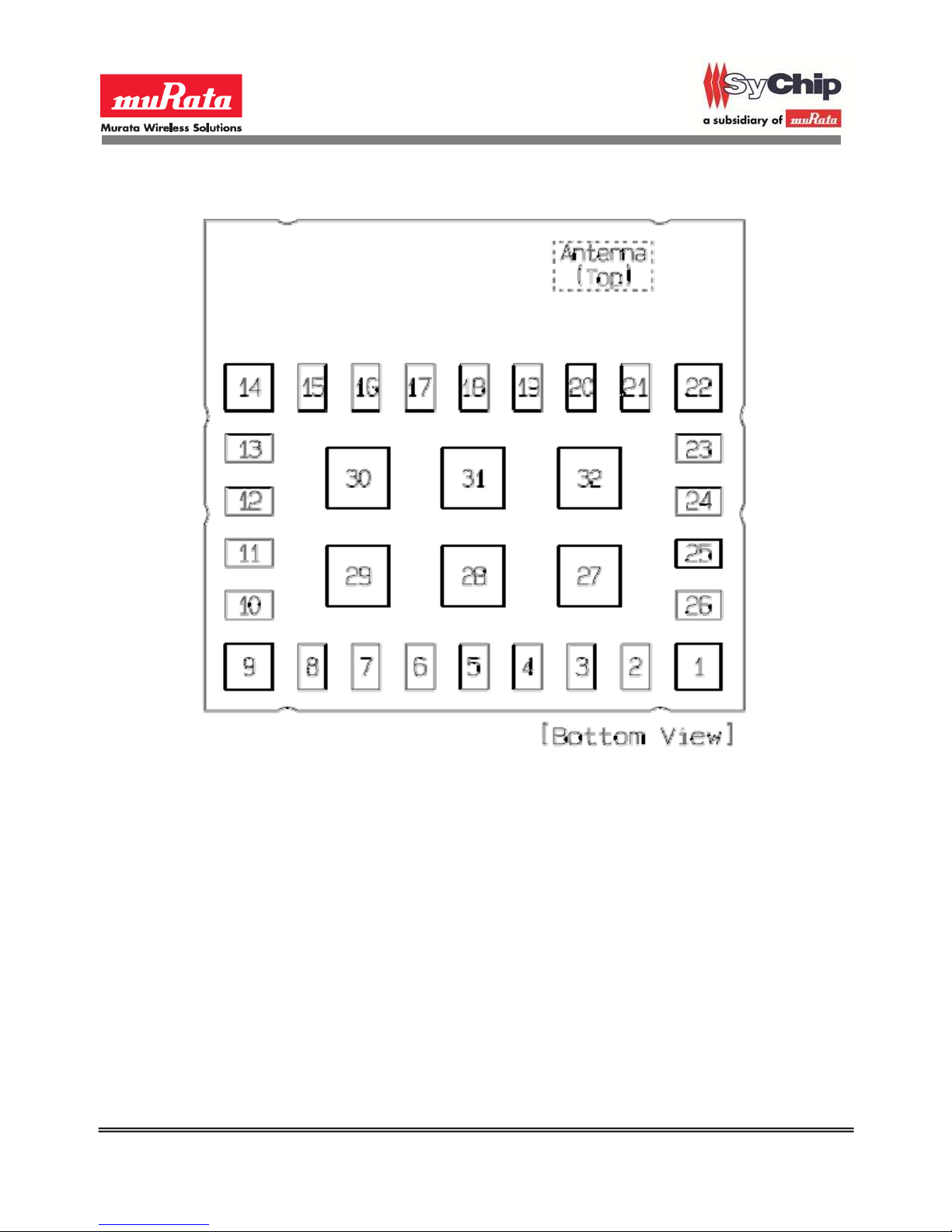
2.3 Module bottom view
Figure 3 Module Bottom View
SyChip/Murata Confidential Page 9 of 31 SN2100 Datasheet Ver. 1.1
Page 10
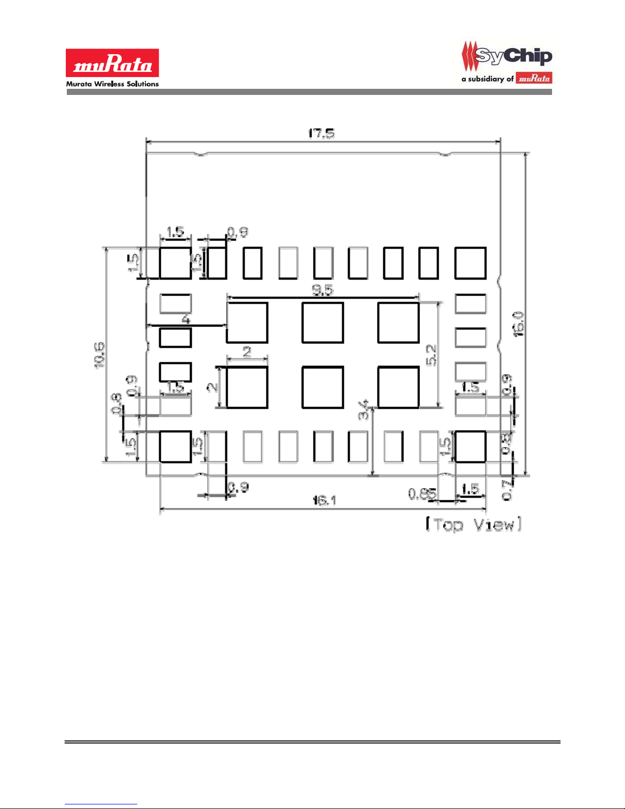
2.4 Detailed mechanical data (top view)
Figure 4 Detailed Mechanical Data (top view)
SyChip/Murata Confidential Page 10 of 31 SN2100 Datasheet Ver. 1.1
Page 11
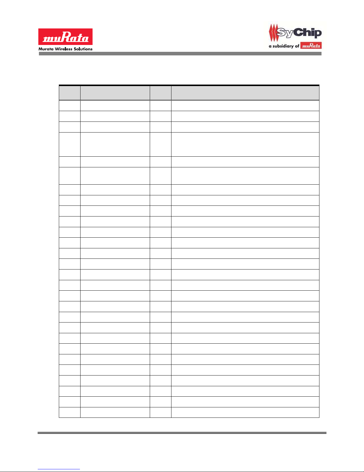
2.5 Module Pin-out
Pin # Pin name I/O Description
1 GND - Ground
2 VIN I Module Power Supply
3 Reserved O Internal for debugging use only
4 HCI_CTS I
5 HCI_TX O HCI UART data transmit
Table 1 Module Connector Signal Description
HCI UART Clear-To-Send.
Module is allowed to send data when HCI_CTS is
low.
6 HCI_RTS O
7 HCI_RX I HCI UART data receive
8 nRESET I Shutdown input (Active Low)
9 GND - Ground
10 AUD_IN I PCM Data Input
11 AUD_OUT O PCM Data Output
12 AUD_CLK I/O PCM Clock
13 AUD_SYNC I/O PCM Frame Sync
14 GND - Ground
15 GND - Ground
16 GND - Ground
17 GND - Ground
18 GND - Ground
19 GND - Ground
20 GND - Ground
21 GND - Ground
HCI UART Request-To-Send
Host is allowed to send data when RTS is low.
22 GND - Ground
23 GND - Ground
24 GND - Ground
25 GND - Ground
26 Reserved - Internal use only
27 GND - Ground
28 GND - Ground
SyChip/Murata Confidential Page 11 of 31 SN2100 Datasheet Ver. 1.1
Page 12
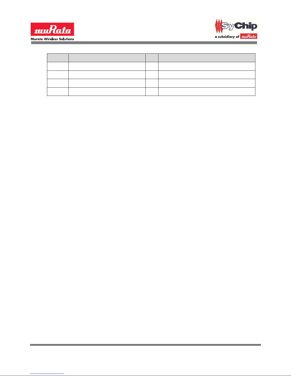
Pin # Pin name I/O Description
29 GND - Ground
30 GND - Ground
31 GND - Ground
32 GND - Ground
SyChip/Murata Confidential Page 12 of 31 SN2100 Datasheet Ver. 1.1
Page 13
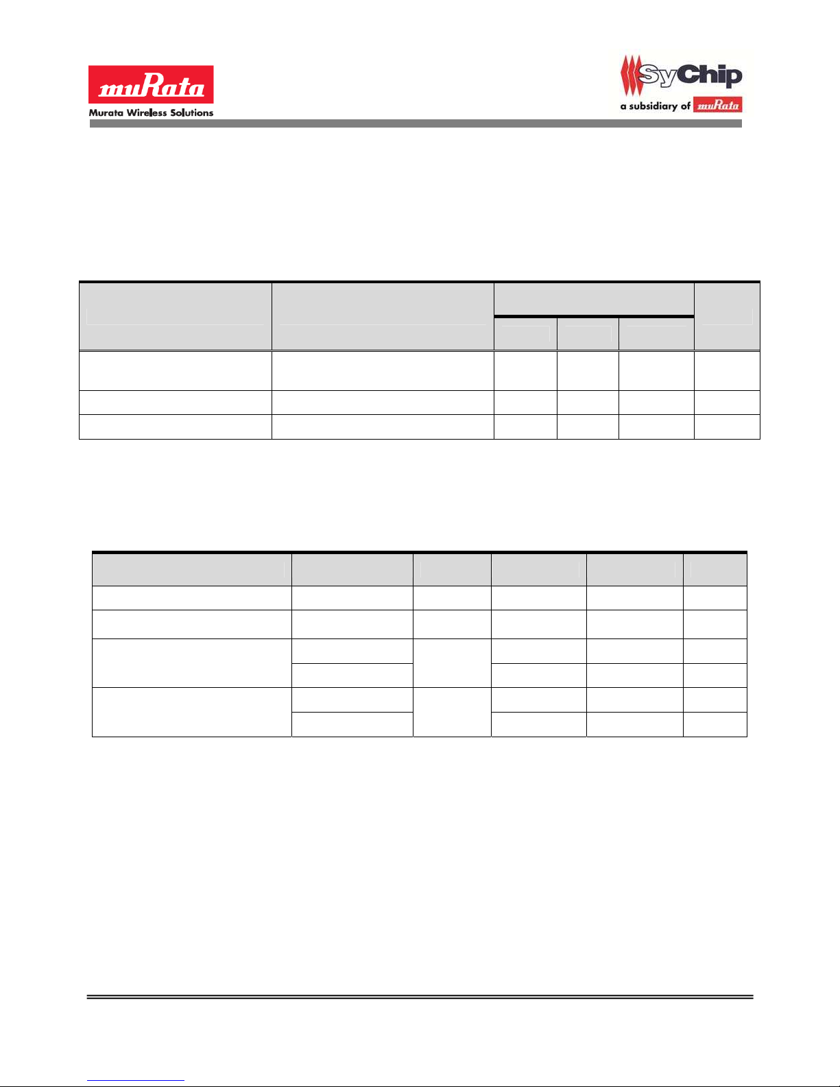
3 DC Electrical Specifications
3.1 Typical Power Consumption
Table 2 Typical Power Consumption
Item Condition
Values
Units
Min Typ Max
Standby mode (after
send script)
TX maximum current VIN = 3.0V, TEMP = 25°C - 165 - mA
RX maximum current VIN = 3.0V, TEMP = 25°C - 50 - mA
VIN = 3.0V, TEMP = 25°C - 3.5 -
mA
3.2 Digital IO Specification
VIN = 3.0V, TEMP = 25°C, unless otherwise stated
Table 3 Digital IO Specification
Item Condition Symbol Min Max UNIT
High Level Input Voltage VIH 0.65 x VDD VDD V
Low Level Input Voltage
At 2/4/8 mA
High Level Output Voltage
At 0.1 mA VDD – 0.2 VDD V
At 2/4/8 mA
Low Level output Voltage
At 0.1 mA 0 0.2 V
VIL
VOH
VOL
0 0.35 x VDD V
0.8 x VDD VDD V
0 0.2 x VDD V
VDD : 1.8V
SyChip/Murata Confidential Page 13 of 31 SN2100 Datasheet Ver. 1.1
Page 14
(1)
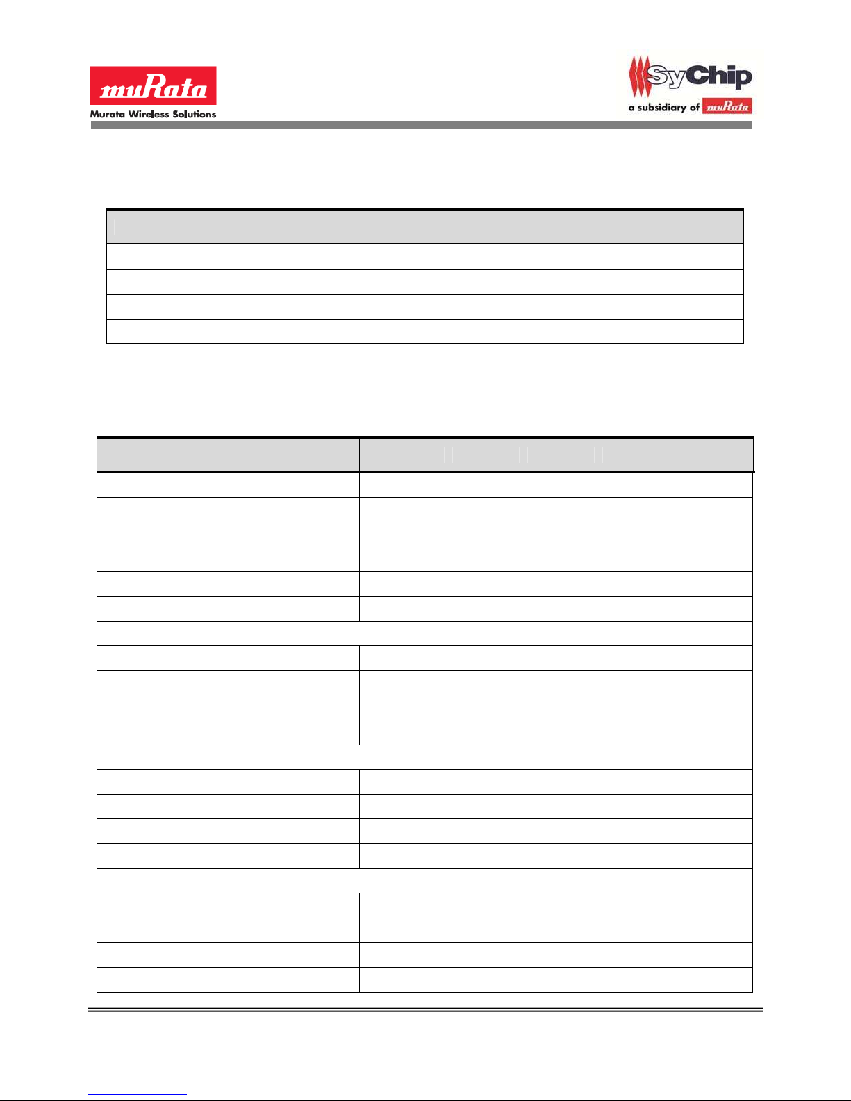
4 RF Specifications
4.1 Bluetooth Specification
Parameter Contents
Bluetooth Specification Ver.2.0
Channel Spacing 1 MHz
The number of channel 79
Power Class 1
4.2 RF Characteristics (TX)
VIN = 3.0V, TEMP = 25°C, at 50 terminal load connected to the RF connector
Table 4 RF Specifications
Parameter Min Typ Max BT Spec Units
Output Power - 18 - 20
Operation Frequency range (RX/TX) 2402 - 2480 - MHz
dBm
-20 dB bandwidth - 0.928 - 1 MHz
Adjacent Channel Power
[M-N] = 2 - -40 - <-20 dBm
[M-N] >= 3 - -43 - <-40 dBm
Modulation Characteristics
Modulation delta f1 avg - 159 -
140< <175
kHz
Modulation delta f2 max - 136 - 115< kHz
Modulation delta f2 avg/delta f1 avg - 0.9 - 0.8< -
Initial Carrier Frequency Tolerance - -2 -
-75< <75
kHz
Carrier Frequency Drift
1 slot -25 2 - -25< <25 kHz
3 slot -40 1 - -40< <40 kHz
5 slot -40 1 - -40< <40 kHz
Maximum drift rate -20 0.5 - -20< <20
kHz/50 us
Out of Band Spurious Emissions
30 – 1000 MHz (Operation Mode) - -50 - <-36 dBm
1000 – 12750 MHz (Operation Mode) - -52 - <-30 dBm
1800 – 1900 MHz (Operation Mode) - -54 - <-47 dBm
5150 – 5300 MHz (Operation Mode) - -54 - <-47 dBm
SyChip/Murata Confidential Page 14 of 31 SN2100 Datasheet Ver. 1.1
Page 15

(1) EIRP.
SyChip/Murata Confidential Page 15 of 31 SN2100 Datasheet Ver. 1.1
Page 16
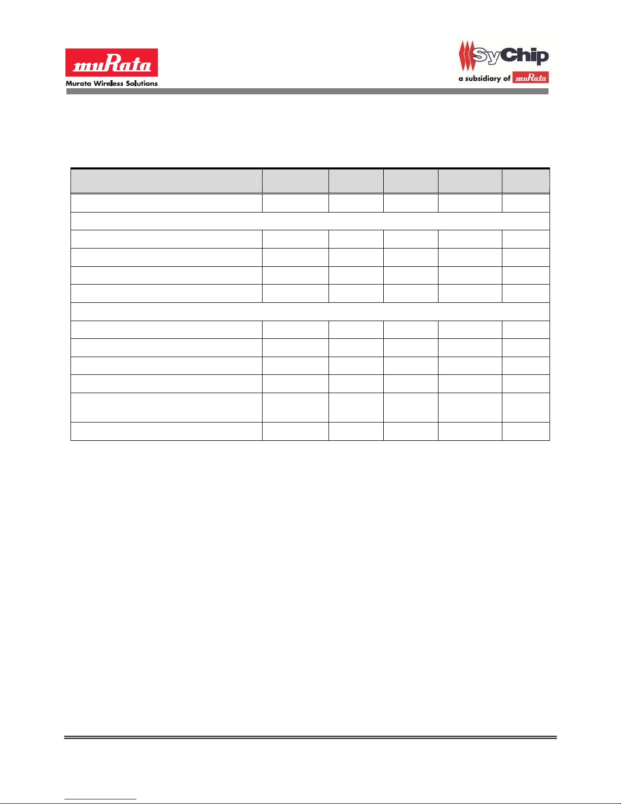
4.3 RF Characteristics (RX)
VIN = 3.0V, TEMP = 25°C, at 50 terminal load connected to the RF connector
Table 5 RF Specifications
Parameter Min Typ Max BT Spec Units
Sensitivity (BER <= 0.1%) - -92 - < -70 dBm
C/I Performance (BER <= 0.1%)
Co-channel ratio (-60 dBm input) - 10 - < 11 dB
1MHz ratio (-60dBm input) - -7 - < 0 dB
2MHz ratio (-60dBm input) - -21 - < -30 dB
3MHz ratio (-67dBm input) - -44 - < -40 dB
Blocking Performance (BER <= 0.1%)
30MHz – 2000MHz -5 - - -10< dBm
2000MHz – 2400MHz -5 - - -27< dBm
2500MHz – 3000MHz -5 - - -27< dBm
3000MHz – 12750MHz -5 - - -10< dBm
Intermodulation Performance
(BER <= 0.1%, -64 dBm input)
Maximum Input Level -4 - - -20< dBm
- -36 - -39< dBm
SyChip/Murata Confidential Page 16 of 31 SN2100 Datasheet Ver. 1.1
Page 17
p
p
5 Environmental Specifications
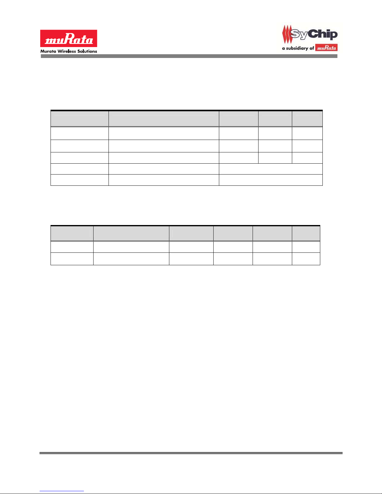
5.1 Absolute maximum ratings
Table 6 Absolute Maximum Rating
Symbol Description Min Max Units
T
o
Tst
VIN Power supply -0.3 5.0 V
MSL Moisture Sensitivity Level 3
RoHS Restriction of Hazardous Substances Compliant
Operating temperature -40 85
Storage temperature -40 85
°C
°C
5.2 Operation conditions
Table 7 Recommended Operating Conditions
Symbol Parameter Min Typ Max Units
VIN Power supply 2.2 3.0 3.3 V
T
o
Operating temperature -40 - 85
°C
SyChip/Murata Confidential Page 17 of 31 SN2100 Datasheet Ver. 1.1
Page 18
6 Application Information
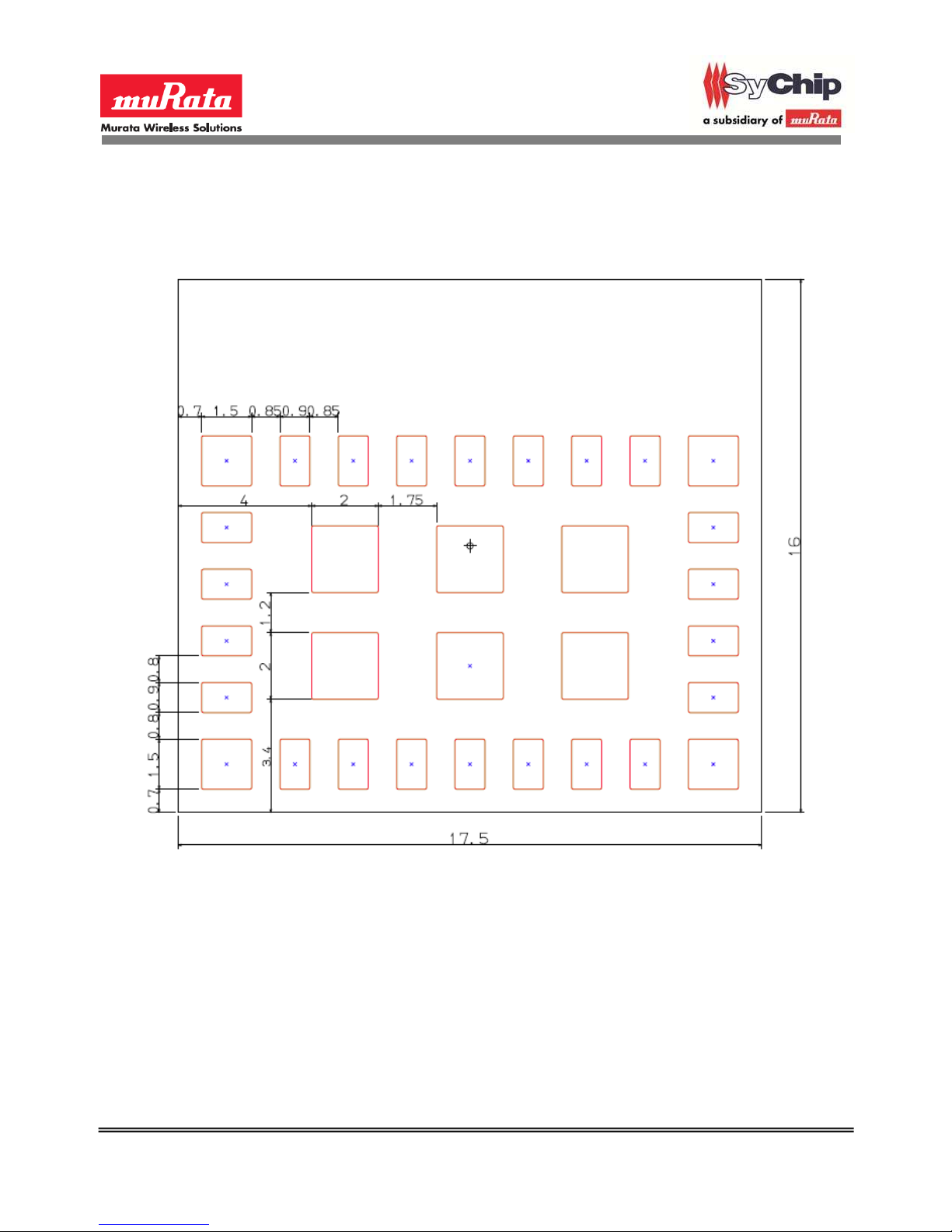
6.1 Recommended host (customer) circuit board PCB pattern
Figure 5 Recommended Host (customer) PCB Pattern
6.2 Host PCB layout recommendations
The SN3020 module has an onboard antenna therefore it requires some special host
PCB layout underneath the module such that the radio can achieve its best RF
performance. Refer to Figure 6 for the requirements.
SyChip/Murata Confidential Page 18 of 31 SN2100 Datasheet Ver. 1.1
Page 19
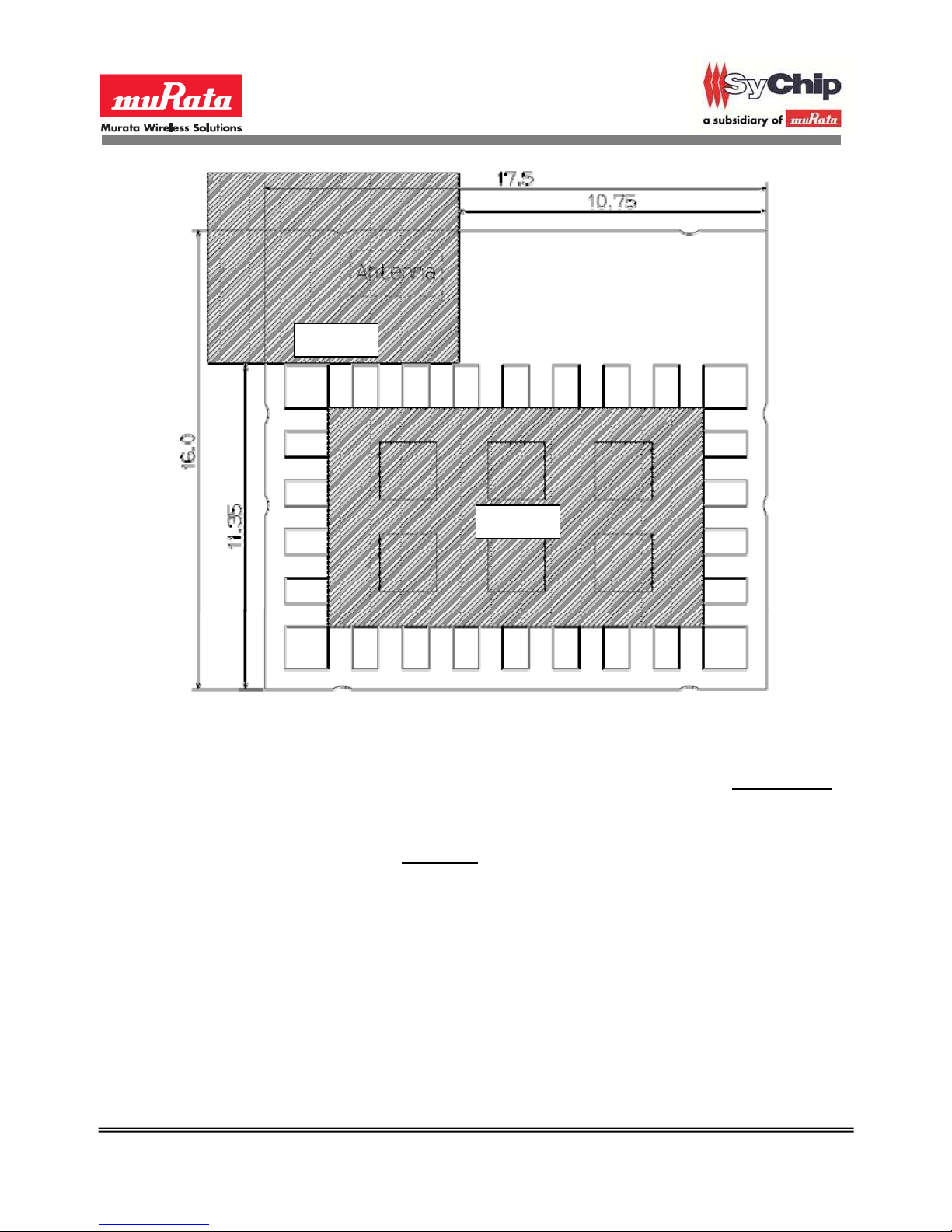
Zone 1
Zone 2
Figure 6 Recommended Host Circuit Board Design underneath the Module
Notes:
1. Due to the surface mount antenna on the module, the area in ‘Zone1’ on all layers of
the customer circuit board should be free of any metal objects. Specifically, there
should be no ground plane, traces, or metal shield case.
2. The area in ‘Zone2’ on the top layer of the customer circuit board should have
ground only with no signal traces.
6.3 Module Location
For optimum EIRP, customer is advised to use the recommended module location on
their respective PCB.
6.3.1 Location in x-y plane
SyChip/Murata Confidential Page 19 of 31 SN2100 Datasheet Ver. 1.1
Page 20
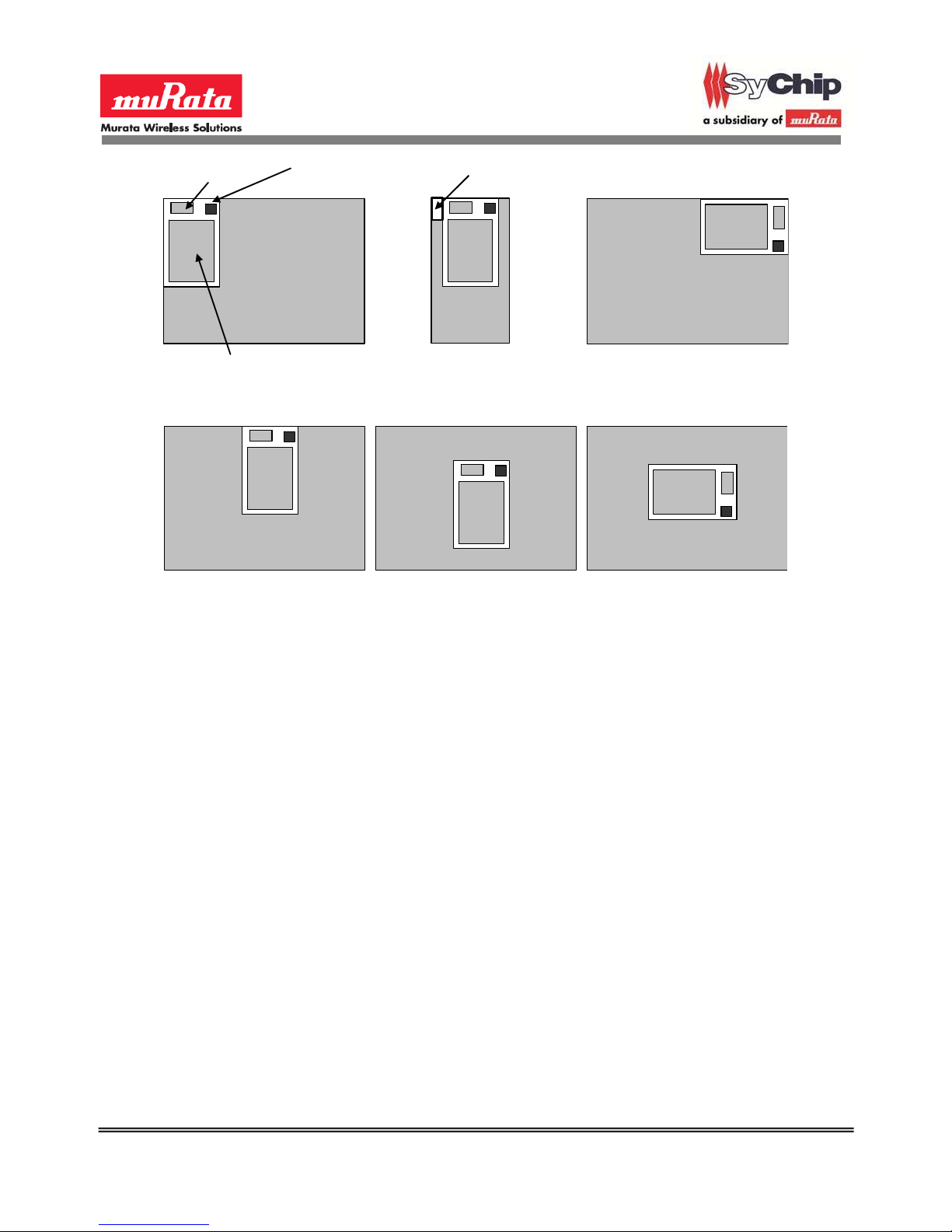
Antenna
Antenna Connector
No GND in this area (See Fig.8)
Shield Case
Figure 7 Recommended Locations in xy-plane
Figure 8 Locations Not Recommended in xy-plane
SyChip/Murata Confidential Page 20 of 31 SN2100 Datasheet Ver. 1.1
Page 21
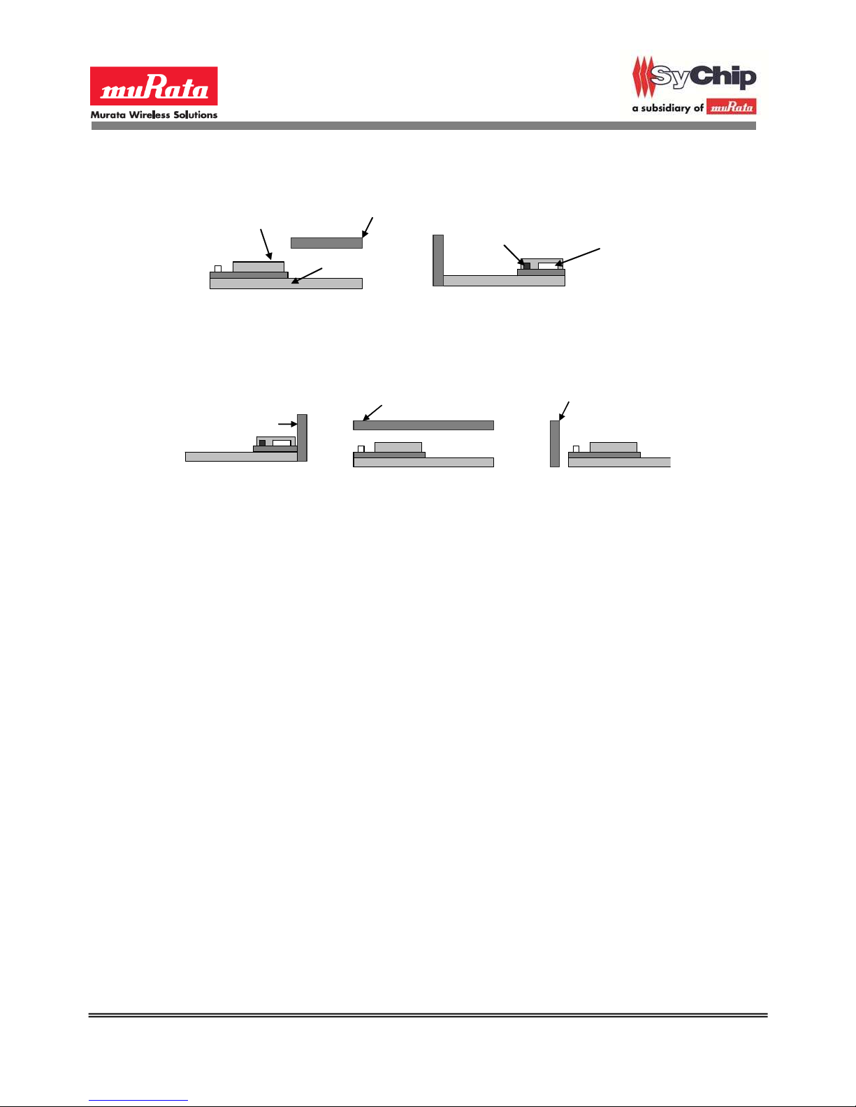
6.3.2 Location in z-plane
Module
Metal
Antenna Connector Antenna
Mother Board
Metal
Figure 9 Recommended Locations in z-plane
Metal
Metal
Metal
Figure 10 Locations Not Recommended in xy-plane
SyChip/Murata Confidential Page 21 of 31 SN2100 Datasheet Ver. 1.1
Page 22
7 Software
7.1 Software Architecture
SN2100 module communicates with host processor via HCI interface. The HCI interface
transports commands, events, ACL, and synchronous data between the device and the
host using HCI data packets.
The Bluetooth profile stack beyond HCI layer is required to be supported from host
processor.
7.2 Bluetooth Profile Stacks
The table below lists the available Bluetooth Profiles and the sources.
Table 8 Bluetooth Stack Availability
Profiles Source Platform
SPP, A2DP
and others
Stonestreet One TI MSP430, TI Stellaris
SyChip/Murata Confidential Page 22 of 31 SN2100 Datasheet Ver. 1.1
Page 23
8 Development Tools
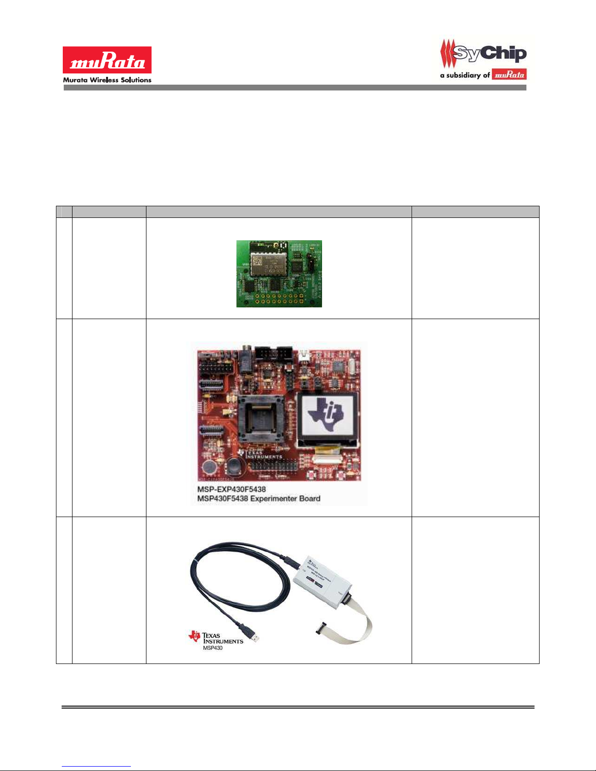
SN2100 EM Development Kit is offered for customer application development on Texas
Instruments MSP430 and Stellaris® platform. The table below lists the related tools that the
customer may need.
Table 9 Development Tools
Tool Description Online Resources
1 88-00150-85 SN2100 EM Development Kit
http://www.murataws.com/2100.htm
2 TI MSP-
EXP430F5438
3 TI MSP-
FET430UIF
MSP430 Experimenter Board
MSP430 USB Debugging Interface
http://www.ti.com/tool/mspexp430f5438
http://www.ti.com/tool/mspfet430uif
SyChip/Murata Confidential Page 23 of 31 SN2100 Datasheet Ver. 1.1
Page 24
9 Assembly Information
9.1 Lead-free soldering reflow profile
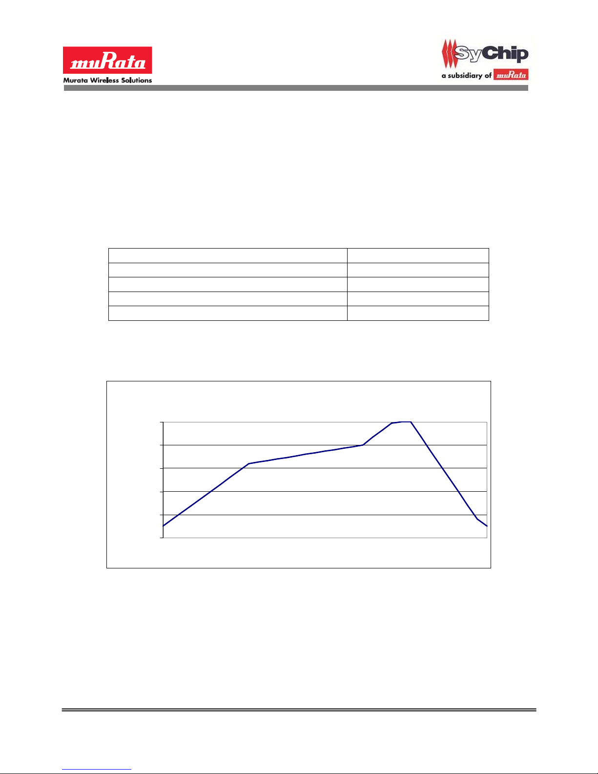
The lead-free solder reflow profile is recommended in the table & graph below. The
profile is used to attach the module to its host PCB.
The module is designed to withstand 2 reflows. Opposite side reflow is prohibited due to
the module weight.
Table 10 Reflow Profile Recommendation
Ramp up rate 3oC/second max
Maximum time maintained above 217oC 120 seconds
Peak temperature 250oC
Maximum time within 5oC of peak temperature 20 seconds
Ramp down rate 6oC/second max
Reflow Prof ile
250
200
150
100
Temperature, C
50
0
Time, seconds
Figure 11 Reflow Profile Pattern
SyChip/Murata Confidential Page 24 of 31 SN2100 Datasheet Ver. 1.1
Page 25
10 Packaging and Marking Information
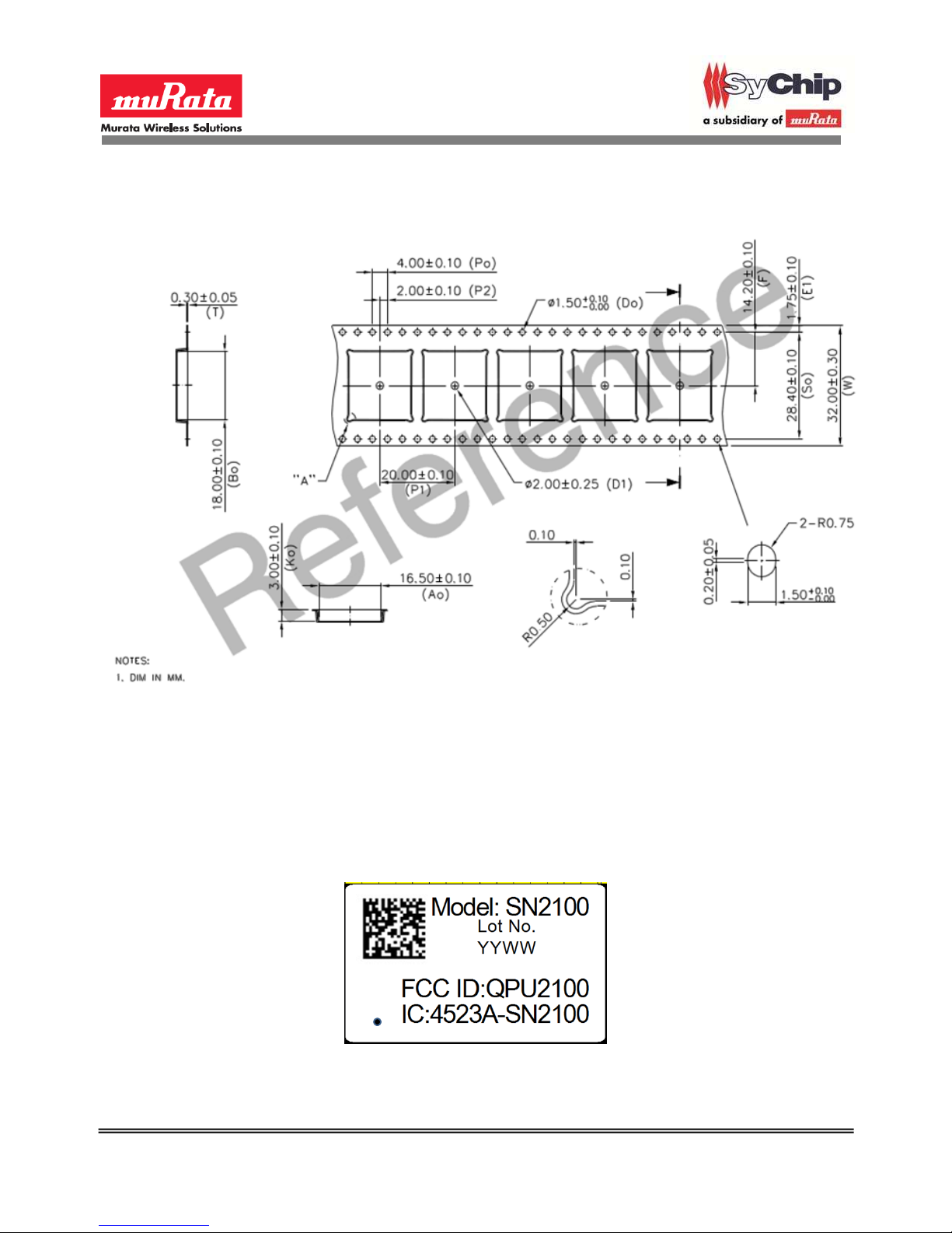
10.1 Carrier Tape Dimensions
Figure 12 Carrier Tape Dimensions
10.2 Module Marking Information
The following marking information may be printed on a permanent label affixed to the
module shield or permanently laser written into the module shield itself. The 2D barcode
is used for internal purposes. A pin 1 ID is stamped into the shield.
Figure 13 Module Marking Detail
SyChip/Murata Confidential Page 25 of 31 SN2100 Datasheet Ver. 1.1
Page 26
11 Ordering Information
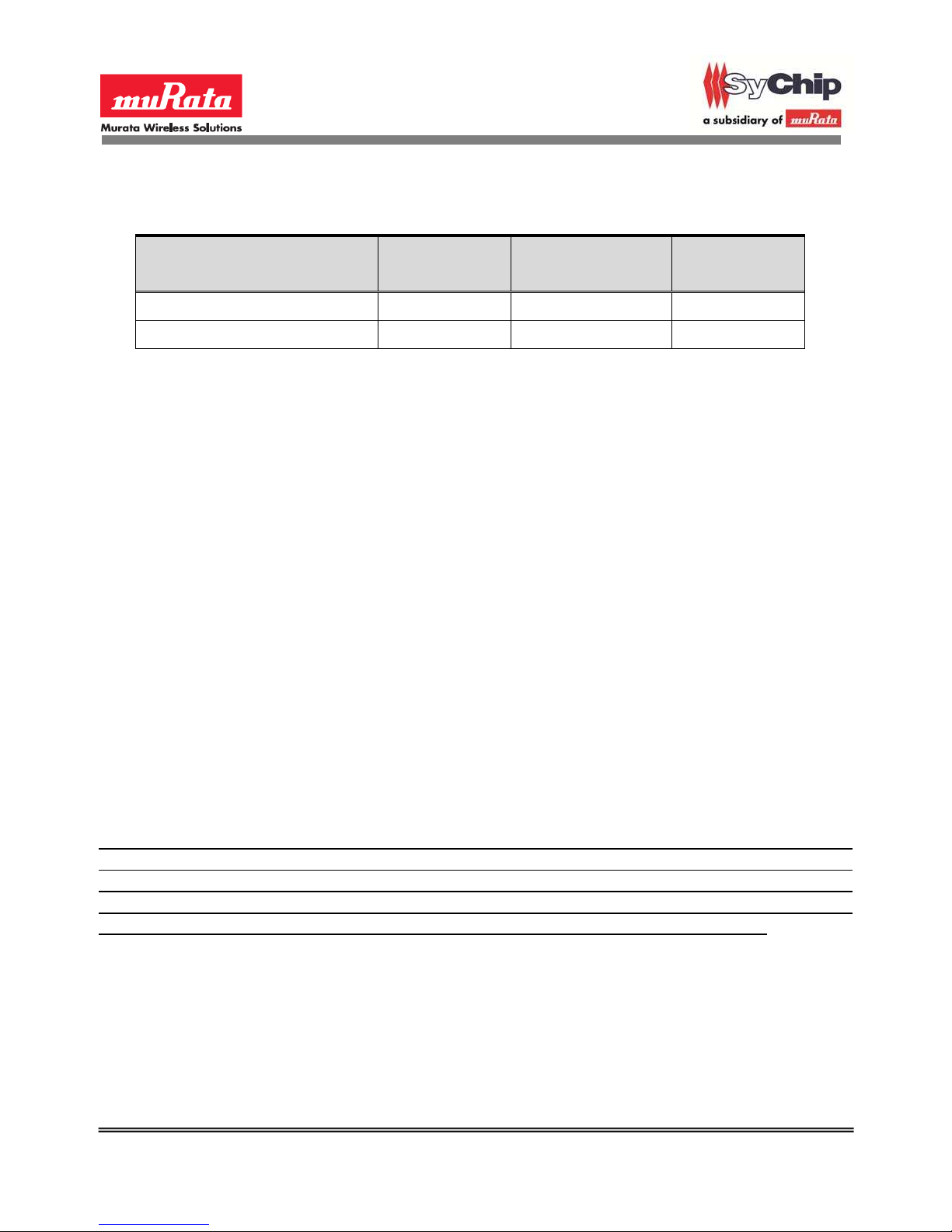
Table 11 Ordering Information
SyChip Model
Product
EM Development Kit SN2100EMK 88-0150-85 1 pc
Module in Tape and Reel SN2100 88-0150-00 500 pcs
Number
SyChip Part
Number
Standard Order
Increment
12 RoHS Declaration
Given supplier declarations, this product does not contain substances that are banned by
Directive 2002/95/EC or contains a maximum concentration of 0.1% by weight in
homogeneous materials for
• Lead and lead compounds
• Mercury and mercury compounds
• Chromium (VI)
• PBB (polybrominated biphenyl)
• PBDE (polybrominated biphenyl ether)
And a maximum concentration of 0.01% by weight in homogeneous materials for
• Cadmium and cadmium compounds
13 Regulatory Information
SN2100 has obtained the certifications described below.
13.1 FCC Notice (USA)
This device using the integrated antenna has been tested to comply with FCC CFR Part
15. The device meets the requirements for modular transmitter approval as detailed in the
FCC public notice DA00.1407. Operation is subject to the following two conditions: (1) this
device may not cause harmful interference, and (2) this device must accept any
interference received, including interference that may cause undesired operation.
The FCC requires the OEM (original equipment manufacturer) to be notified that any
changes or modifications not expressly approved by SyChip, L.L.C may void the user’s
authority to operate the equipment. While an application of the SN2100 module in a
product is not required to obtain a new FCC authorization for the module, this does not
preclude the possibility that some other form of authorization or testing may be required for
that end product.
SyChip/Murata Confidential Page 26 of 31 SN2100 Datasheet Ver. 1.1
Page 27

This equipment has been tested and found to comply with the limits for a Class B digital
device, pursuant to Part 15 of the FCC Rules. These limits are designed to provide
reasonable protection against harmful interference in a residential installation. This
equipment generates uses and can radiate radio frequency energy and, if not installed and
used in accordance with the instructions, may cause harmful interference to radio
communications. However, there is no guarantee that interference will not occur in a
particular installation. If this equipment does cause harmful interference to radio or
television reception, which can be determined by turning the equipment off and on, the user
is encouraged to try to correct the interference by one or more of the following measures:
reorient or relocate the receiving antenna, increase the separation between the equipment
and receiver, connect the equipment into an outlet on a circuit different from that to which
the receiver is connected, or consult the dealer or an experienced radio/TV technician for
help.
13.2 FCC Labeling Requirements
When integrating the SN2100 into a product, the FCC labeling requirements must be met
by the OEM. This includes placing a clearly visible label on the outside of the finished
product specifying the SN2100 FCC identifier (FCC ID:QPU2100) as well as the underlined
FCC Notice above. The exterior label can use wording such as “Contains Transmitter
Module FCC ID:QPU2100” or “Contains FCC ID:QPU2100” although any similar wording
that expresses the same meaning may be used.
13.3 RF Exposure
This module has been certified for remote and base radio applications and is not intended
to be operated within 20cm of the body. If the module will be used for portable applications,
the device must undergo SAR testing.
The following statement must be included as a CAUTION statement in manuals for the
products to alert users on FCC RF exposure compliance:
“WARNING: To satisfy FCC RF exposure requirements for mobile transmitting devices, a
separation distance of 20cm or more should be maintained between the antenna of this
device and persons during operation. To ensure compliance, operations at closer distances
than this are not recommended.”
13.4 IC Notice (Canada)
The term “IC” before the certification/registration number only signifies that the Industry
Canada technical specifications were met.
Le terme “IC” devant le numéro de certification /d’enregistrement signifie seulement que les
spécifications techniques Industrie Canada ont été respectées.
SyChip/Murata Confidential Page 27 of 31 SN2100 Datasheet Ver. 1.1
Page 28

This device complies with Industry Canada license-exempt RSS standard(s). Operation is
subject to the following two conditions: (1) this device may not cause interference, and (2)
this device must accept any interference, including interference that may cause undesired
operation of the device.
Cet appareil est conforme avec Industrie Canada RSS standard exempts de licence (s).
Son utilisation est soumise à Les deux conditions suivantes: (1) cet appareil ne peut pas
provoquer d'interférences et (2) cet appareil doit accepter Toute interférence, y compris les
interférences qui peuvent causer un mauvais fonctionnement du dispositif.
This device complies with Health Canada’s Safety Code 6 / IC RSS-210. The installer of
this device should ensure that RF radiation is not emitted in excess of the Health Canada’s
requirement. Information can be obtained at: http://www.hc-sc.gc.ca/ewh-
semt/pubs/radiation/radio_guide-lignes_direct-eng.php
Cet appareil est conforme avec Santé Canada Code de sécurité 6 / IC RSS-210. Le
programme d'installation de cet appareil doit s'assurer que les rayonnements RF n'est pas
émis au-delà de l'exigence de Santé Canada. Les informations peuvent être obtenues:
http://www.hc-sc.gc.ca/ewh-semt/pubs/radiation/radio_guide-lignes_direct-eng.php
13.5 IC Labeling Requirements
The host device should be properly labeled to identify the module within the host device.
The Industry Canada certification label of a module shall be clearly visible at all times when
installed in the host device, otherwise the host device must be labeled to display the
Industry Canada certification number of the module, preceded by the words “Contains
transmitter module”, or the word “Contains”, or similar wording expressing the same
meaning, as follows:
Contains transmitter module IC:4523A-SN2100,
where 4523A-SN2100 is the module’s certification number.
13.6 CE Notice (Europe)
This device has been tested and certified for use in the European Union.
If this device is used in a product, the OEM has responsibility to verify compliance of the
final product to the EU standards. A Declaration of Conformity must be issued and kept on
file as described in Annex II of the Radio and Telecommunications Terminal Equipment
Directive.
13.7 CE Labeling Requirements
The ‘CE’ mark must be placed on the OEM product per the labeling requirements of the
Directive. Given that the operating frequency band is not harmonized by a few European
countries, the restriction or alert sign must be placed alongside the ‘CE’ mark as shown
below. The restriction is that, if the radio is operated outdoors in the 2450-2483.5 MHz
SyChip/Murata Confidential Page 28 of 31 SN2100 Datasheet Ver. 1.1
Page 29

band, the power must be limited to 10 mW instead of 100 mW. The OEM must account for
this and the product must have the alert mark. It does not require country notifications,
however.
14 Technical Support Contact
SyChip, LLC
2805 Dallas Parkway, Suite 400
Plano, TX 75093
USA
Tel: (972) 202-8900
Fax: (972) 633-0327
Note: SyChip, LLC is an operating unit within Murata Wireless Solutions
15 Disclaimer
Please read this notice before using the SN2100 product.
1. Please note that the only warranty that SyChip LLC (“SyChip”) provides regarding
the products is its conformance to the specifications provided herein. Accordingly, SyChip
shall not be responsible for any defects in products or equipment incorporating such
products, which are caused under the conditions other than those specified in this
specification.
SYCHIP HEREBY DISCLAIMS ALL OTHER WARRANTIES REGARDING THE
PRODUCTS, EXPRESS OR IMPLIED, INCLUDING WITHOUT LIMITATION ANY
WARRANTY OF FITNESS FOR A PARTICULAR PURPOSE, THAT THEY ARE DEFECTFREE, OR AGAINST INFRINGEMENT OF INTELLECTUAL PROPERTY RIGHTS. YOU
AGREE TO INDEMNIFY AND DEFEND SYCHIP AND ITS AFFILIATES AGAINST ALL
CLAIMS, DAMAGES, COSTS AND EXPENSES THAT MAY BE INCURRED, INCLUDING
WITHOUT LIMITATION, ATTORNEY FEES AND COSTS, DUE TO THE USE OF
PRODUCTS.
2. The product is designed and manufactured for general applications, and not for any
particular application, so testing and use of the product shall be conducted at your own risk
and responsibility. Specifically, please observe the following:
i) Please conduct validation and verification of the products in actual
condition of mounting and operating environment before commercial
shipment of the equipment.
SyChip/Murata Confidential Page 29 of 31 SN2100 Datasheet Ver. 1.1
Page 30

ii) Please pay attention to minimize any mechanical vibration or shock, not to
drop the product or a substrate that contains the product during
transportation.
iii) Since the application of static electricity or overvoltage may cause a
defect in the product or deterioration of its reliability, caution must be
taken against exposure to any static electricity generated by electrified
items such as work benches, soldering irons, tools, carrying containers,
etc.
iv) Caution shall be taken to avoid overstress to the product during and after
the soldering process.
v) Since the applied soldering method may deteriorate the reliability,
thorough evaluation is recommended.
vi) In case the product is to be used in equipment or electric circuit that
requires high safety or reliability function or performance, sufficient
reliability evaluation checks for safety shall be performed before
commercial shipment and moreover, due consideration to install a
protective circuit is strongly recommended at customer's design stage.
Please provide an appropriate fail-safe function on your product to prevent
any damages that may be caused by the abnormal function or the failure
of our product.
Notwithstanding the foregoing, the product shall not be used in any application listed below
which requires especially high reliability for the prevention of such defect as may directly
cause damage to the third party's life, body or property.
- Aircraft equipment
- Aerospace equipment
- Undersea equipment
- Power plant control equipment
- Medical equipment
- Transportation equipment (vehicles, trains, ships, etc.)
- Traffic signal equipment
- Disaster prevention / crime prevention equipment
- Application of similar complexity and/or reliability requirements to the applications listed in
the above.
3. SyChip’s warranty as provided in Clause 1 above that the products comply with
descriptions expressly specified in the specifications shall be effective for a period of six (6)
months from the date of delivery. SyChip shall not be liable for any defects that occur in
dry packed products that are installed more than six (6) months after shipment.
SyChip’s liability under this warranty shall be limited to products that are returned during
the warranty period to the address designated by SyChip and that are determined by
SyChip not to conform to such warranty. If SyChip elects to repair or replace such
products, SyChip shall have reasonable time to repair such products or provide
SyChip/Murata Confidential Page 30 of 31 SN2100 Datasheet Ver. 1.1
Page 31

replacements. Repaired products shall be warranted for the remainder of the original
warranty period. Replaced products shall be warranted for a new full warranty period.
For avoidance of doubt, SyChip shall not be liable for any defects that are caused by
neglect, misuse or mistreatment by an entity other than SyChip including improper
installation or testing, or for any products that have been altered or modified in any way by
an entity other than SyChip. Moreover, SyChip shall not be liable for any defects that result
from your or third party’s design, specifications or instructions for such products.
4. Testing and other quality control techniques are used to the extent SyChip deems
necessary. Unless mandated by government requirements, SyChip does not necessarily
test all parameters of each product.
5. End of Life - Please note that we may discontinue the manufacture of products, due
to reasons such as, but not limited to, end of supply of materials and/or components from
our suppliers.
SyChip/Murata Confidential Page 31 of 31 SN2100 Datasheet Ver. 1.1
Page 32

Mouser Electronics
Authorized Distributor
Click to View Pricing, Inventory, Delivery & Lifecycle Information:
Murata:
88-00150-85
 Loading...