

Page 1

Preliminary Specification Number :SP-ZZ1PJ-F
MP Part Number:
LBEE5ZZ1PJ
W-LAN + Bluetooth Module Data Sheet
Qualcomm Chipset
for 802.11a/b/g/n/ac + Bluetooth 4.1 (Dual)
< Specification may be changed by Murata without notice >
Murata(China) Investment Co., Ltd.
Preliminary & Confidential
Page 2

Preliminary Specification Number : SP-ZZ1PJ-F
Revised
Date
Revision
Code
Revised
Page
Revised Item
Change
Reason
April 21,
2017
-
-
-
First release
June 26,
2017
A
3,4
Module Height
Updated
Aug 2,
2017
B
7, 12~20
Absolute Maximum Rating
Operating Condition
DC/RF Characteristics
Updated
Aug 10,
2017
C
22
Reference circuit
Added
Aug 21,
2017
D
21
Land pattern
Added
Nov 2,
2017
E
7, 24~26
Marking
Tape and Reel packing
Added
Dec 25,
2017
F
4, 31~38
Certification information
Appendix
Added
1 / 38
The revision history of the product specification
Preliminary & Confidential
< Specification may be changed by Murata without notice >
Murata(China) Investment Co., Ltd.
Page 3

Preliminary Specification Number : SP-ZZ1PJ-F
2 / 38
TABLE OF CONTENTS
1. SCOPE ..................................................................................................................................................... 3
2. KEY FEATURE ...................................................................................................................................... 3
3. Part Number ........................................................................................................................................... 3
4. RoHS Compliance ................................................................................................................................... 3
5. Block Diagram ........................................................................................................................................ 3
6. Certification Information ....................................................................................................................... 4
6.1. Radio Certification ................................................................................................................... 4
7. DIMENSIONS, MARKING AND TERMINAL CONFIGURATIONS ................................................. 4
7.1. Dimensions ............................................................................................................................... 4
7.2. Pin Layout and PIN Descriptions ........................................................................................... 5
7.3. Marking ..................................................................................................................................... 7
8. ABSOLUTE MAXIMUM RATINGS
9. OPERATING CONDITION
10. External low–power 32.768 kHz clock............................................................................................... 8
11. POWER ON SEQUENCE .................................................................................................................. 9
*2)
11.1. Case 1: 3.3 V power down after 1.8 V .................................................................................. 9
11.2. Case 2: 1.8 V power down after 3.3 V ................................................................................ 10
11.3. Case 3: All power rails supplied with 3.3 V .......................................................................11
12. Digital I/O Requirements ................................................................................................................. 12
13. INTERFACE TIMING AND AC CHARACTERISTICS ................................................................. 12
13.1. Bluetooth UART Timing .................................................................................................... 12
13.2. I2S Timing ........................................................................................................................... 12
13.3. SDIO Timing ....................................................................................................................... 12
14. DC / RF Characteristics.................................................................................................................... 13
14.1. DC/RF Characteristics for IEEE802.11b - 2.4GHz .......................................................... 13
14.2. DC/RF Characteristics for IEEE802.11g - 2.4GHz .......................................................... 14
14.3. DC/RF Characteristics for IEEE802.11n – 2.4GHz ......................................................... 15
14.4. DC/RF Characteristics for IEEE802.11ac – 2.4GHz ........................................................ 16
14.5. DC/RF Characteristics for IEEE802.11a - 5GHz ............................................................. 17
14.6. DC/RF Characteristics for IEEE802.11n - 5GHz ............................................................. 18
14.7. DC/RF Characteristics for IEEE802.11ac - 5GHz ............................................................ 19
14.8. DC/RF Characteristics for Bluetooth ................................................................................ 20
14.9. DC/RF Characteristics for Bluetooth (LE) ........................................................................ 21
15. LAND PATTERN (TOP VIEW) ........................................................................................................ 22
16. REFERENCE CIRCUIT ................................................................................................................... 23
17. TAPE AND REEL PACKING ........................................................................................................... 24
18. NOTICE ............................................................................................................................................. 27
18.1. Storage Conditions: ............................................................................................................ 27
18.2. Handling Conditions: ......................................................................................................... 27
18.3. Standard PCB Design (Land Pattern and Dimensions): ................................................. 27
18.4. Notice for Chip Placer: ....................................................................................................... 27
18.5. Soldering Conditions: ......................................................................................................... 28
18.6. Cleaning: ............................................................................................................................. 28
18.7. Operational Environment Conditions: .............................................................................. 28
18.8. Input Power Capacity: ........................................................................................................ 29
19. PRECONDITION TO USE OUR PRODUCTS ............................................................................... 30
Please be aware that an important notice concerning availability, standard warranty and use in critical applications of
Murata products and disclaimers thereto appears at the end of this specification sheet.
*1)
................................................................................................... 8
................................................................................................................ 8
Preliminary & Confidential
< Specification may be changed by Murata without notice >
Murata(China) Investment Co., Ltd.
Page 4
Preliminary Specification Number : SP-ZZ1PJ-F
Ordering Part Number
Description
LBEE5ZZ1PJ
MP order
LBEE5ZZ1PJ-TEMP
In case of sample order
1. SCOPE
This specification is applied to the IEEE802.11a/b/g/n/ac W-LAN + Bluetooth 4.1 combo module.
2. KEY FEATURE
- Chipset : QCA9377-3
- Size : 7.2 x 7.4 x 1.25 (max) mm
- PCB w/ shielded resin mold module
- IEEE802.11a/b/g/n/ac dual band 2.4G/5G
- Supports BT4.1
- SDIO 3.0 (WLAN), UART/PCM (Bluetooth)
- Lead Free Module
3. Part Number
4. RoHS Compliance
This module is compliant with the RoHS directive.
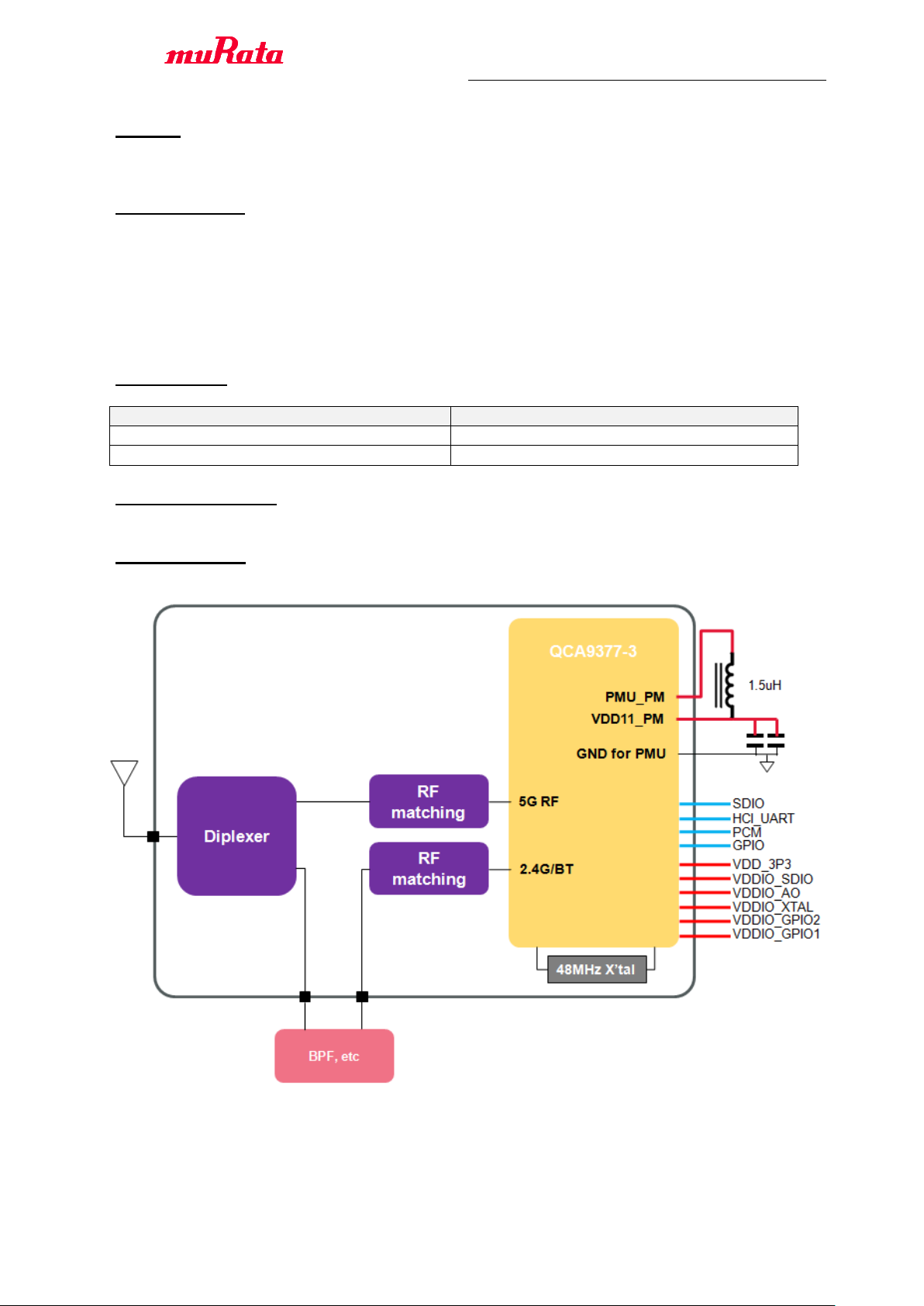
5. Block Diagram
3 / 38
Preliminary & Confidential
< Specification may be changed by Murata without notice >
Murata(China) Investment Co., Ltd.
Page 5
Preliminary Specification Number : SP-ZZ1PJ-F
FCC ID
VPYLB1PJ
IC
772C-LB1PJ
Mark
Dimension
Mark
Dimension
Mark
Dimension
L
7.40±0.20
W
7.20±0.20
T
1.25 max
a1
0.30±0.10
a2
0.30±0.10
a3
0.30±0.10
a4
0.80±0.10
a5
0.30±0.10
b1
0.20±0.15
b2
0.25±0.15
b3
1.45±0.15
b4
5.15±0.15
b5
0.20±0.15
b6
1.05±0.15
b7
1.35±0.15
b8
1.55±0.15
c1
0.55±0.10
c2
0.55±0.10
c3
0.55±0.10
c4
0.80±0.10
c5
0.30±0.10
e1
0.30±0.10
e2
0.30±0.10
e3
0.30±0.10
e4
0.30±0.10
e5
0.30±0.10
6. Certification Information
6.1. Radio Certification
USA/Canada
*Please follow installation manual in Appendix
Europe
EN300328 v2.1.1, EN301893 v2.1.1 and EN300440 v2.1.1 test reports are prepared.
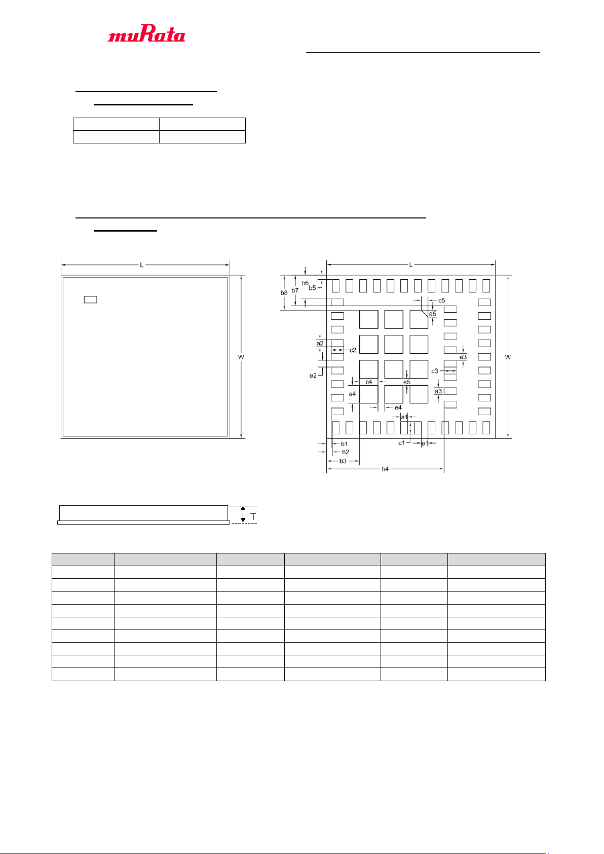
7. DIMENSIONS, MARKING AND TERMINAL CONFIGURATIONS
7.1. Dimensions
<TOP VIEW> <BOTTOM VIEW>
4 / 38
<SIDE VIEW>
Table 1 Dimension (Unit: mm)
(unit : mm)
Preliminary & Confidential
< Specification may be changed by Murata without notice >
Murata(China) Investment Co., Ltd.
Page 6
Preliminary Specification Number : SP-ZZ1PJ-F
Pin
NO.
Terminal Name
Type
VDDIO or
pad voltage
Connection to
IC terminal
Description
1
GND
Ground
- - Ground
2
VBUCK_GND_PM
Ground
-
VBUCK_GND_PM
Ground for internal 1.1 V regulator
3
PWM_PM
O
1.1V
PWM_PM
SWREG PMU 1.1V output.
4
VDD11_PM
I
1.1V
VDD11_PM
1.1 V voltage feedback to SWREG PMU.
5
GND
Ground
- - Ground
6
SDIO_DATA3
I/O
VDDIO_SDIO
SDIO_D3
SDIO data bus D3
7
SDIO_DATA2
I/O
VDDIO_SDIO
SDIO_D2
SDIO data bus D2
8
SDIO_DATA1
I/O
VDDIO_SDIO
SDIO_D1
SDIO data bus D1
9
SDIO_DATA0
I/O
VDDIO_SDIO
SDIO_D0
SDIO data bus D0
10
SDIO_CMD
I
VDDIO_SDIO
SDIO_CMD
SDIO CMD line signal
11
SDIO_CLK
OD
(1)
VDDIO_SDIO
SDIO_CLK
SDIO clock signal
12
VDDIO_SDIO
Power
1.8V or 3.3V
VDDIO_SDIO
Voltage supply for SDIO
13
SDIO_INTERRUPT_L
O
VDDIO_SDIO
SDIO_INTERRUPT_L
SDIO interrupt signal
14
GND
Ground
- - Ground
15
32KHz_CLK_IN
I
VDDIO_GPIO2
LF_CLK_IN
External low–power 32.768 kHz clock input
16
VDDIO_GPIO2
Power
1.8V or 3.3V
VDDIO_GPIO2
Voltage supply
17
HCI_UART_WAKEHOST
OD
(1)
VDDIO_GPIO2
HCI_UART_WAKEHOST
Bluetooth wakeup host. Active high
18
WLAN_RF_KILL_L
I
VDDIO_GPIO2
WLAN_RFKILL_L
Turn off WLAN RF analog and front–end.
Active low.
19
GND
Ground
- - Ground
20
2G_WIFI/BT_RF_OUT
A,O - -
2G WIFI and BT output
21
GND
Ground
- - Ground
22
2G_WIFI/BT_RF_IN
A, I - -
2G WIFI and BT input
23
GND
Ground
- - Ground
24
ANT
A, I/O
- - RF Transmit / Receive Antenna
25
GND
Ground
- - Ground
Top View
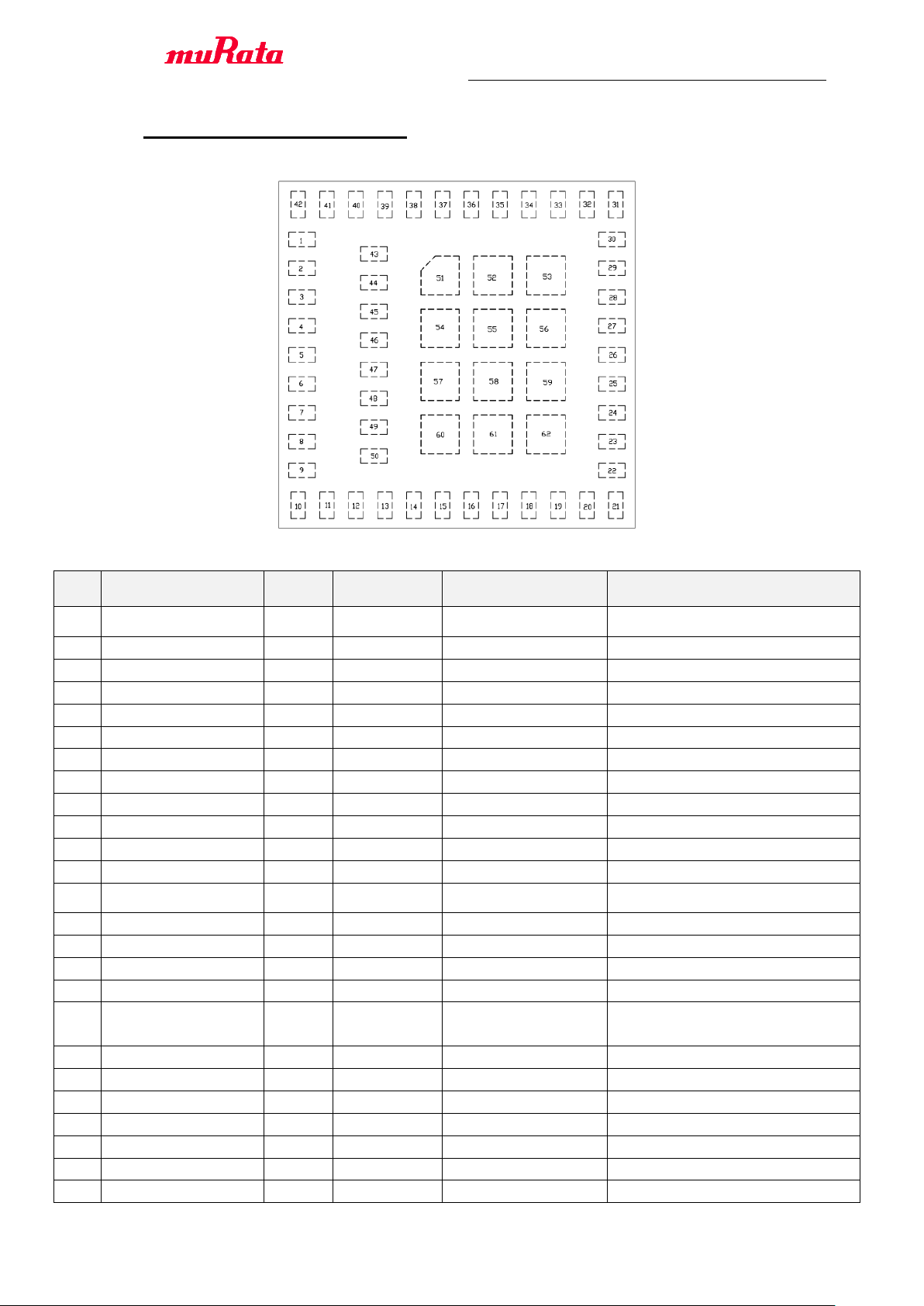
7.2. Pin Layout and PIN Descriptions
5 / 38
Table 2 Terminal Configurations
Preliminary & Confidential
< Specification may be changed by Murata without notice >
Murata(China) Investment Co., Ltd.
Page 7

Preliminary Specification Number : SP-ZZ1PJ-F
26
3D_FRAME_SYNC
I
VDDIO_GPIO1
3D_FRAME_SYNC
Frame sync signal from TV to sync with 3D
glass via Bluetooth.
27
HCI_UART_RXD
I
VDDIO_GPIO1
HCI_UART_RXD
UART RXD signal
28
HCI_UART_TXD
O
VDDIO_GPIO1
HCI_UART_TXD
UART TXD signal
29
HCI_UART_RTS
O
VDDIO_GPIO1
HCI_UART_RTS
UART RTS signal
30
HCI_UART_CTS
I
VDDIO_GPIO1
HCI_UART_CTS
UART CTS signal
31
PCM_CLK
I
VDDIO_GPIO1
BT_I2S_SCK
Bluetooth PCM_CLK signal
32
PCM_SYNC
I/O
VDDIO_GPIO1
BT_I2S_WS
Bluetooth PCM_SYNC signal
33
PCM_IN
OD
(1)
VDDIO_GPIO1
BT_I2S_SDI
Bluetooth PCM_IN signal
34
PCM_OUT
O
VDDIO_GPIO1
BT_I2S_SDO
Bluetooth PCM_OUT signal
35
GND
Ground
- - Ground
36
VDDIO_XTAL
Power
1.8V or 3.3V
VDDIO_XTAL
Voltage supply for XTAL
37
VDDIO_GPIO1
Power
1.8V or 3.3V
VDDIO_GPIO1
Voltage supply
38
GND
Ground
- - Ground
39
WLAN_EN
I
VDDIO_AO
WL_EN
WLAN enable. Active high
40
BT_EN
I
VDDIO_AO
BT_EN
Bluetooth enable. Active high
41
VDD_3P3
Power
3.3V
VDD33_PM
3.3 V input voltage
42
VDDIO_AO
Power
1.8V or 3.3V
VDDIO_AO_PM
Always–on I/O supply for power
management and real–time clock. This
supply must be present if any other supply
is present.
43
GND
Ground
- - Ground
44
LTE_UART_RXD
I
VDDIO_GPIO1
LTE_UART_RXD
LTE coexistence signal.
LTE_UART_RXD or LTE_FS.
45
LTE_UART_TXD
O
VDDIO_GPIO1
LTE_UART_TXD
LTE co– existence signal.
LTE_UART_TXD or LTE_PRI.
46
CLK_REQ
O
VDDIO_GPIO1
CLK_REQ
Clock request output
47
DBG_UART_TXD
OD
(1)
VDDIO_AO
GPIO[19]
DBG_UART_TXD
48
DBG_UART_RXD
OD
(1)
VDDIO_GPIO2
GPIO[18]
DBG_UART_RXD
49
QOW
OD
(1)
VDDIO_GPIO2
QOW
This signal can be used to enable for
external Wireless charging UART circuit.
50~
62
GND
Ground
- - Ground
6 / 38
(1) OD means this PIN is a digital output signal with open drain, an external pull-up or pull-down resistor is needed when this PIN is
used.
Preliminary & Confidential
< Specification may be changed by Murata without notice >
Murata(China) Investment Co., Ltd.
Page 8
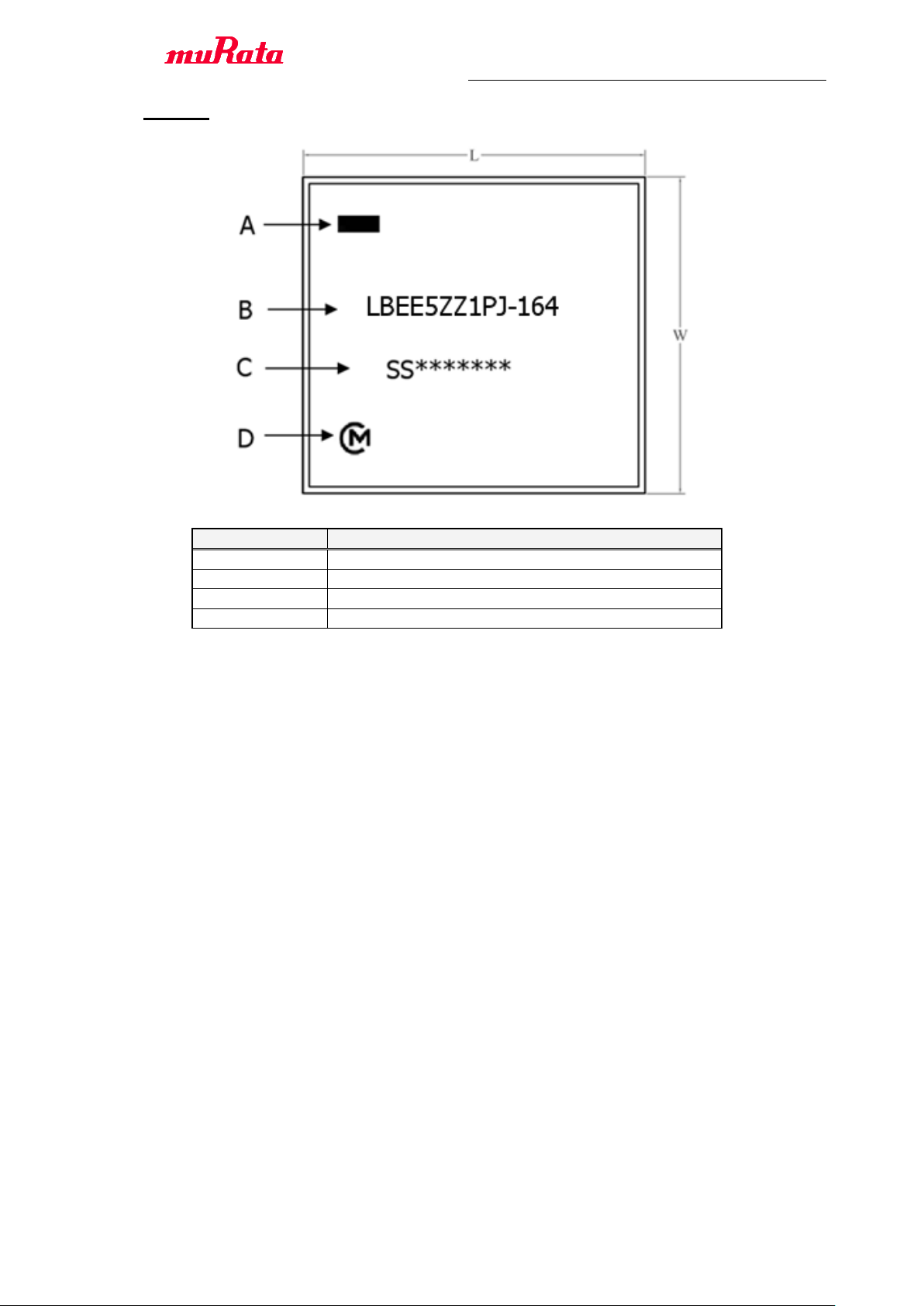
7.3. Marking
Marking
Meaning
A
Pin 1 Marking
B
Inspection Number
C
Module P/N
D
Murata Logo
Preliminary Specification Number : SP-ZZ1PJ-F
7 / 38
Preliminary & Confidential
< Specification may be changed by Murata without notice >
Murata(China) Investment Co., Ltd.
Page 9
Preliminary Specification Number : SP-ZZ1PJ-F
Parameter
min.
max.
Unit
Storage Temperature
TBD
TBD
deg.C
Supply Voltage
VDD_3P3
-0.3
3.65
V
VDDIO_SDIO
VDDIO_GPIO1
VDDIO_GPIO2
VDDIO_XTAL
VDDIO_AO
-0.3
3.6
V
Parameter
min.
typ.
max.
unit
Operating Temperature
-40 - 85
deg.C
Specification Temperature range
TBD
TBD
TBD
deg.C
Supply Voltage
VDD_3P3
3.135
3.3
3.465
V
VDDIO_SDIO
VDDIO_GPIO1
VDDIO_GPIO2
VDDIO_XTAL
VDDIO_AO
1.71
1.8 or 3.3
3.46
V
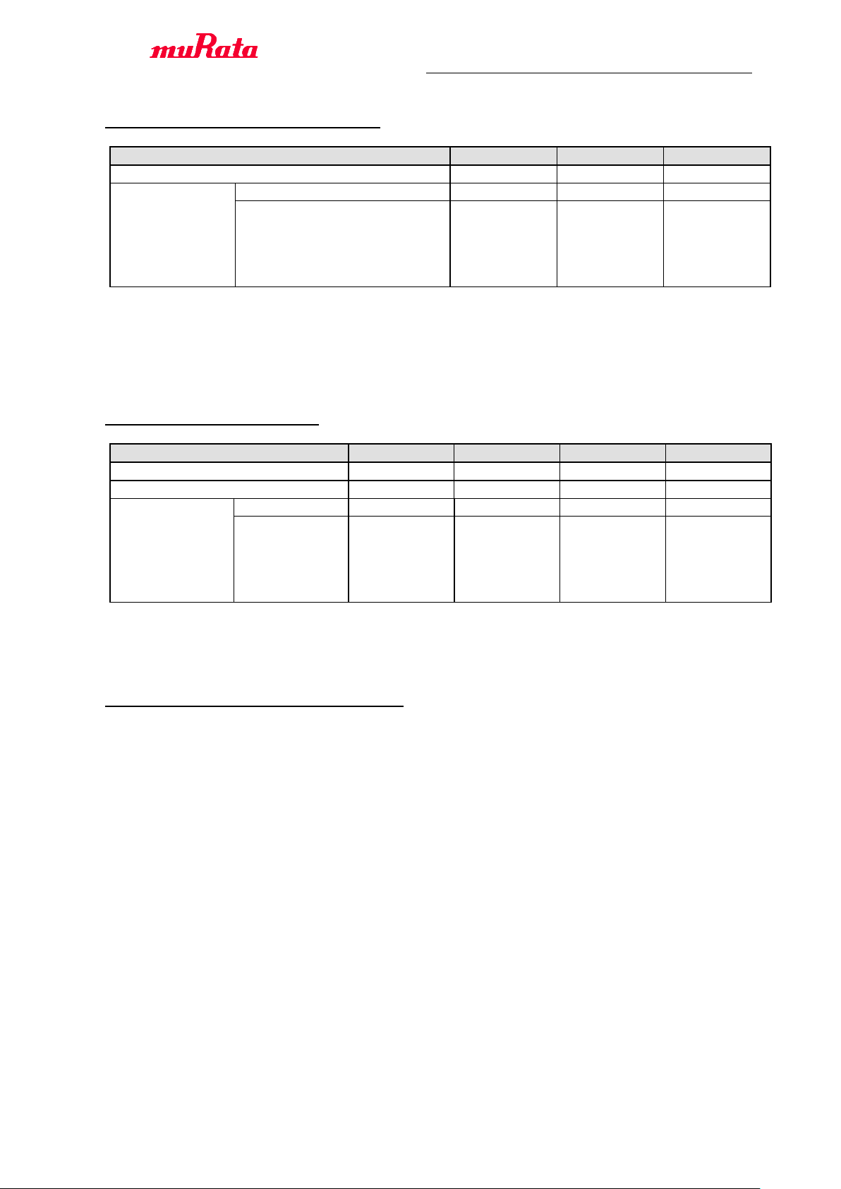
8. ABSOLUTE MAXIMUM RATINGS
*1)
*1)
Stresses in excess of the absolute ratings may cause permanent damage. Functional operation
is not implied under these conditions. Exposure to absolute ratings for extended periods of time
may adversely affect reliability. No damage assuming only one parameter is set at limit at a time
with all other parameters are set within operating condition.
9. OPERATING CONDITION
*2)
8 / 38
*2)
Functionality is guaranteed but the specifications require the derating at over-temperatures,
over-voltage condition.
10. External low–power 32.768 kHz clock
TBD
Preliminary & Confidential
< Specification may be changed by Murata without notice >
Murata(China) Investment Co., Ltd.
Page 10
Preliminary Specification Number : SP-ZZ1PJ-F
Symbol
Parameter
Min
Max
Units
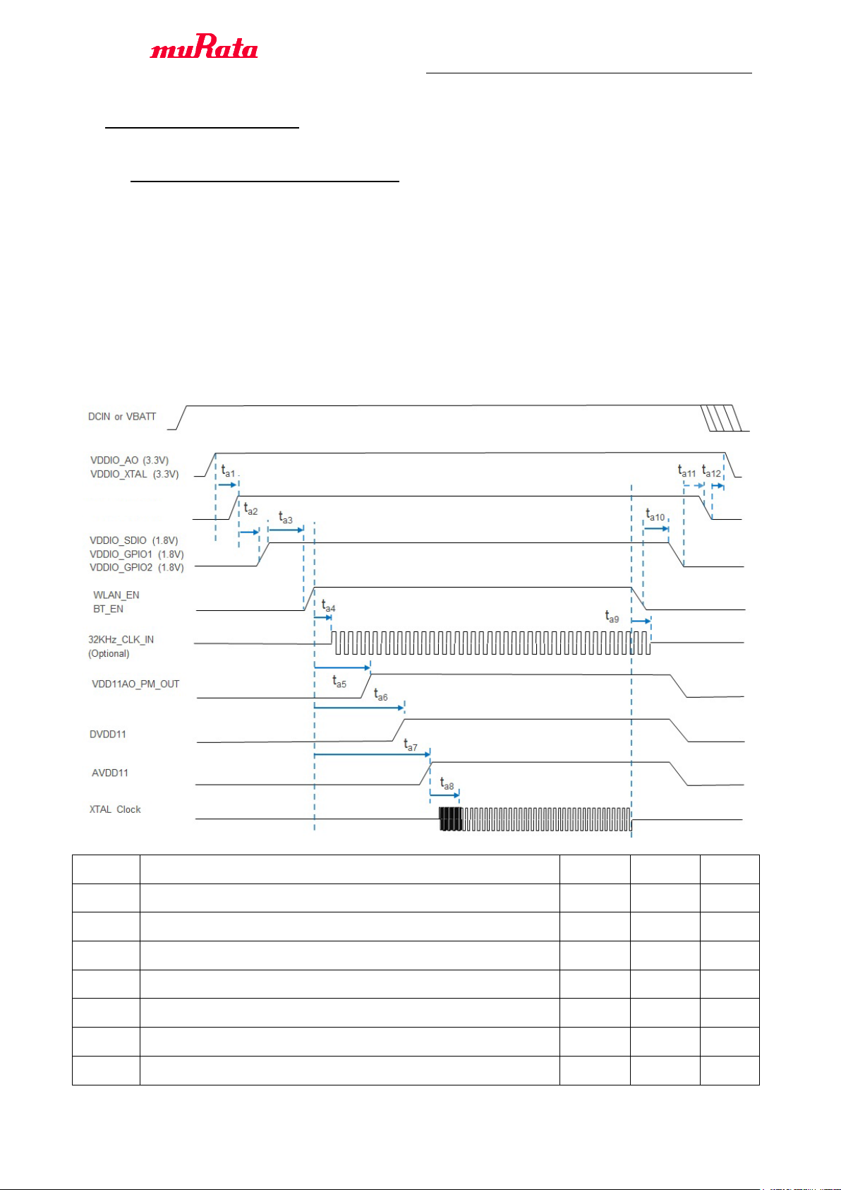
ta1
No requirement if VDDIO_AO connected to 3.3 V
0 - μs
ta2
90% of 3.3 V to 10% of 1.8 V
0 0 μs
ta3
90% of VDDIO_GPIO to 0.7 V of both WLAN_EN and BT_EN
10 - μs
ta4
WLAN_EN valid to LF_CLK_IN input
0 - μs
ta5
WLAN_EN valid to VDD11AO_PM_OUT established
-
50
μs
ta6
WLAN_EN to DVDD11
-
3.5
ms
ta7
WLAN_EN to AVDD11
- 4 ms
VDD_3.3 (3.3V)
11. POWER ON SEQUENCE
11.1. Case 1: 3.3 V power down after 1.8 V
If the battery source can be removed from the end user device (battery removed, AC/DC plugged
in), this is the recommended power sequence. It will avoid violating the power off sequence by
allowing the 3.3 V rail to shut down after the 1.8 V rail.
Notes:
1. VDDIO_GPIO voltage should match VIO voltage from the host. In some applications,
VDDIO_GPIO may connected to 3.3 V upon Host VIO voltage.
2. In this case, both WLAN_EN and BT_EN on the 1PJ are at 3.3 V due to using the VDD_AO
power rail. If the host VIO voltage is 1.8 V, it must have level shifters to interface with host.
3. All host interface signals must stay floating or low before valid power on sequence (WLAN_EN
and BT-EN goes high).
9 / 38
Preliminary & Confidential
< Specification may be changed by Murata without notice >
Murata(China) Investment Co., Ltd.
Page 11
Preliminary Specification Number : SP-ZZ1PJ-F
ta8
AVDD11 to XTAL clock stable
1 - ms
ta9
WLAN_EN de-assert (“low”) to LF_CLK_IN de-assert
(tristate or low)
0 - μs
t
a10
Both WLAN_EN = low and BT_EN = low to 90% of 1.8 V
10 - μs
t
a11
3.3 V always higher than 1.8 V during operation, with power
off by removing battery or unplugging AC/DC
0 - μs
t
a12
VDDIO_AO and VDDIO_XTAL should be connected to 3.3 V
power rail
0 - μs
Symbol
Parameter
Min
Max
Units
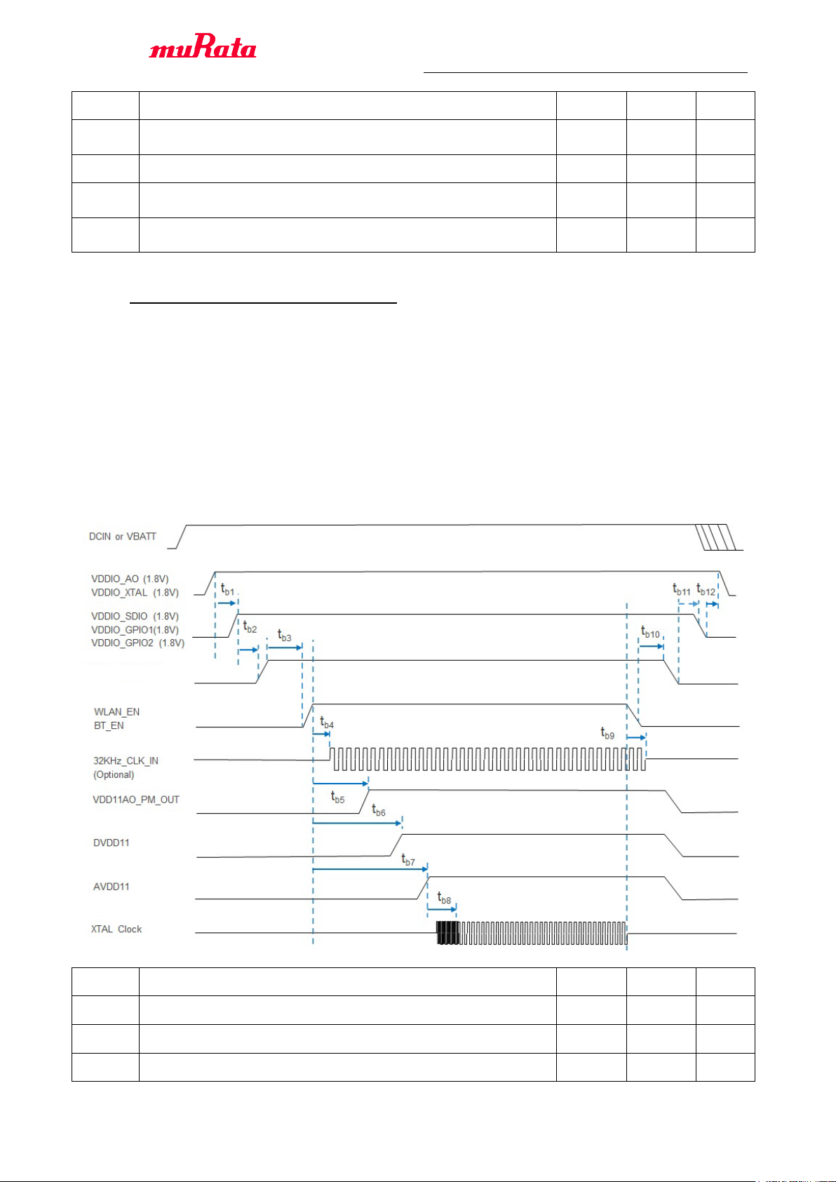
tb1
No requirement if VDDIO_AO connected to 1.8 V
0 - μs
tb2
90% of 1.8 V to 10% of 3.3 V
0 - μs
tb3
90% of 3.3 V to 0.7 V of both WLAN_EN and BT_EN
10 - μs
VDD_3.3 (3.3V)
11.2. Case 2: 1.8 V power down after 3.3 V
If the battery source cannot be removed from the end user device, this is the recommended
power sequence for this application. This sequence allows the software to control the power
on/off sequence.
Notes:
1. VDDIO_GPIO voltage should match VIO voltage from the host. In some applications,
VDDIO_GPIO may connected to 3.3 V upon host VIO voltage.
2. Both WLAN_EN and BT_EN of 1PJ are 1.8 V. If host VIO voltage is 1.8 V, it does
not need level shifter to interface with host.
3. All host interface signals must stay floating or low before WLAN_EN/BT_EN =”high”, and
after WLAN_EN/BT_EN = Low.
10 / 38
Preliminary & Confidential
< Specification may be changed by Murata without notice >
Murata(China) Investment Co., Ltd.
Page 12
Preliminary Specification Number : SP-ZZ1PJ-F
tb4
WLAN_EN valid to LF_CLK_IN input
0 - μs
tb5
WLAN_EN valid to VDD11AO_PM_OUT established
-
50
μs
tb6
WLAN_EN to DVDD11
-
3.5
ms
tb7
WLAN_EN to AVDD11
4 ms
tb8
AVDD11 to XTAL clock stable
1 - ms
tb9
WLAN_EN de-assert (“low”) to LF_CLK_IN de-assert
(tristate or low)
0 - μs
t
b10
Both WLAN_EN = low and BT_EN = low to 90% of 3.3 V
10 - μs
t
b11
10% of 3.3 V to 90% of 1.8 V
0 - μs
t
b12
VDDIO_AO and VDDIO_XTAL should be connected to 1.8 V
power rail
0 - μs
Symbol
Parameter
Min
Max
Units
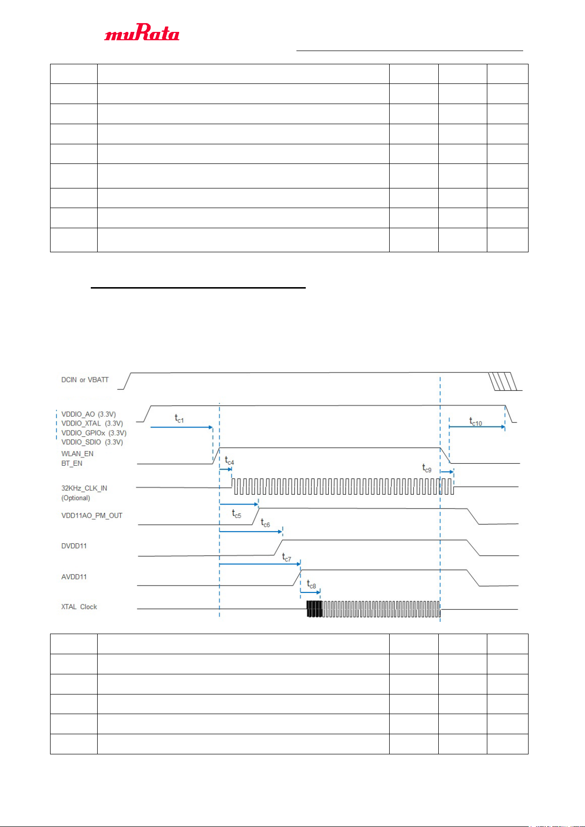
tc1
90% of 3.3 V to 0.7 V of both WLAN_EN and BT_EN
0 - μs
tc4
WLAN_EN valid to LF_CLK_IN input
0 - μs
tc5
WLAN_EN valid to VDD11AO_PM_OUT established
-
50
μs
tc6
WLAN_EN to DVDD11
-
3.5
ms
tc7
WLAN_EN to AVDD11
- 4 ms
VDD_3.3 (3.3V)
11.3. Case 3: All power rails supplied with 3.3 V
All power pins are connected to 3.3 V only include VDDIO_AO, VDDIO_XTAL, VDDIO_GPIOx.
Notes:
All host signals are either GND or floating before WLAN_EN/BT_EN =”high”, and after
WLAN_EN/BT_EN = Low.
11 / 38
Preliminary & Confidential
< Specification may be changed by Murata without notice >
Murata(China) Investment Co., Ltd.
Page 13

Preliminary Specification Number : SP-ZZ1PJ-F
tc8
AVDD11 to XTAL clock stable
1 - ms
tc9
WLAN_EN de-assert (“low”) to LF_CLK_IN de-assert (tristate
or low)
0 - μs
t
c10
Both WLAN_EN = low and BT_EN = low to 90% of 3.3 V
10 - μs
12. Digital I/O Requirements
TBD
13. INTERFACE TIMING AND AC CHARACTERISTICS
13.1. Bluetooth UART Timing
TBD
13.2. I2S Timing
TBD
13.3. SDIO Timing
TBD
12 / 38
Preliminary & Confidential
< Specification may be changed by Murata without notice >
Murata(China) Investment Co., Ltd.
Page 14
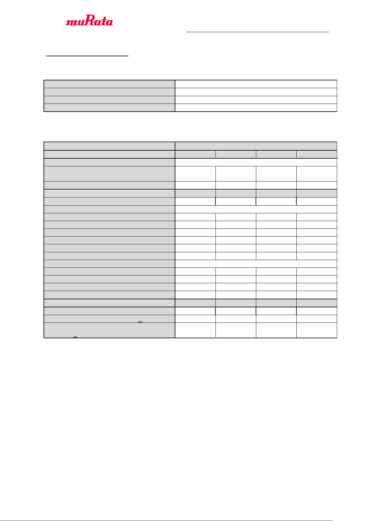
Preliminary Specification Number : SP-ZZ1PJ-F
Specification
IEEE802.11b
Mode
DSSS / CCK
Frequency
2412 to 2472 MHz
Data rate
1, 2, 5.5, 11Mbps
Items
Contents
- DC Characteristics -
min.
typ.
max.
unit
1. DC current
1) Tx mode (1024byte, 20usec interval)
*4) *5)
-
330 - mA
2) Rx mode
-
60 - mA
- Tx Characteristics -
min.
typ.
max.
unit
2. Output Power
-
19
-
dBm
3. Spectrum Mask margin
1) 1st side lobes(-30dBr)
0 - -
dB
2) 2nd side lobes(-50dBr)
0 - -
dB
4. Power-on and Power-down ramp
- 2.0
μsec
5. RF Carrier Suppression
15 - -
dB
6. Modulation Accuracy (EVM)
- - 35
%
7.Frequency tolerance
-20 - 20
ppm
8. Out band Spurious Emissions
1) 30-1000MHz
- - -36
dBm
2) 1000-12750MHz
- - -30
dBm
3) 1800-1900MHz
-47
dBm
4) 5150-5300MHz
- - -47
dBm
- Rx Characteristics -
min.
typ.
max.
unit
9. Minimum Input Level Sensitivity
-
-89
-76
dBm
10. Maximum Input Level (PER < 8%)
-10 - -
dBm
11. Adjacent Channel Rejection
(FER < 8%)
35 - -
dB
14. DC / RF Characteristics
14.1. DC/RF Characteristics for IEEE802.11b - 2.4GHz
Conditions : 25deg.C,
VDD_3P3,VDDIO_SDIO,VDDIO_GPIO1,VDDIO_GPIO2,VDDIO_XTAL,VDDIO_AO=3.3V
Output power setting=19 dBm, 11Mbps mode unless otherwise specified.
13 / 38
*4): Defined when output power setting is 19 dBm at Murata module antenna pad
*5): Data rate is 1Mbps
< Specification may be changed by Murata without notice >
Preliminary & Confidential
Murata(China) Investment Co., Ltd.
Page 15
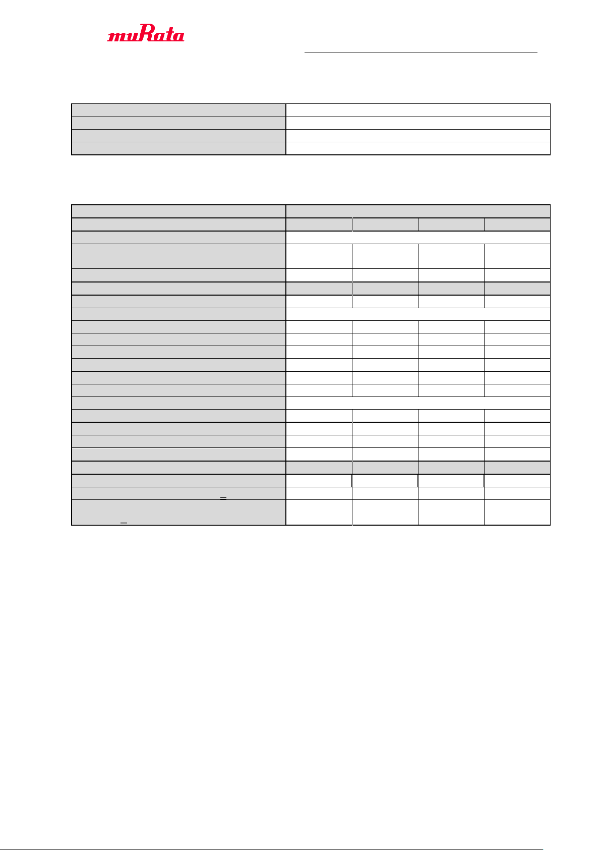
Preliminary Specification Number : SP-ZZ1PJ-F
Specification
IEEE802.11g
Mode
OFDM
Frequency
2412 to 2472 MHz
Data rate
6, 9, 12, 18, 24, 36, 48, 54Mbps
Items
Contents
- DC Characteristics -
min.
typ.
max.
unit
1. DC current
1) Tx mode (1024byte, 20usec interval)
*6) *7)
-
310 - mA
2) Rx mode
-
60 - mA
- Tx Characteristics -
min.
typ.
max.
unit
2. Output Power
-
17 - dBm
3. Spectrum Mask margin
1) 9MHz to 11MHz (0~ -20dBr)
0 - -
dB
2) 11MHz to 20MHz (-20~ -28dBr)
0 - -
dB
3) 20MHz to 30MHz (-28~ -40dBr)
0 - -
dB
4) 30MHz to 33MHz (-40dBr)
0 - -
dB
4. Constellation Error (EVM)
- - -25
dB
5.Frequency tolerance
-20 - 20
ppm
6. Out band Spurious Emissions
1) 30-1000MHz
- - -36
dBm
2) 1000-12750MHz
- - -30
dBm
3) 1800-1900MHz
-47
dBm
4) 5150-5300MHz
- - -47
dBm
- Rx Characteristics -
min.
typ.
max.
unit
7. Minimum Input Level Sensitivity
-
-74
-65
dBm
8. Maximum Input Level (PER < 10%)
-20 - -
dBm
9. Adjacent Channel Rejection
(PER < 10%)
-1 - -
dB
14.2. DC/RF Characteristics for IEEE802.11g - 2.4GHz
Conditions : 25deg.C,
VDD_3P3,VDDIO_SDIO,VDDIO_GPIO1,VDDIO_GPIO2,VDDIO_XTAL,VDDIO_AO=3.3V
Output power setting=17 dBm, 54Mbps mode unless otherwise specified.
14 / 38
*6): Defined when output power setting is 18dBm at Murata module antenna pad
*7): Data rate is 6Mbps
< Specification may be changed by Murata without notice >
Preliminary & Confidential
Murata(China) Investment Co., Ltd.
Page 16
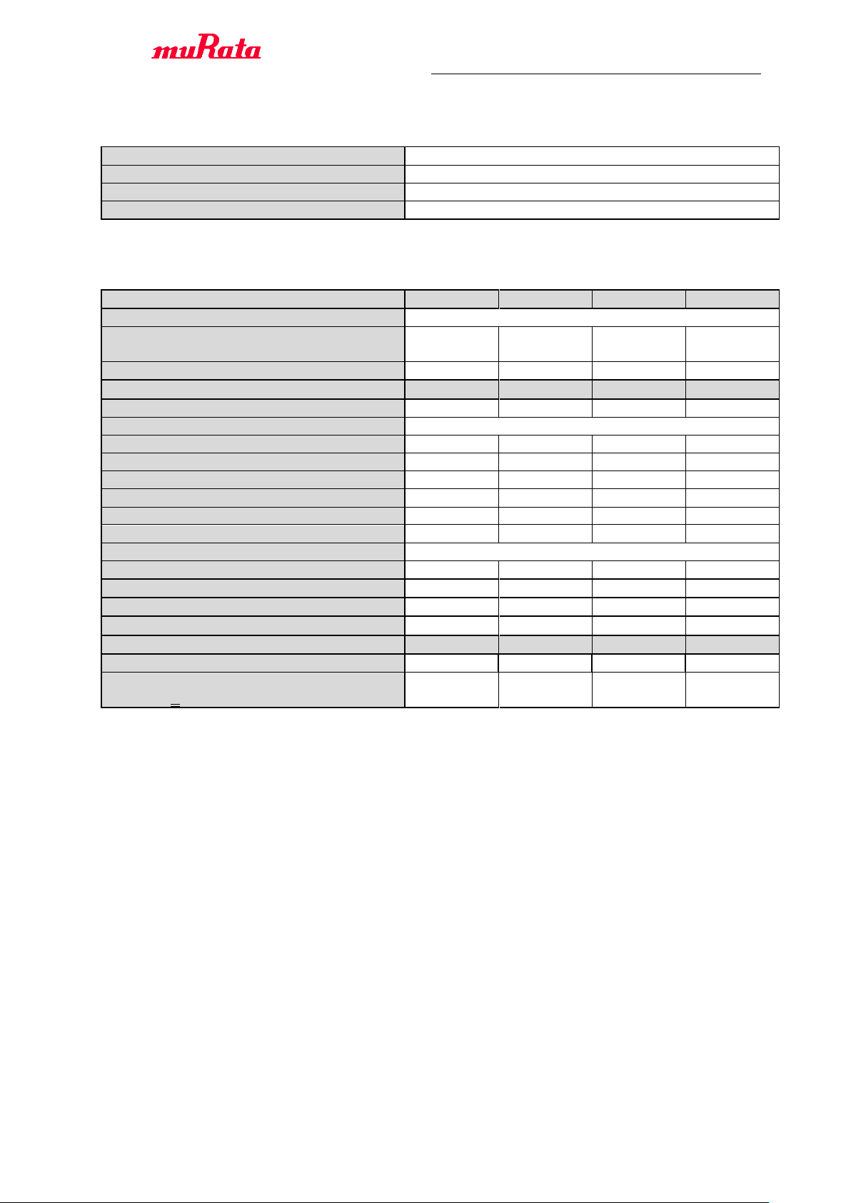
Preliminary Specification Number : SP-ZZ1PJ-F
Specification
IEEE802.11n
Mode
OFDM
Frequency
2412 to 2472 MHz
Data rate
MCS0-MCS7
- DC Characteristics -
min.
typ.
max.
unit
1. DC current
1) Tx mode (1024byte, 20usec interval)
*8)*9)
-
310 - mA
2) Rx mode
-
60 - mA
- Tx Characteristics -
min.
typ.
max.
unit
2. Output Power
-
16 - dBm
3. Spectrum Mask
1) 9MHz to 11MHz (0 ~ -20dBr)
0 - -
dB
2) 11MHz to 20MHz (-20 ~ -28dBr)
0 - -
dB
3) 20MHz to 30MHz (-28 ~ -45dBr)
0 - -
dB
4) 30MHz to 33MHz (-45dBr)
0 - -
dB
4. Constellation Error (EVM)
- - -27
dB
5.Frequency tolerance
-20 - 20
ppm
6. Out band Spurious Emissions
1) 30-1000MHz
- - -36
dBm
2) 1000-12750MHz
- - -30
dBm
3) 1800-1900MHz
-47
dBm
4) 5150-5300MHz
- - -47
dBm
- Rx Characteristics -
min.
typ.
max.
unit
6. Minimum Input Level Sensitivity
-
-71
-64
dBm
7. Adjacent Channel Rejection
(PER < 10%)
-2 - -
dB
14.3. DC/RF Characteristics for IEEE802.11n – 2.4GHz
Conditions : 25deg.C,
VDD_3P3,VDDIO_SDIO,VDDIO_GPIO1,VDDIO_GPIO2,VDDIO_XTAL,VDDIO_AO=3.3V
Output power setting=16 dBm, BW=20MHz, MCS7 unless otherwise specified.
15 / 38
*8): Defined when output power setting is 18 dBm at Murata module antenna pad
*9): Data rate is MCS0
< Specification may be changed by Murata without notice >
Preliminary & Confidential
Murata(China) Investment Co., Ltd.
Page 17
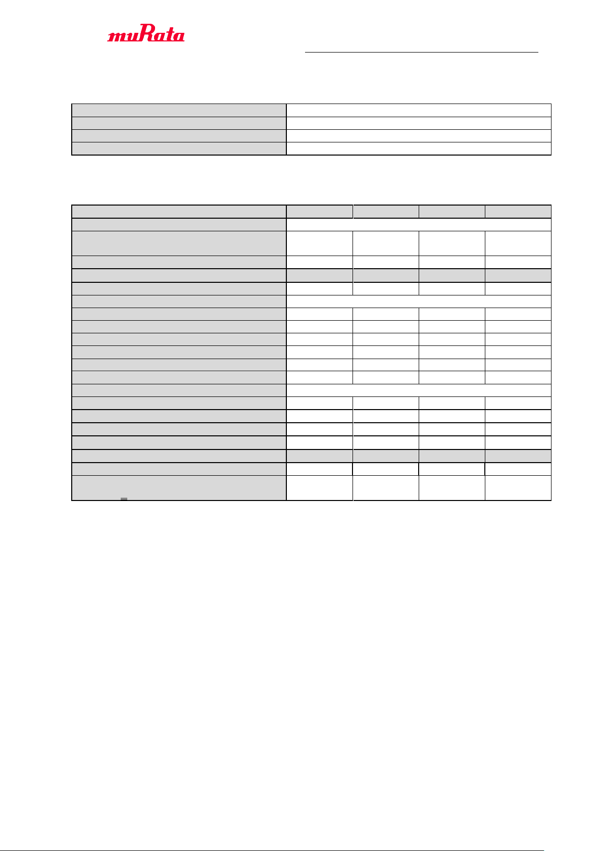
Preliminary Specification Number : SP-ZZ1PJ-F
Specification
IEEE802.11ac
Mode
OFDM
Frequency
2412 to 2472 MHz
Data rate
MCS0-MCS9
- DC Characteristics -
min.
typ.
max.
unit
1. DC current
1) Tx mode (1024byte, 20usec interval)
*8)*9)
-
290 - mA
2) Rx mode
-
62 - mA
- Tx Characteristics -
min.
typ.
max.
unit
2. Output Power
-
14 - dBm
3. Spectrum Mask
1) 9MHz to 11MHz (0 ~ -20dBr)
0 - -
dB
2) 11MHz to 20MHz (-20 ~ -28dBr)
0 - -
dB
3) 20MHz to 30MHz (-28 ~ -45dBr)
0 - -
dB
4) 30MHz to 33MHz (-45dBr)
0 - -
dB
4. Constellation Error (EVM)
- - -32
dB
5.Frequency tolerance
-20 - 20
ppm
6. Out band Spurious Emissions
1) 30-1000MHz
- - -36
dBm
2) 1000-12750MHz
- - -30
dBm
3) 1800-1900MHz
-47
dBm
4) 5150-5300MHz
- - -47
dBm
- Rx Characteristics -
min.
typ.
max.
unit
6. Minimum Input Level Sensitivity
-
-63
-54
dBm
7. Adjacent Channel Rejection
(PER < 10%)
-2 - -
dB
14.4. DC/RF Characteristics for IEEE802.11ac – 2.4GHz
Conditions : 25deg.C,
VDD_3P3,VDDIO_SDIO,VDDIO_GPIO1,VDDIO_GPIO2,VDDIO_XTAL,VDDIO_AO=3.3V
Output power setting=14 dBm, MCS9,BW=40MHz unless otherwise specified.
16 / 38
*8): Defined when output power setting is 16 dBm at Murata module antenna pad
*9): Data rate is MCS0
< Specification may be changed by Murata without notice >
Preliminary & Confidential
Murata(China) Investment Co., Ltd.
Page 18
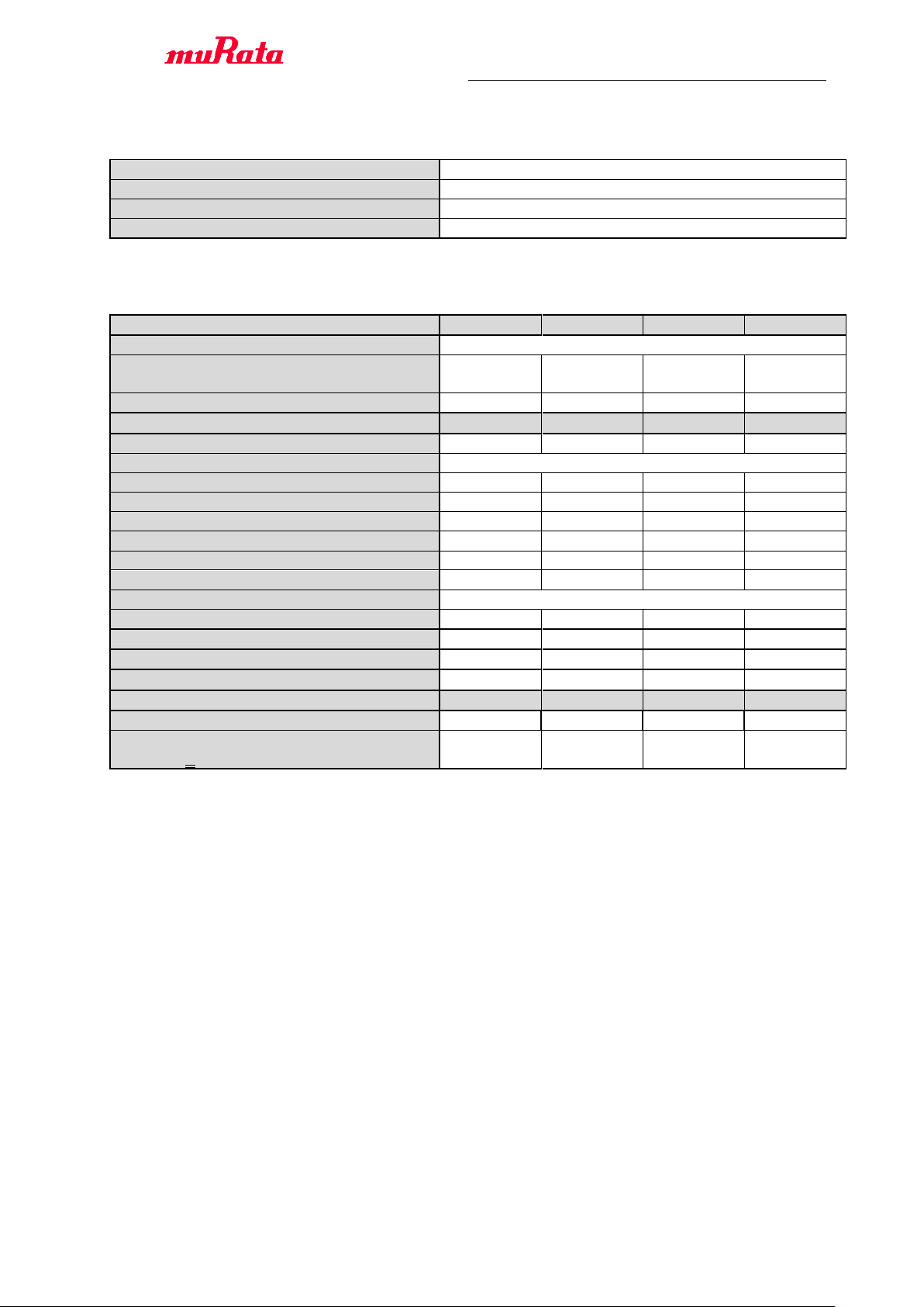
Preliminary Specification Number : SP-ZZ1PJ-F
Specification
IEEE802.11a
Mode
OFDM
Frequency
5180 to 5825MHz
Data rate
6, 9, 12, 18, 24, 36, 48, 54Mbps
- DC Characteristics -
min.
typ.
max.
unit
1. DC current
1) Tx mode (1024byte, 20usec interval)
*8)*9)
-
420 - mA
2) Rx mode
-
80 - mA
- Tx Characteristics -
min.
typ.
max.
unit
2. Output Power
-
11 - dBm
3. Spectrum Mask
1) 9MHz to 11MHz (0 ~ -20dBr)
0 - -
dB
2) 11MHz to 20MHz (-20 ~ -28dBr)
0 - -
dB
3) 20MHz to 30MHz (-28 ~ -45dBr)
0 - -
dB
4) 30MHz to 33MHz (-45dBr)
0 - -
dB
4. Constellation Error (EVM)
- - -25
dB
5.Frequency tolerance
-20 - 20
ppm
6. Out band Spurious Emissions
1) 30-1000MHz
- - -36
dBm
2) 1000-12750MHz
- - -30
dBm
3) 1800-1900MHz
-47
dBm
4) 5150-5300MHz
- - -47
dBm
- Rx Characteristics -
min.
typ.
max.
unit
6. Minimum Input Level Sensitivity
-
-71
-65
dBm
7. Adjacent Channel Rejection
(PER < 10%)
-1 - -
dB
14.5. DC/RF Characteristics for IEEE802.11a - 5GHz
Conditions : 25deg.C,
VDD_3P3,VDDIO_SDIO,VDDIO_GPIO1,VDDIO_GPIO2,VDDIO_XTAL,VDDIO_AO=3.3V
Output power setting= 11 dBm, 54Mbps unless otherwise specified.
17 / 38
*8): Defined when output power setting is 14 dBm at Murata module antenna pad
*9): Data rate is 6Mbps
< Specification may be changed by Murata without notice >
Preliminary & Confidential
Murata(China) Investment Co., Ltd.
Page 19
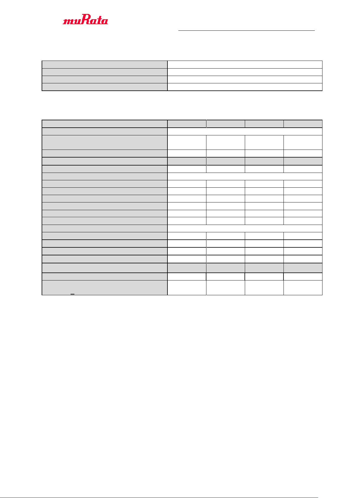
Preliminary Specification Number : SP-ZZ1PJ-F
Specification
IEEE802.11n
Mode
OFDM
Frequency
5180 to 5825MHz
Data rate
MCS0-MCS7
- DC Characteristics -
min.
typ.
max.
unit
1. DC current
1) Tx mode (1024byte, 20usec interval)
*8)*9)
-
420 - mA
2) Rx mode
-
80 - mA
- Tx Characteristics -
min.
typ.
max.
unit
2. Output Power
-
10 - dBm
3. Spectrum Mask
1) 9MHz to 11MHz (0 ~ -20dBr)
0 - -
dB
2) 11MHz to 20MHz (-20 ~ -28dBr)
0 - -
dB
3) 20MHz to 30MHz (-28 ~ -45dBr)
0 - -
dB
4) 30MHz to 33MHz (-45dBr)
0 - -
dB
4. Constellation Error (EVM)
- - -32
dB
5.Frequency tolerance
-20 - 20
ppm
6. Out band Spurious Emissions
1) 30-1000MHz
- - -36
dBm
2) 1000-12750MHz
- - -30
dBm
3) 1800-1900MHz
-47
dBm
4) 5150-5300MHz
- - -47
dBm
- Rx Characteristics -
min.
typ.
max.
unit
6. Minimum Input Level Sensitivity
-
-69
-64
dBm
7. Adjacent Channel Rejection
(PER < 10%)
-2 - -
dB
14.6. DC/RF Characteristics for IEEE802.11n - 5GHz
Conditions : 25deg.C,
VDD_3P3,VDDIO_SDIO,VDDIO_GPIO1,VDDIO_GPIO2,VDDIO_XTAL,VDDIO_AO=3.3V
Output power setting= 10 dBm, BW=20MHz ,MCS7 unless otherwise specified.
18 / 38
*8): Defined when output power setting is 14 dBm at Murata module antenna pad
*9): Data rate is MCS0
< Specification may be changed by Murata without notice >
Preliminary & Confidential
Murata(China) Investment Co., Ltd.
Page 20
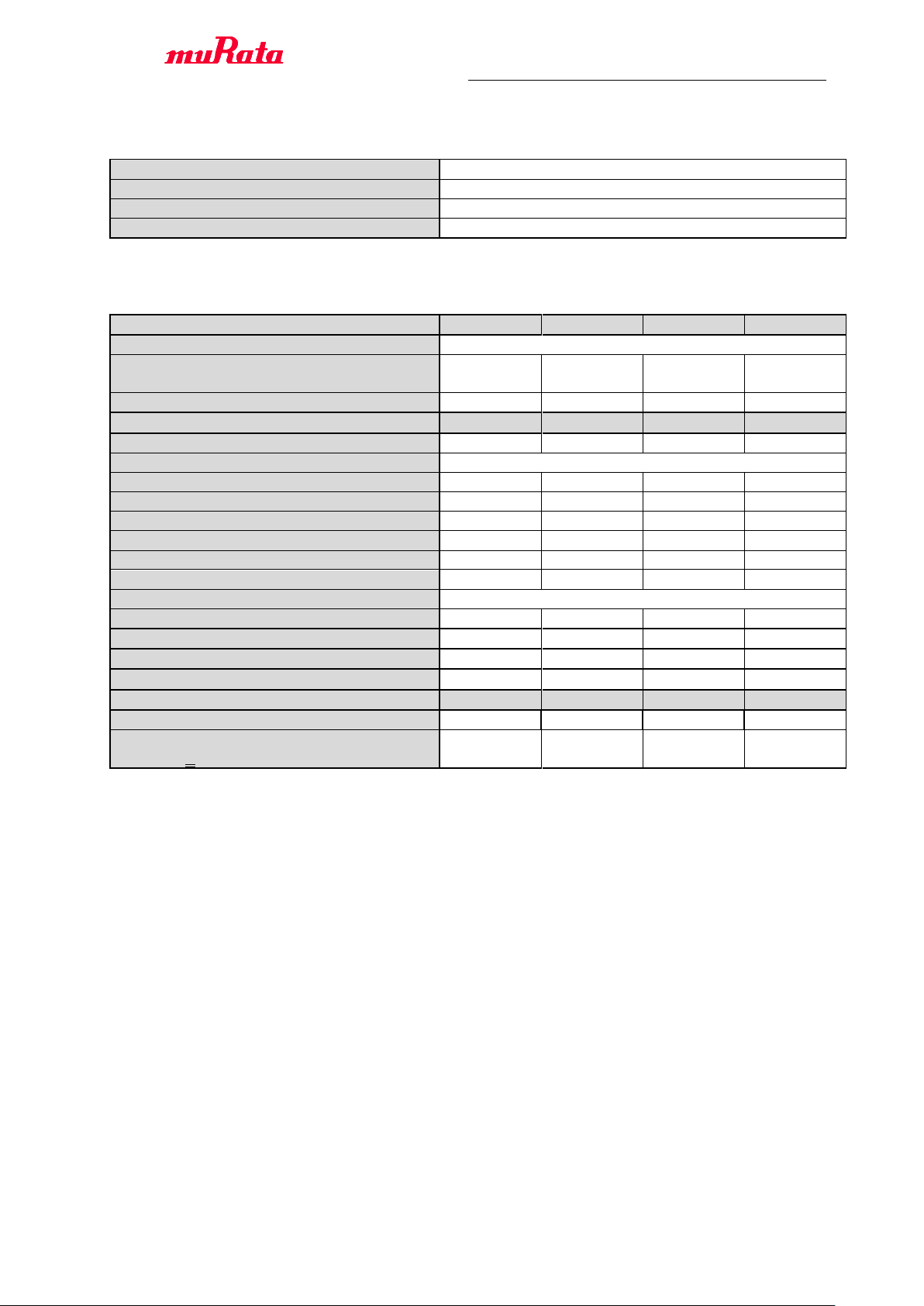
Preliminary Specification Number : SP-ZZ1PJ-F
Specification
IEEE802.11ac
Mode
OFDM
Frequency
5210 to 5775MHz
Data rate
MCS0-MCS9
- DC Characteristics -
min.
typ.
max.
unit
1. DC current
1) Tx mode (1024byte, 20usec interval)
*8)*9)
-
370 - mA
2) Rx mode
-
90 - mA
- Tx Characteristics -
min.
typ.
max.
unit
2. Output Power
- 8 -
dBm
3. Spectrum Mask
1) 9MHz to 11MHz (0 ~ -20dBr)
0 - -
dB
2) 11MHz to 20MHz (-20 ~ -28dBr)
0 - -
dB
3) 20MHz to 30MHz (-28 ~ -45dBr)
0 - -
dB
4) 30MHz to 33MHz (-45dBr)
0 - -
dB
4. Constellation Error (EVM)
- - -32
dB
5.Frequency tolerance
-20 - 20
ppm
6. Out band Spurious Emissions
1) 30-1000MHz
- - -36
dBm
2) 1000-12750MHz
- - -30
dBm
3) 1800-1900MHz
-47
dBm
4) 5150-5300MHz
- - -47
dBm
- Rx Characteristics -
min.
typ.
max.
unit
6. Minimum Input Level Sensitivity
-
-59
-51
dBm
7. Adjacent Channel Rejection
(PER < 10%)
-2 - -
dB
14.7. DC/RF Characteristics for IEEE802.11ac - 5GHz
Conditions : 25deg.C,
VDD_3P3,VDDIO_SDIO,VDDIO_GPIO1,VDDIO_GPIO2,VDDIO_XTAL,VDDIO_AO=3.3V
Output power setting= 8 dBm, BW=80MHz ,MCS9 unless otherwise specified.
19 / 38
*8): Defined when output power setting is 12dBm at Murata module antenna pad
*9): Data rate is MCS0
< Specification may be changed by Murata without notice >
Preliminary & Confidential
Murata(China) Investment Co., Ltd.
Page 21
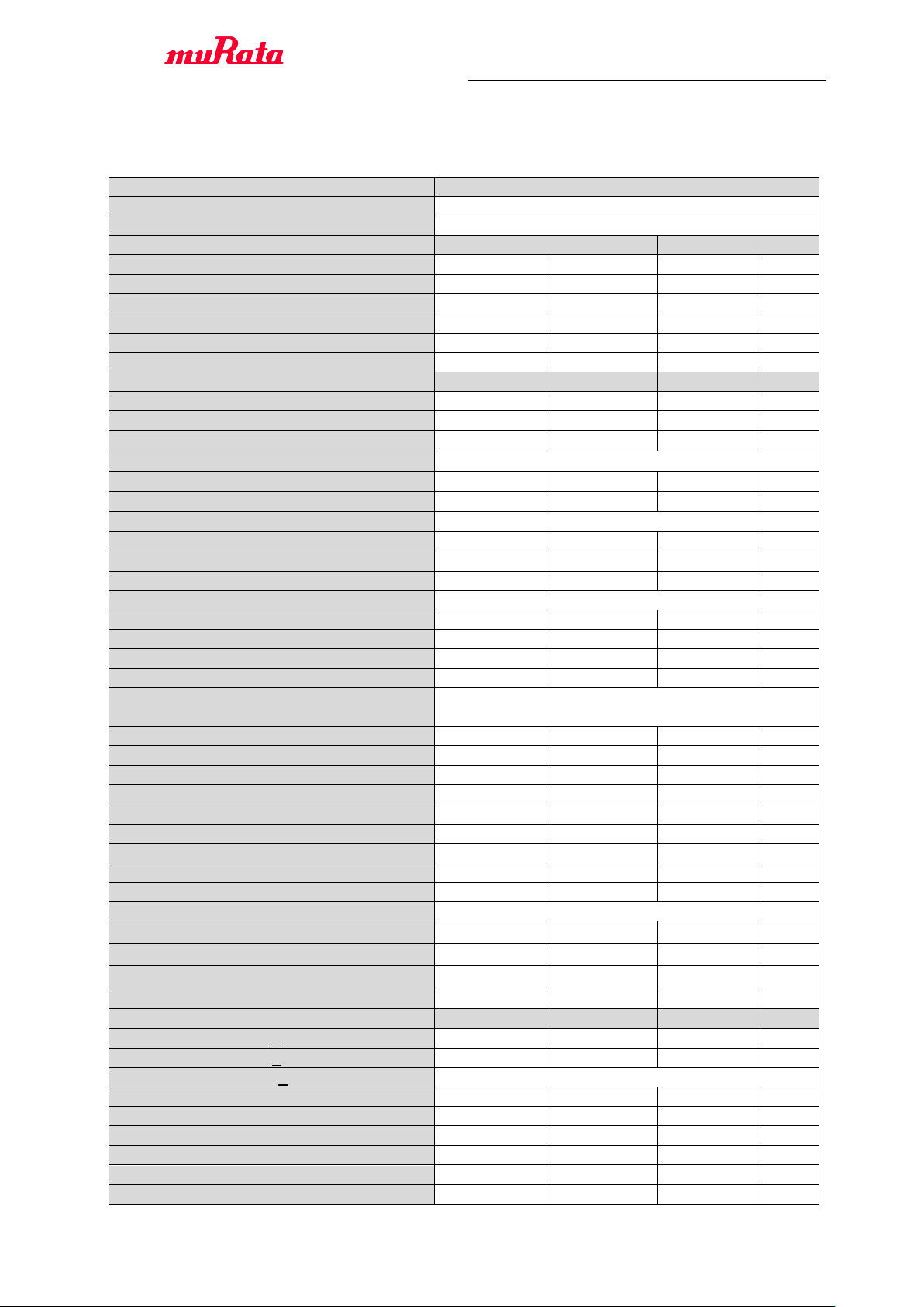
Preliminary Specification Number : SP-ZZ1PJ-F
Items
Contents
Bluetooth specification (power class)
Version 2.1 + EDR (Class1)
Channel frequency (spacing)
2402 to 2480 MHz (1MHz)
Current Consumption
Min.
Typ.
Max.
unit
(a) Tx=DH5
-
55
-
mA
(b) Tx=2DH5
-
50
-
mA
(c) Tx=3DH5
-
50
-
mA
(d) Rx=DH5
-
22
-
mA
(e) Rx=2DH5
-
22
-
mA
(f) Rx=3DH5
-
22
-
mA
Transmitter
Min.
Typ.
Max.
Unit
Output Power@DH5
- 9 -
dBm
Frequency range
2402
-
2480
MHz
20dB bandwidth
-
950
1000
MHz
Adjacent Channel Power *1
(a) [M-N] =2
- - -20
dBm
(b) [M-N] ≥3
- - -40
dBm
Modulation characteristics
(a) Modulation Δf1avg
140
-
175
kHz
(b) Modulation Δf2max
115 -
kHz
(c) Modulation Δf2avg / Δf1avg
0.8 - -
Carrier Frequency Drift
(a) 1slot
-25
-
+25
kHz
(b) 3slot / 5slot
-40
-
+40
kHz
(c) Maximum drift rate
- 20
kHz/50us
EDR Relative Power
-4 - +1
dB
EDR Carrier Frequency Stability and
Modulation Accuracy
(a) ωi
-75
-
+75
kHz
(b) ωi+ωo
-75
-
+75
kHz
(c) ωo
-10
-
+10
kHz
(d) RMS DEVM (DQPSK)
- - 20
%
(e) Peak DEVM (DQPSK)
- - 35
%
(f) 99% DEVM (DQPSK)
- - 30
%
(g) RMS DEVM (8DPSK)
- - 13
%
(h) Peak DEVM (8DPSK)
- - 25
%
(i) 99% DEVM (8DPSK)
-
-
20
%
Spurious Emissions
(a) 10MHz≦f<2387MHz
- - -36
dBm
(b) 2387MHz≦f<2400MHz
- - -30
dBm
(c) 2483.5MHz<f≦2496.5MHz
-47
dBm
(d) 2496.5MHz<f≦8GHz
- - -47
dBm
Receiver
Min.
Typ.
Max.
unit
BDR Sensitivity (BER<0.1%)
-
-92
-80
dBm
EDR Sensitivity (BER<0.007%)@8DPSK
-
-87
-77
dBm
C/I Performance (BER<0.1%) *2
(a) co-channel
- - 11
dB
(b) 1MHz
- - 0
dB
(c) 2MHz
- - -30
dB
(d) 3MHz
- - -40
dB
(e) image (+4MHz)
- - -9
dB
(f) image +/- 1MHz
- - -20
dB
14.8. DC/RF Characteristics for Bluetooth
Conditions : 25deg.C,
VDD_3P3,VDDIO_SDIO,VDDIO_GPIO1,VDDIO_GPIO2,VDDIO_XTAL,VDDIO_AO=3.3V
20 / 38
< Specification may be changed by Murata without notice >
Preliminary & Confidential
Murata(China) Investment Co., Ltd.
Page 22
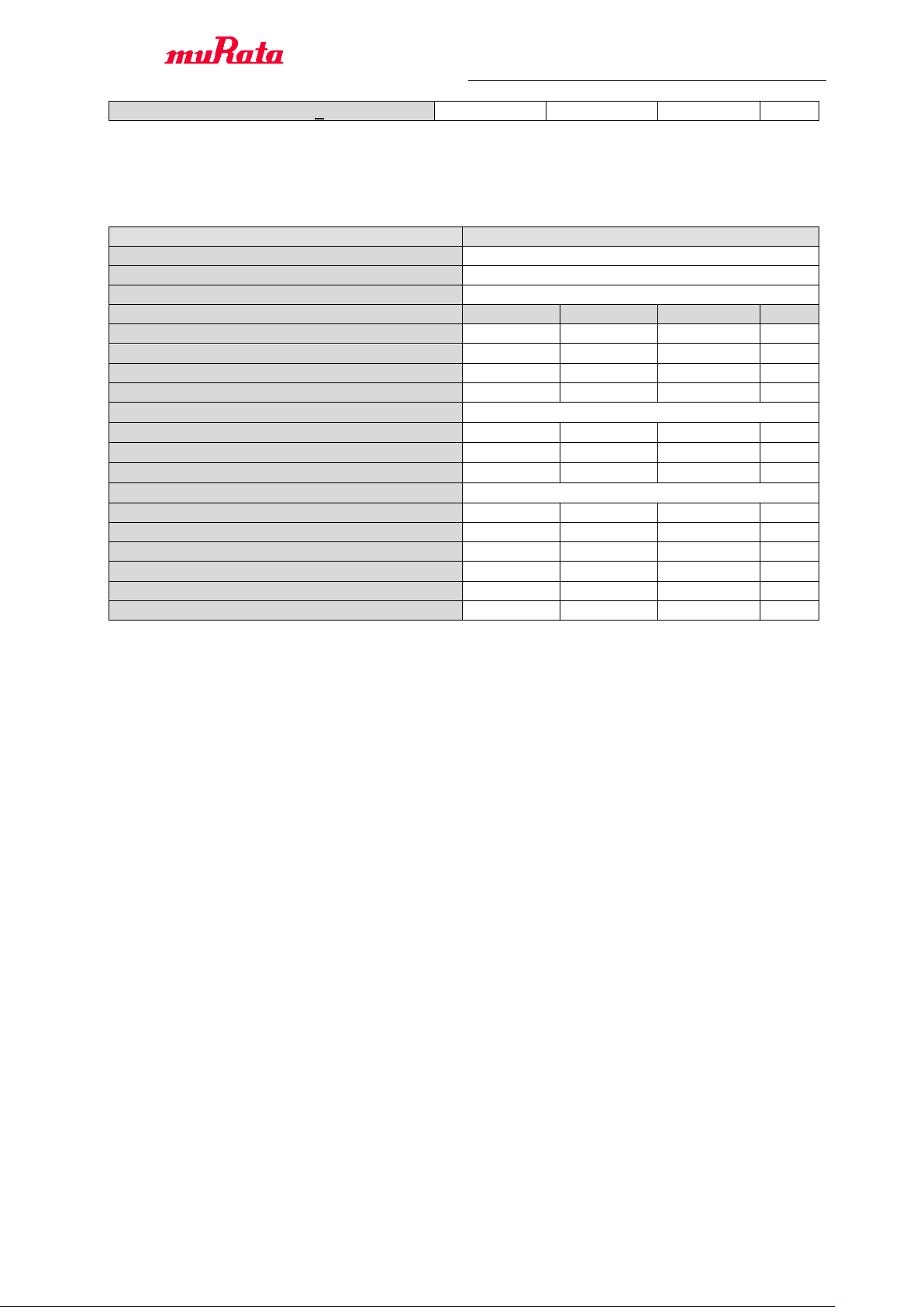
Preliminary Specification Number : SP-ZZ1PJ-F
Maximum Input Level (BER<0.1%)
-20 - -
dBm
Items
Contents
Bluetooth specification (power class)
Version 4.1(LE)
Channel frequency (spacing)
2402 to 2480 MHz (2MHz)
Number of RF Channel
40
Item / Condition
Min.
Typ.
Max.
Unit
Center Frequency
2402
-
2480
MHz
Channel Spacing
- 2 -
MHz
Number of RF channel
-
40
-
-
Output power
- 4 10
dBm
Modulation Characteristics
1) Δf1
avg
225 - 275
kHz
2) Δf2
max
(at 99.9%)
185 - -
kHz
3) Δf2
avg
/ Δf1
avg
0.8 - -
-
Carrier frequency offset and drift
1) Frequency offset
- - 150
kHz
2) Frequency drift
- - 50
kHz
3) Drift rate
- - 20
kHz
Receiver sensitivity (PER < 30.8%)
-
-96
-70
dBm
Maximum input signal level (PER < 30.8%)
-10 - -
dBm
PER Report Integrity (-30dBm input)
50 - 65.4
%
*1: Up to three spurious responses within Bluetooth limits are allowed.
*2: Up to five spurious responses within Bluetooth limits are allowed.
14.9. DC/RF Characteristics for Bluetooth (LE)
Conditions : 25deg.C,
VDD_3P3,VDDIO_SDIO,VDDIO_GPIO1,VDDIO_GPIO2,VDDIO_XTAL,VDDIO_AO=3.3V
21 / 38
< Specification may be changed by Murata without notice >
Preliminary & Confidential
Murata(China) Investment Co., Ltd.
Page 23
Preliminary Specification Number : SP-ZZ1PJ-F
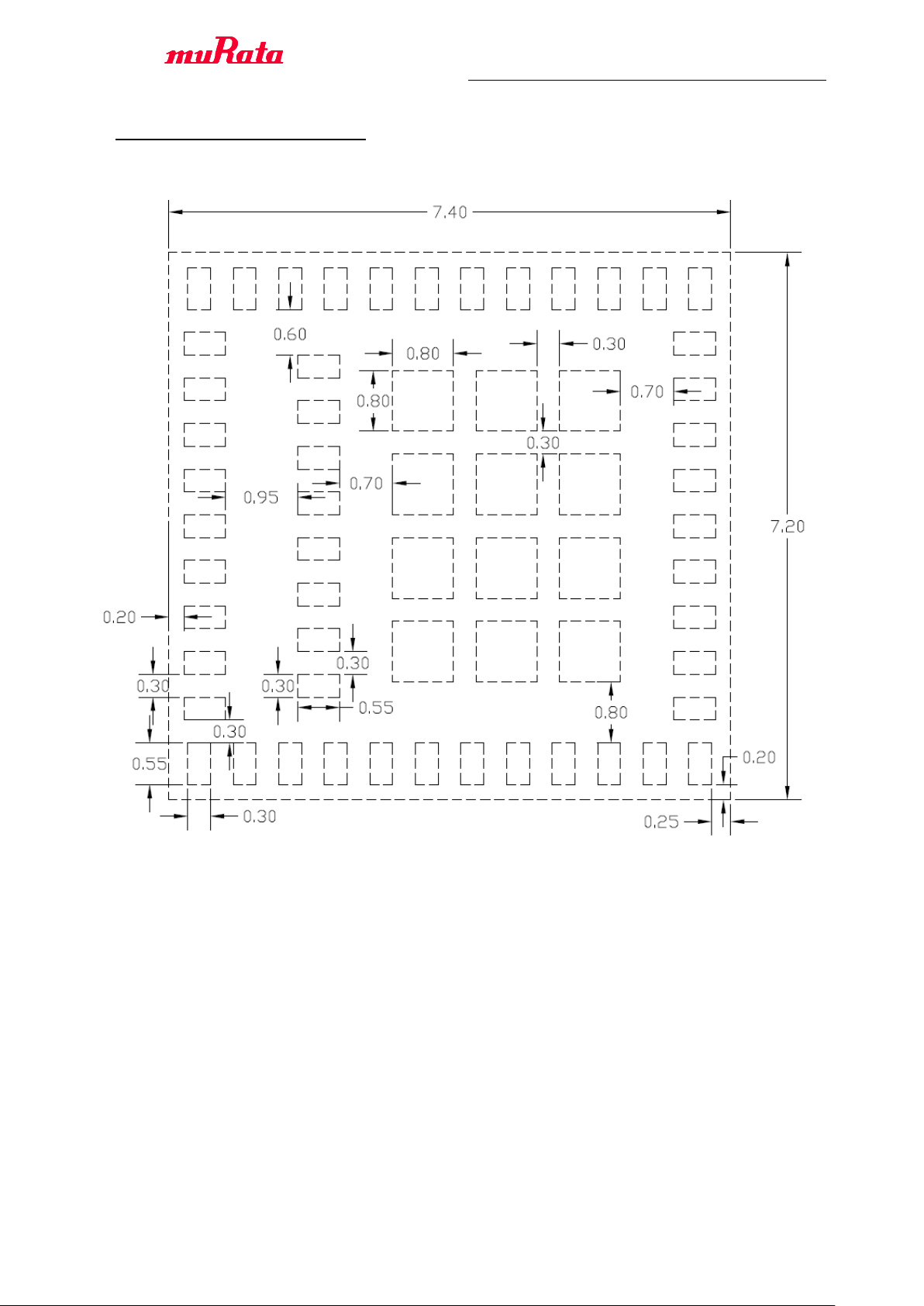
15. LAND PATTERN (TOP VIEW)
22 / 38
<Top View>
***Stencil design:
For 0.3×0.55mm electrodes, stencil pad is 0.24mm*0.44mm and should put in the center of the each
conductor.
For 0.8×0.8mm electrodes, stencil pad is 0.66mm*0.66mm and should put in the center of the each
conductor.
***This is based on Murata’s condition using the thickness of the stencil 100 um.
So this is just the recommendation and needs to modify based on your condition.
Preliminary & Confidential
< Specification may be changed by Murata without notice >
Murata(China) Investment Co., Ltd.
Page 24
Preliminary Specification Number : SP-ZZ1PJ-F
SDIO_C MD
LBEE5ZZ1PJ -164
GND1VBUCK_GN D_PM2PWM_PM3VDD11_PM
4
GND
5
SDIO_D ATA36SDIO_D ATA27SDIO_D ATA18SDIO_D ATA0
9
GND
43
LTE_UAR T_RXD
44
LTE_UAR T_TXD
45
CLK_REQ
46
DBG_UAR T_TXD
47
DBG_UAR T_RXD
48
QOW
49
GND
50
2G_WIF I/BT_RF_IN
22
GND
23
ANT
24
GND
25
3D_FR AME_SYNC
26
HCI _UART_RXD
27
HCI _UART_TXD
28
HCI _UART_RTS29HCI _UART_CTS
30
GND
51
GND
52
GND
53
GND
54
GND
55
GND
56
GND
57
GND
58
GND
59
GND
60
GND
61
GND
62
PCM_CLK
31
PCM_SYN C
32
PCM_IN
33
PCM_OUT
34
GND
35
VDDI O_XTAL36VDDI O_GPIO1
37
GND
38
WLAN_EN
39
BT_EN
40
VDD_3P3
41
VDDI O_AO
42
SDIO_C MD10SDIO_C LK
11
VDDI O_SDIO
12
SDIO_I NTERRUPT_L
13
GND
14
32KHZ_C LK_IN
15
VDDI O_GPIO2
16
HCI _UART_WAKEH OST
17
WLAN_R F_KILL_L
18
GND
19
2G_WIF I/BT_RF_OUT
20
GND
21
BT_UART_CTS
BT_UART_RTS
BT_UART_RXD
BT_UART_TXD
LTE_UAR T_TXD
LTE_UAR T_RXD
WL_DEV_W AKEUP_HOST
32KHz Cloc k in
C7
47uF
DBG_UAR T_TXD
DBG_UAR T_RXD
BT_PCM_OUT
J3
RF-SOC KET_0
2
3
4
1
5
SMA connector
BT_DEV_WAKEUP_H OST
R10
10K
BT_PCM_SYNC
BT_EN
BT_PCM_CLK
SDIO_C LK
BT_PCM_IN
WLAN_EN
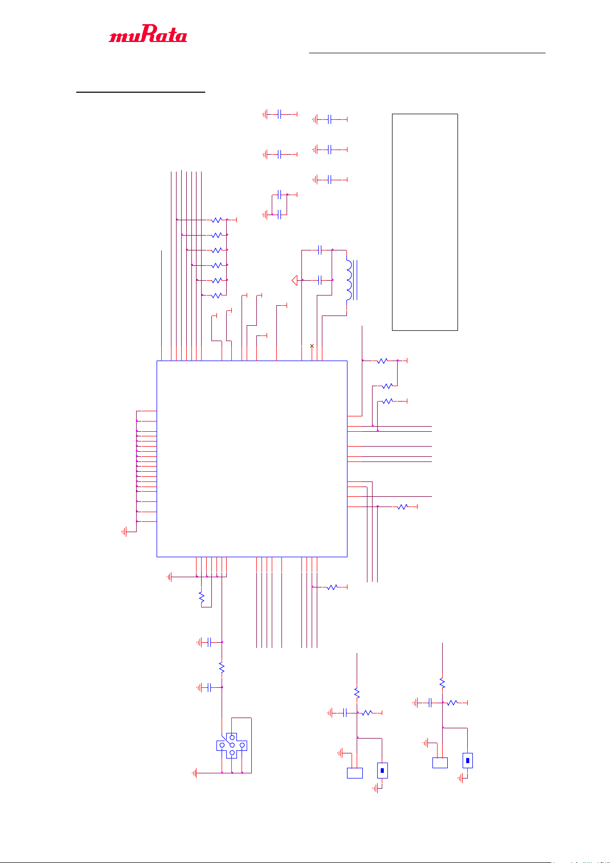
1. VDD_3V3 is powered by 3.3V typically.
2. VDDIO_AO, VDDIO_GPIO1, VDDIO_GPIO2, VDDIO_XTAL,
VDDIO_SDIO can be powered by 1.8V or 3.3V.
It should match the VIO voltage from host.
For the each I/O voltage group of 1PJ module, please
refer to 1PJ module datasheet.
Notes for the power supply voltage:
WLAN_EN
OQW
R5
10K
R17 0R
R13
NU
VDDI O_AO
R12
NU
R11
NU
R3
10K
R8 27
C2
0.1uF
R7
10K
VDDI O_GPIO2
BT_HOST_WAKEUP_DEV/ 3D_FRAME_SYN C
TOLERANCE = 20%
L1 1.5uH
VDDI O_AO
C3
1uF
VDD_3V3
VDDI O_GPIO1
VDDI O_GPIO2
WLAN Reset
VDDI O_XTAL
J2
CON2
1
2
R9
10K
VDDI O_GPIO1
WLAN_R F_KILL_L
VDDI O_SDIO
CLK_REQ
R6
10K
VDDI O_AO
R4
10K
VDDI O_GPIO2
R15
NU
R14
10K
SDIO_D ATA3
SW2 SKQY A
1 2
SDIO_D ATA2
VDDI O_SDIO
SDIO_D ATA1
R2 27
BT_EN
R1
10K
C1
0.1uF
BT Reset
VDDI O_AO
SW1 SKQY A
1 2
J1
CON2
1
2
R16 0R
SDIO_D ATA0
VDDI O_GPIO1
VDDI O_SDIOVDDI O_XTALVDDI O_GPIO2
VDDI O_AO
C11
0.1uF
C10
10uF
C6
1uF
C5
2.2uF
C4
10uF
C8
1uF
C9
1uF
C13
NU
VDD_3V3
C12
NU
16. REFERENCE CIRCUIT
23 / 38
< Specification may be changed by Murata without notice >
Preliminary & Confidential
Murata(China) Investment Co., Ltd.
Page 25
Preliminary Specification Number : SP-ZZ1PJ-F
W
16+/-0.2
P2
2+/-0.1
F
7.5+/-0.1
A0
7.8+/-0.1
T
0.3+/-0.05
B0
7.6+/-0.1
E
1.75+/-0.1
K0
1.25+/-0.1
P
12+/-0.1
D0
1.5+0.1/-0
P0
4+/-0.1
D1
1.5+/-0.1
W1
25.5 +/-1.0
W2
29.5 +/-1.0
Feeding direction
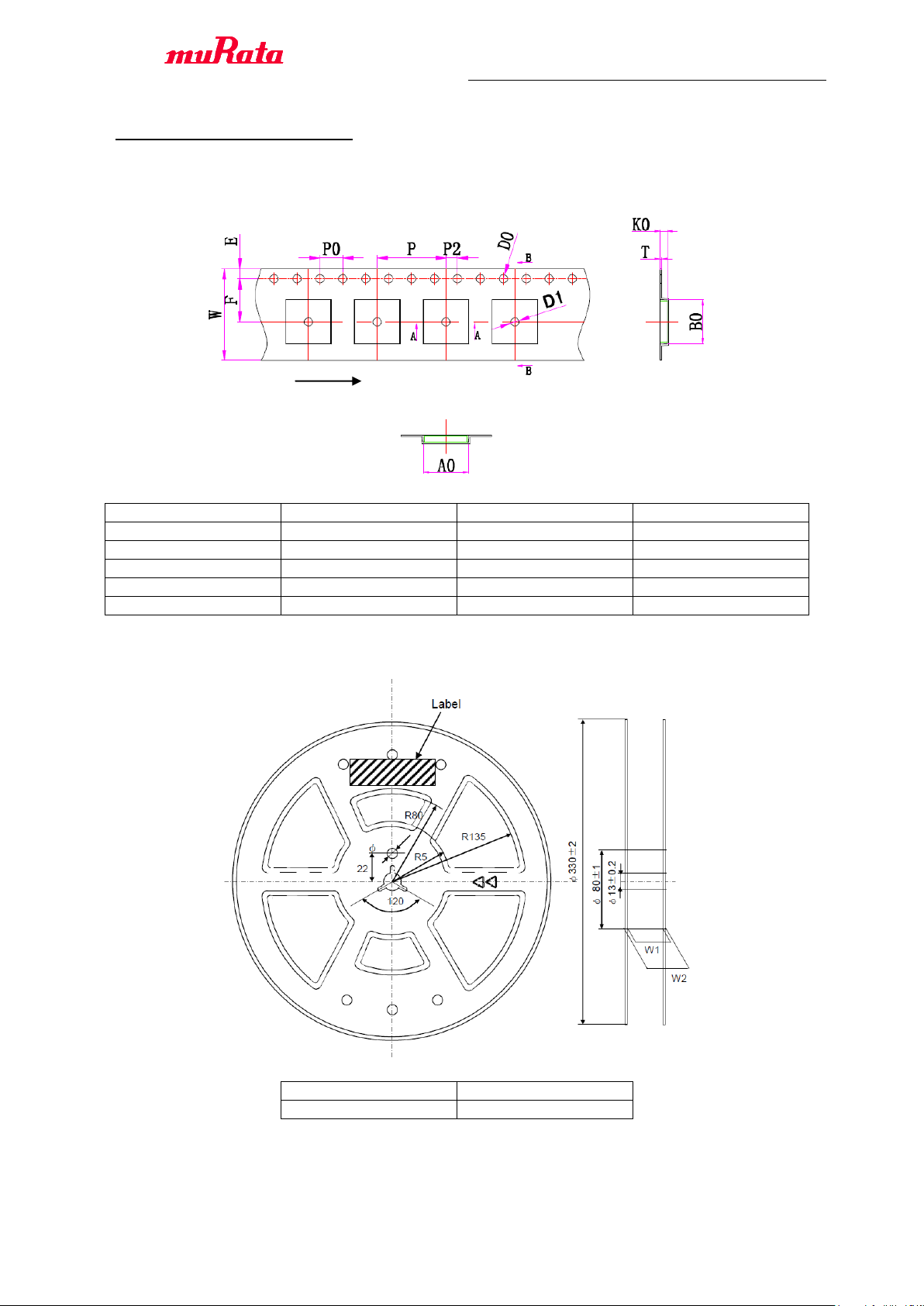
17. TAPE AND REEL PACKING
(1) Dimensions of Tape (Plastic tape)
24 / 38
(2) Dimensions of Reel
Unit: mm
Unit: mm
Preliminary & Confidential
< Specification may be changed by Murata without notice >
Murata(China) Investment Co., Ltd.
Page 26
Preliminary Specification Number : SP-ZZ1PJ-F
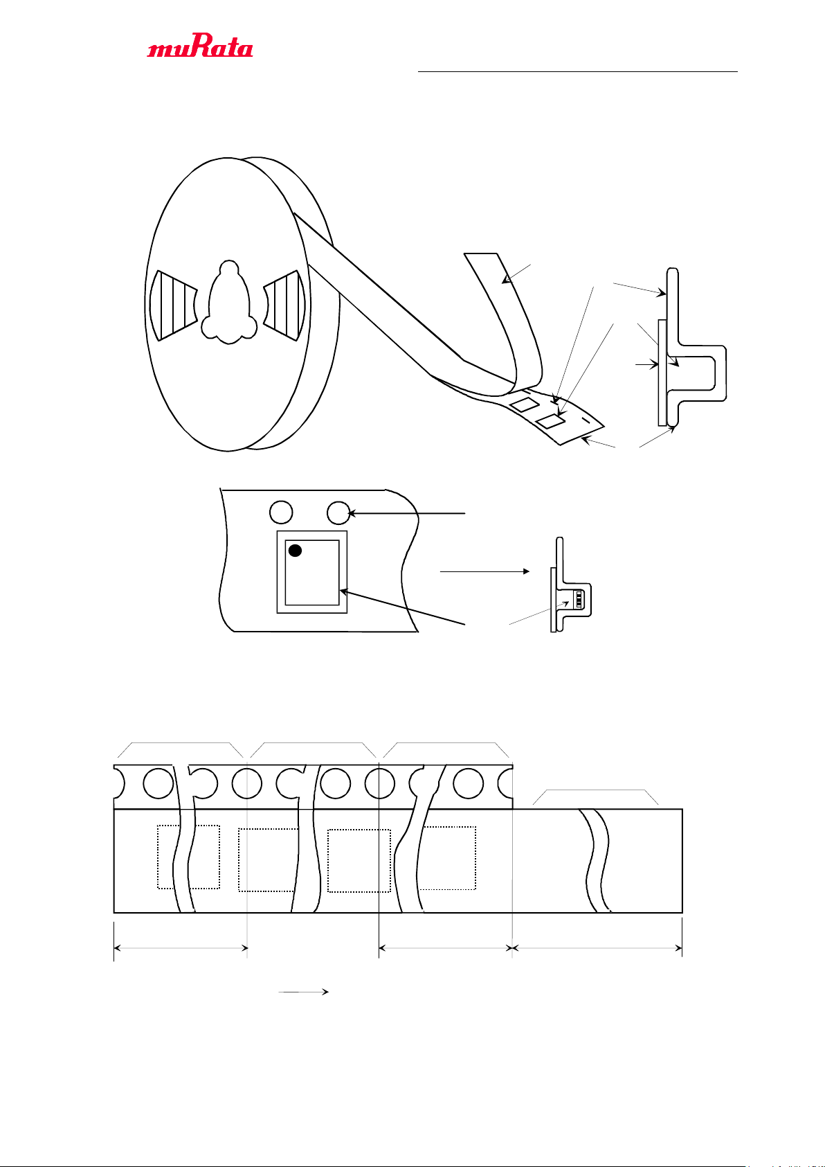
Feeding Hole
Chip
Feeding Direction
[2]
[3]
[4]
[3]
[1]
160 to 190 mm
Tail tape
(No components)
Components
No components
Feeding direction
Leader tape
(Cover tape alone)
150mm min.
250 mm min.
25 / 38
(3) Taping Diagrams
[1] Feeding Hole : As specified in (1)
[2] Hole for chip : As specified in (1)
[3] Cover tape : 62 um in thickness
[4] Base tape : As specified in (1)
(4) Leader and Tail tape
Preliminary & Confidential
< Specification may be changed by Murata without notice >
Murata(China) Investment Co., Ltd.
Page 27
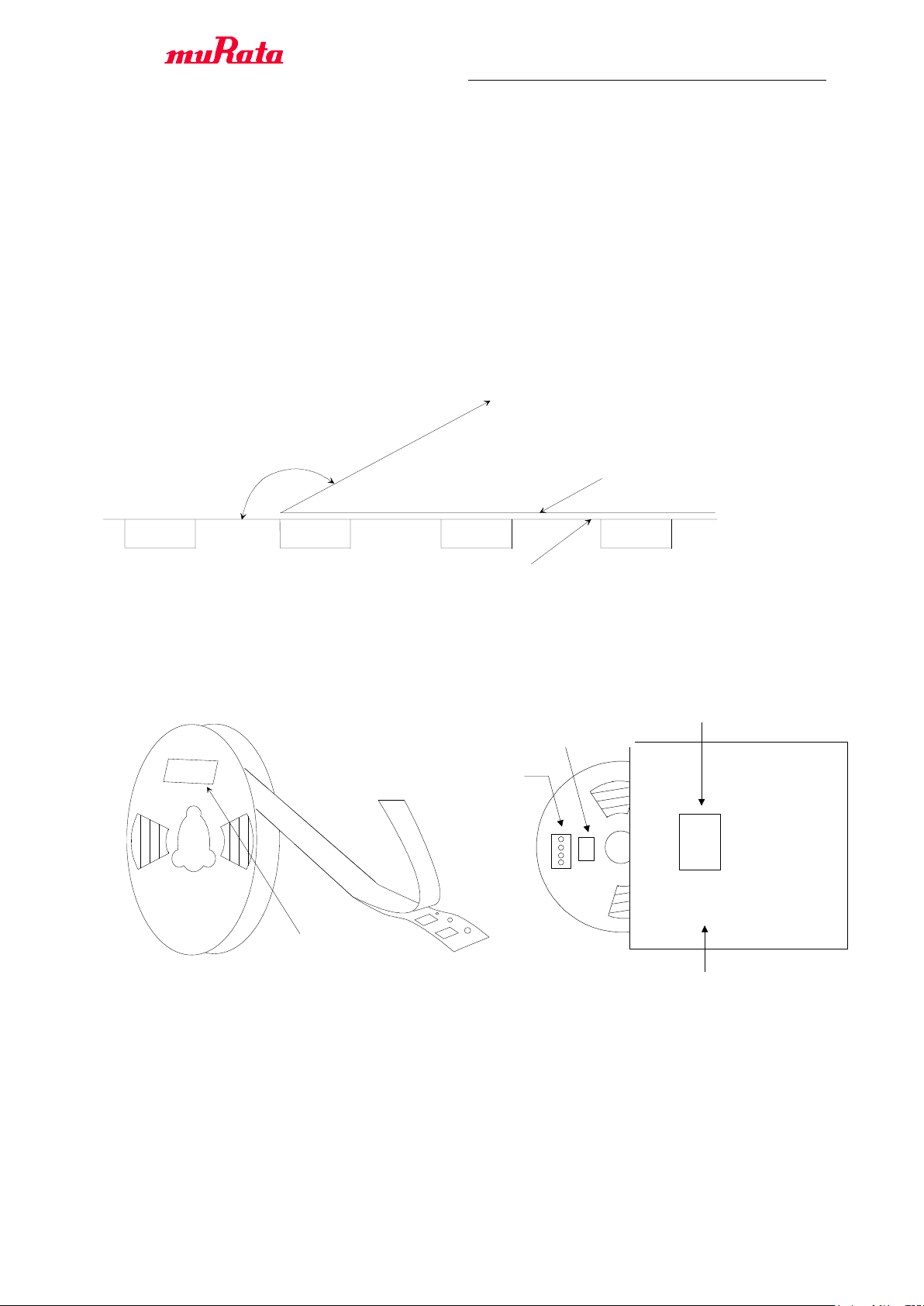
湿度
イ ン ジケ -タ
乾燥剤
表示ラ べル
防湿梱包袋
表示ラ ベル
Label
Label
Desiccant
Humidity
Indicator
Anti-humidity
Plastic Bag
165 to 180 °
1.1 N max.
Base tape
Cover tape
Preliminary Specification Number : SP-ZZ1PJ-F
26 / 38
-The tape for chips are wound clockwise, the feeding holes to the right side as the tape is pulled
toward the user.
-The cover tape and base tape are not adhered at no components area for 250 mm min.
-Tear off strength against pulling of cover tape: 5 N min.
-Packaging unit: 1000 pcs/ reel
- Material: Base tape: Plastic
Reel : Plastic
Cover tape, cavity tape and reel are made the anti-static processing.
- Peeling of force: 1.1 N max. in the direction of peeling as shown below.
- PACKAGE (Humidity proof packing)
Tape and reel must be sealed with the anti-humidity plastic bag. The bag contains the desiccant
and the humidity indicator.
Preliminary & Confidential
< Specification may be changed by Murata without notice >
Murata(China) Investment Co., Ltd.
Page 28

Preliminary Specification Number : SP-ZZ1PJ-F
27 / 38
18. NOTICE
18.1. Storage Conditions:
Please use this product within 6month after receipt.
- The product shall be stored without opening the packing under the ambient temperature from 5 to
35deg.C and humidity from 20 to 70%RH.
(Packing materials, in particular, may be deformed at the temperature over 40deg.C.)
- The product left more than 6months after reception, it needs to be confirmed the solderbility before
used.
- The product shall be stored in non corrosive gas (Cl2, NH3, SO2, Nox, etc.).
- Any excess mechanical shock including, but not limited to, sticking the packing materials by sharp
object and dropping the product, shall not be applied in order not to damage the packing materials.
This product is applicable to MSL3 (Based on JEDEC Standard J-STD-020)
- After the packing opened, the product shall be stored at <30deg.C / <60%RH and the product shall be
used within 168hours.
- When the color of the indicator in the packing changed, the product shall be baked before soldering.
Baking condition: 125+5/-0deg.C, 24hours, 1time
The products shall be baked on the heat-resistant tray because the material (Base Tape, Reel Tape and
Cover Tape) are not heat-resistant.
18.2. Handling Conditions:
Be careful in handling or transporting products because excessive stress or mechanical shock may
break products.
Handle with care if products may have cracks or damages on their terminals, the characteristics of
products may change. Do not touch products with bear hands that may result in poor solder ability and
destroy by static electrical charge.
18.3. Standard PCB Design (Land Pattern and Dimensions):
All the ground terminals should be connected to the ground patterns. Furthermore, the ground pattern
should be provided between IN and OUT terminals. Please refer to the specifications for the standard
land dimensions.
The recommended land pattern and dimensions is as Murata's standard. The characteristics of
products may vary depending on the pattern drawing method, grounding method, land dimensions,
land forming method of the NC terminals and the PCB material and thickness. Therefore, be sure to
verify the characteristics in the actual set. When using non-standard lands, contact Murata beforehand.
18.4. Notice for Chip Placer:
When placing products on the PCB, products may be stressed and broken by uneven forces from a
worn-out chucking locating claw or a suction nozzle. To prevent products from damages, be sure to
follow the specifications for the maintenance of the chip placer being used. For the positioning of
products on the PCB, be aware that mechanical chucking may damage products.
Preliminary & Confidential
< Specification may be changed by Murata without notice >
Murata(China) Investment Co., Ltd.
Page 29
Preliminary Specification Number : SP-ZZ1PJ-F
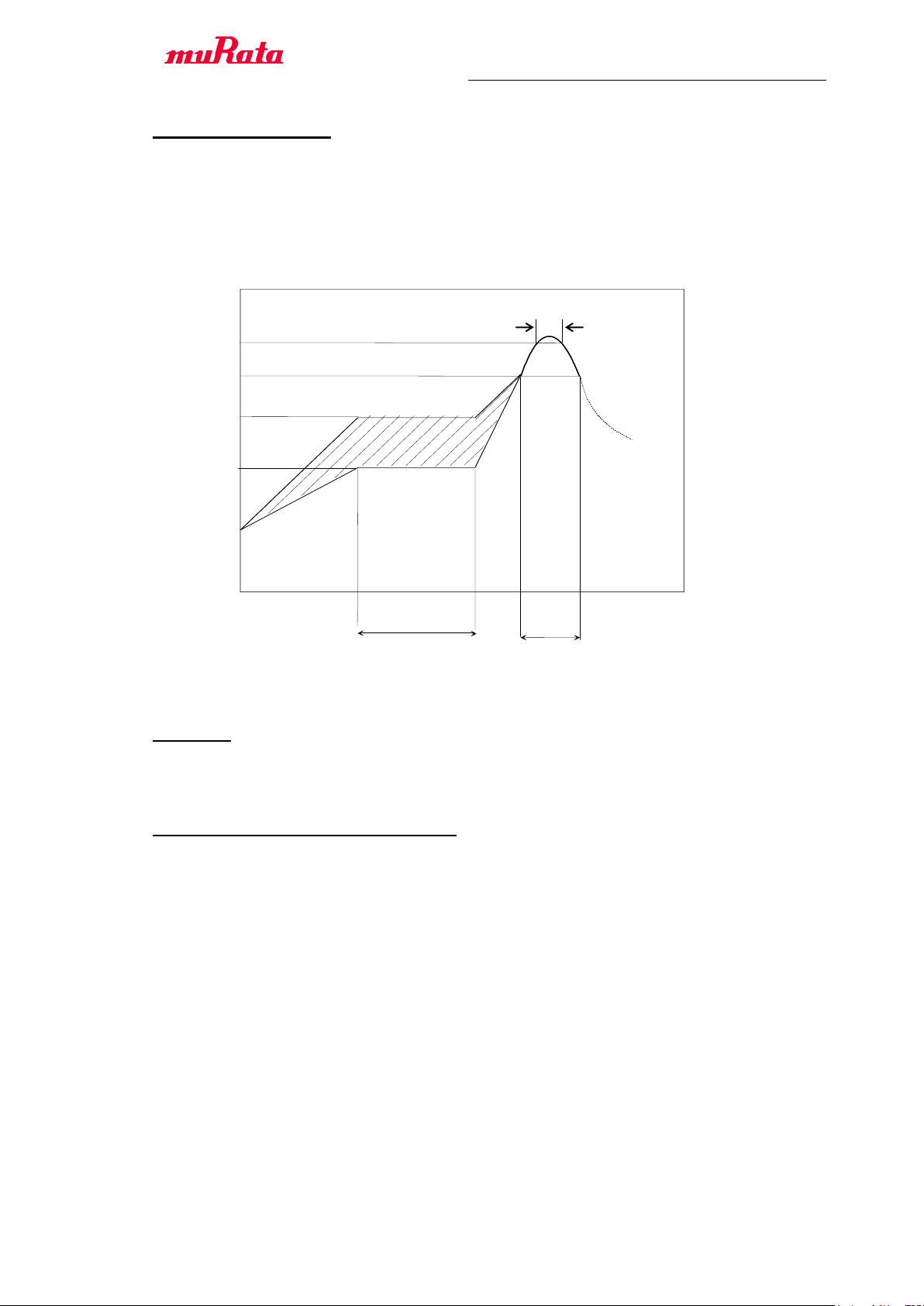
Within 120s
Pre-heating
time(s)
220 deg.C
Within 60s
Cooling down
Slowly
180 deg.C
150 deg.C
235 to 245 deg.C
Within 3s
28 / 38
18.5. Soldering Conditions:
The recommendation conditions of soldering are as in the following figure.
When products are immersed in solvent after mounting, pay special attention to maintain the
temperature difference within 100 °C. Soldering must be carried out by the above mentioned
conditions to prevent products from damage. Set up the highest temperature of reflow within 260 °C.
Contact Murata before use if concerning other soldering conditions.
Reflow soldering standard conditions(Example)
Please use the reflow within 2 times.
Use rosin type flux or weakly active flux with a chlorine content of 0.2 wt % or less.
18.6. Cleaning:
Since this Product is Moisture Sensitive, any cleaning is not permitted.
18.7. Operational Environment Conditions:
Products are designed to work for electronic products under normal environmental conditions (ambient
temperature, humidity and pressure). Therefore, products have no problems to be used under the
similar conditions to the above-mentioned. However, if products are used under the following
circumstances, it may damage products and leakage of electricity and abnormal temperature may
occur.
- In an atmosphere containing corrosive gas ( Cl2, NH3, SOx, NO
- In an atmosphere containing combustible and volatile gases.
- Dusty place.
- Direct sunlight place.
- Water splashing place.
- Humid place where water condenses.
- Freezing place.
If there are possibilities for products to be used under the preceding clause, consult with Murata before
actual use.
As it might be a cause of degradation or destruction to apply static electricity to products, do not apply
x
etc.).
Preliminary & Confidential
< Specification may be changed by Murata without notice >
Murata(China) Investment Co., Ltd.
Page 30

Preliminary Specification Number : SP-ZZ1PJ-F
29 / 38
static electricity or excessive voltage while assembling and measuring.
18.8. Input Power Capacity:
Products shall be used in the input power capacity as specified in this specifications.
Inform Murata beforehand, in case that the components are used beyond such input power capacity
range.
Preliminary & Confidential
< Specification may be changed by Murata without notice >
Murata(China) Investment Co., Ltd.
Page 31

Preliminary Specification Number : SP-ZZ1PJ-F
30 / 38
19. PRECONDITION TO USE OUR PRODUCTS
PLEASE READ THIS NOTICE BEFORE USING OUR PRODUCTS.
Please make sure that your product has been evaluated and confirmed from the aspect of the fitness for the
specifications of our product when our product is mounted to your product.
All the items and parameters in this product specification/datasheet/catalog have been prescribed on t he premise that
our product is used for the purpose, under the condition and in the environment specified in this specification. You are
requested not to use our product deviating from the condition and the environment specified in this specification.
Please note that the only warranty that we provide regarding the products is its conformance to the specifications
provided herein. Accordingly, we shall not be responsible for any defects in products or equipment incorporating such
products, which are caused under the conditions other than those specified in this specification.
WE HEREBY DISCLAIMS ALL OTHER WARRANTIES REGARDING THE PRODUCTS, EXPRESS OR IMPLIED,
INCLUDING WITHOUT LIMITATION ANY WARRANTY OF FITNESS FOR A PARTICULAR PURPOSE, THAT THEY
ARE DEFECT-FREE, OR AGAINST INFRINGEMENT OF INTELLECTUAL PROPERTY RIGHTS.
The product shall not be used in any application listed below which requires especially high reliability for the prevention
of such defect as may directly cause damage to the third party's life, body or property. You acknowledge and agree that,
if you use our products in such applications, we will not be responsible for any failure to meet such requirements.
Furthermore, YOU AGREE TO INDEMNIFY AND DEFEND US AND OUR AFFILIATES AGAINST ALL CLAIMS,
DAMAGES, COSTS, AND EXPENSES THAT MAY BE INCURRED, INCLUDING WITHOUT LIMITATION, ATTORNEY
FEES AND COSTS, DUE TO THE USE OF OUR PRODUCTS IN SUCH APPLICATIONS.
- Aircraft equipment. - Aerospace equipment - Undersea equipment.
- Power plant control equipment - Medical equipment.
- Transportation equipment (vehicles, trains, ships, elevator, etc.).
- Traffic signal equipment. - Disaster prevention / crime prevention equipment.
-Burning / explosion control equipment
- Application of similar complexity and/ or reliability requirements to the applications listed in the above.
We expressly prohibit you from analyzing, breaking, reverse-engineering, remodeling altering, and reproducing our
product. Our product cannot be used for the product which is prohibited from being manufactured, used, and sold by
the regulations and laws in the world.
We do not warrant or represent that any license, either express or implied, is granted under any our patent right,
copyright, mask work right, or our other intellectual property right relating to any combination, machine, or process in
which our products or services are used. Information provided by us regarding third-party products or services does not
constitute a license from us to use such products or services or a warranty or endorsement thereof. Use of such
information may require a license from a third party under the patents or other intellectual property of the third party, or a
license from us under our patents or other intellectual property.
Please do not use our products, our technical information and other data provided by us for the purpose of developing of
mass-destruction weapons and the purpose of military use.
Moreover, you must comply with "foreign exchange and foreign trade law", the "U.S. export administration regulations",
etc.
Please note that we may discontinue the manufacture of our products, due to reasons such as end of supply of materials
and/or components from our suppliers.
By signing on specification sheet or approval sheet, you acknowledge that you are the legal representative for your
company and that you understand and accept the validity of the contents herein. When you are not able to return the
signed version of specification sheet or approval sheet within 30 days from receiving date of specification sheet or
approval sheet, it shall be deemed to be your consent on the content of specification sheet or approval sheet. Customer
acknowledges that engineering samples may deviate from specifications and may contain defects due to their
development status. We reject any liability or product warranty for engineering samples. In particular we disclaim liability
for damages caused by
- the use of the engineering sample other than for evaluation purposes, particularly the installation or integration in the
product to be sold by you,
-deviation or lapse in function of engineering sample,
-improper use of engineering samples.
We disclaim any liability for consequential and incidental damages.
If you can’t agree the above contents, you should inquire our sales.
Preliminary & Confidential
< Specification may be changed by Murata without notice >
Murata(China) Investment Co., Ltd.
Page 32

Appendix
Preliminary Specification Number : SP-ZZ1PJ-F
31 / 38
Preliminary & Confidential
< Specification may be changed by Murata without notice >
Murata(China) Investment Co., Ltd.
Page 33
Preliminary Specification Number : SP-ZZ1PJ-F
FCC ID:
VPYLB1PJ
Frequency of operation
Scan
Ad-hoc
mode
2.4GHz
802.11b/g/n-HT20
2412MHz – 2462MHz (ch1 – ch11)
Active
Yes
802.11n-HT40
2422MHz – 2452MHz (ch3 – ch9)
Active
Yes
W52
802.11a/n-HT20/ac-VHT-20
5180MHz – 5240MHz (ch36 – ch48)
Active
Yes
802.11n-HT40/ac-VHT-40
5190MHz – 5239MHz (ch38 – ch46)
Active
Yes
802.11ac-VHT80
5210MHz (ch42)
Active
Yes
W53
802.11a/n-HT20/ac-VHT-20
5260MHz – 5320MHz (ch52 – ch64)
Passive
No
802.11n-HT40/ac-VHT-40
5270MHz – 5310MHz (ch54 – ch62)
Passive
No
802.11ac-VHT80
5290MHz (ch58)
Passive
No
W56
802.11a/n-HT20/ac-VHT-20
5500MHz – 5720MHz (ch100 – ch144)
Passive
No
802.11n-HT40/ac-VHT-40
5510MHz – 5710MHz (ch102 – ch142)
Passive
No
802.11ac-VHT80
5530MHz – 5690MHz (ch106 – ch138)
Passive
No
W58
802.11a/n-HT20/ac-VHT-20
5745MHz – 5825MHz (ch149 – ch165)
Active
Yes
802.11n-HT40/ac-VHT-40
5755MHz – 5795MHz (ch151 – ch159)
Active
Yes
802.11ac-VHT80
5775MH (ch155)
Active
Yes
32 / 38
LBEE5ZZ1PJ Installation Manual (FCC)
FCC ID of this module is as follows;
For OEM integration only – device cannot be sold to general public.
Therefore we will ask OEM to include the following statement required by FCC on the product and in
the installation manual Notice.
Contents
1. Theory of operation
2. Antenna
3. Notice
1. Theory of operation
The device cannot operate in 5600MHz~5650MHz band in Canada
Compliance with FCC requirement 15.407(c)
Data transmission is always initiated by software, which is the passed down through the MAC, through
the digital and analog baseband, and finally to the RF chip. Several special packets are initiated by the
MAC. These are the only ways the digital baseband portion will turn on the RF transmitter, which it then
turns off at the end of the packet. Therefore, the transmitter will be on only while one of the
aforementioned packets is being transmitted. In other words, this device automatically discontinue
transmission in case of either absence of information to transmit or operational failure.
Frequency Tolerance: ± 20ppm
End users cannot modify the software because F/W & driver are installed in device.
< Specification may be changed by Murata without notice >
Preliminary & Confidential
Murata(China) Investment Co., Ltd.
Page 34
Preliminary Specification Number : SP-ZZ1PJ-F
Antenna
Antenna type
PCB Antenna
50-ohm feed line length
We test it at 26.4mm as a representative
This device complies with part 15 of the FCC Rules. Operation is subject to the following two
conditions: (1) This device may not cause harmful interference, and (2) this device must accept any
interference received, including interference that may cause undesired operation.
FCC CAUTION
Changes or modifications not expressly approved by the party responsible for compliance could void
the user’s authority to operate the equipment.
This transmitter must not be co-located or operated in conjunction with any other antenna or
transmitter.
33 / 38
2. Antenna
■Please refer to KDB 996369
■Please perform the antenna design that followed the specifications of the antenna.
■About the signal line between an antenna and a module
It is a 50-ohm line design.
Fine tuning of return loss etc. can be performed using a matching network.
However, it is required to check "Class1 change" and "Class2 change" which the authorities define
then.
The concrete contents of a check are the following three points.
1) It is the same type as the antenna type of antenna specifications.
2) An antenna gain is lower than a gain given in antenna specifications.
3) The emission level is not getting worse.
■50-ohm feed line(microstrip line length)
3. Notice
For OEM integration only – device cannot be sold to general public.
Therefore we will ask OEM to include the following statements required by FCC/IC on the product and
in the Installation manual Notice.
Please describe the following warning on the final product which contains this module.
Contains Transmitter Module FCC ID: VPYLB1PJ
or
Contains FCC ID: VPYLB1PJ
●Please describe the following warning to the manual.
※When the product is small, as for these words mentioned above, the posting to a manual is possible.
●When installing it in a mobile equipment. Please describe the following warning to the manual.
This equipment complies with FCC radiation exposure limits set forth for an uncontrolled environment
and meets the FCC radio frequency (RF) Exposure Guidelines. This equipment should be installed and
operated keeping the radiator at least 20cm or more away from person’s body.
RF Exposure requirements are met when installed in mobile equipment.
This module cannot be installed in portable equipment without further testing and a change to FCC's
grant of authorization. Contact Murata regarding portable applications.
Note)
Portable equipment : Equipment for which the spaces between human body and antenna are used
within 20cm.
Mobile equipment : Equipment used at position in which the spaces between human body and antenna
exceeded 20cm.
Preliminary & Confidential
< Specification may be changed by Murata without notice >
Murata(China) Investment Co., Ltd.
Page 35

Preliminary Specification Number : SP-ZZ1PJ-F
34 / 38
This device is intended only for OEM integrators under the following conditions:
1) The antenna must be installed such that 20 cm is maintained between the antenna and users, and
2) The transmitter module may not be co-located with any other transmitter or antenna.
3) The use of an antenna with gain less than 3.1 dBi(2.4GHz) and 2.8 dBi(5GHz).
As long as 3 conditions above are met, further transmitter test will not be required. However, the OEM
integrator is still responsible for testing their end-product for any additional compliance requirements
required with this module installed
IMPORTANT NOTE: In the event that these conditions cannot be met (for example certain laptop
configurations or co-location with another transmitter), then the FCC authorization is no longer
considered valid and the FCC ID cannot be used on the final product. In these circumstances, the OEM
integrator will be responsible for re-evaluating the end product (including the transmitter) and obtaining
a separate FCC authorization.
End Product Labeling
This transmitter module is authorized only for use in device where the antenna may be installed such
that 20 cm may be maintained between the antenna and users. The final end product must be labeled
in a visible area with the following: “Contains FCC ID: VPYLB1PJ ”. The grantee's FCC ID can be used
only when all FCC compliance requirements are met.
Manual Information To the End User
The OEM integrator has to be aware not to provide information to the end user regarding how to install
or remove this RF module in the user’s manual of the end product which integrates this module.
The end user manual shall include all required regulatory information/warning as show in this manual.
Note: This equipment has been tested and found to comply with the limits for a Class B digital device,
pursuant to part 15 of the FCC Rules. These limits are designed to provide reasonable protection
against harmful interference in a residential installation. This equipment generates, uses and can
radiate radio frequency energy and, if not installed and used in accordance with the instructions, may
cause harmful interference to radio communications. However, there is no guarantee that interference
will not occur in a particular installation. If this equipment does cause harmful interference to radio or
television reception, which can be determined by turning the equipment off and on, the user is
encouraged to try to correct the interference by one or more of the following measures:
—Reorient or relocate the receiving antenna.
—Increase the separation between the equipment and receiver.
—Connect the equipment into an outlet on a circuit different from that to which the receiver is connected.
—Consult the dealer or an experienced radio/TV technician for help.
Preliminary & Confidential
< Specification may be changed by Murata without notice >
Murata(China) Investment Co., Ltd.
Page 36
Preliminary Specification Number : SP-ZZ1PJ-F
IC:
772C-LB1PJ
Frequency of operation
Scan
Ad-hoc
mode
2.4GHz
802.11b/g/n-HT20
2412MHz – 2462MHz (ch1 – ch11)
Active
Yes
802.11n-HT40
2422MHz – 2452MHz (ch3 – ch9)
Active
Yes
W52
802.11a/n-HT20/ac-VHT-20
5180MHz – 5240MHz (ch36 – ch48)
Active
Yes
802.11n-HT40/ac-VHT-40
5190MHz – 5239MHz (ch38 – ch46)
Active
Yes
802.11ac-VHT80
5210MHz (ch42)
Active
Yes
W53
802.11a/n-HT20/ac-VHT-20
5260MHz – 5320MHz (ch52 – ch64)
Passive
No
802.11n-HT40/ac-VHT-40
5270MHz – 5310MHz (ch54 – ch62)
Passive
No
802.11ac-VHT80
5290MHz (ch58)
Passive
No
W56
802.11a/n-HT20/ac-VHT-20
5500MHz – 5720MHz (ch100 – ch144)
Passive
No
802.11n-HT40/ac-VHT-40
5510MHz – 5710MHz (ch102 – ch142)
Passive
No
802.11ac-VHT80
5530MHz – 5690MHz (ch106 – ch138)
Passive
No
W58
802.11a/n-HT20/ac-VHT-20
5745MHz – 5825MHz (ch149 – ch165)
Active
Yes
802.11n-HT40/ac-VHT-40
5755MHz – 5795MHz (ch151 – ch159)
Active
Yes
802.11ac-VHT80
5775MH (ch155)
Active
Yes
35 / 38
LBEE5ZZ1PJ Installation Manual (IC)
IC No. of this device is as follows;
For OEM integration only – device cannot be sold to general public.
Therefore, we will ask OEM to include the following statements required by IC on the product and in the
installation manual Notice.
Contents
1. Theory of operation
2. Antenna
3. Notice
1. Theory of operation
The device cannot operate in 5600MHz~5650MHz band in Canada
Data transmission is always initiated by software, which is the passed down through the MAC, through
the digital and analog baseband, and finally to the RF chip. Several special packets are initiated by the
MAC. These are the only ways the digital baseband portion will turn on the RF transmitter, which it then
turns off at the end of the packet. Therefore, the transmitter will be on only while one of the
aforementioned packets is being transmitted. In other words, this device automatically discontinue
transmission in case of either absence of information to transmit or operational failure.
La transmission des données est toujours initiée par le logiciel, puis les données sont transmises par
'intermédiaire du MAC, par la bande de base numérique et analogique et, enfin, à la puce RF. Plusieurs
paquets spéciaux sont initiés par le MAC. Ce sont les seuls moyens pour qu'une partie de la bande de
base numérique active l'émetteur RF, puis désactive celui-ci à la fin du paquet. En conséquence,
l'émetteur reste uniquement activé lors de la transmission d'un des paquets susmentionnés. En
d'autres termes, ce dispositif interrompt automatiquement toute transmission en cas d'absence
d'information à transmettre ou de défaillance.
End users cannot modify the software because F/W & driver are installed in device.
< Specification may be changed by Murata without notice >
Preliminary & Confidential
Murata(China) Investment Co., Ltd.
Page 37
Preliminary Specification Number : SP-ZZ1PJ-F
Antenna
Antenna type
PCB Antenna
50-ohm feed line length
We test it at 26.4mm as a representative
5150-5250 MHz band is restricted to indoor operation only.
La bande 5150-5250 MHz est restreinte à une utilisation à l’intérieur seulement.
High-power radars are allocated as primary users (i.e. priority users) of the bands 5250-5350 MHz and
5650-5850
MHz and that these radars could cause interference and/or damage to LE-LAN devices.
Les radars de haute puissance sont désignés utilisateurs principaux (c.-à-d., qu'ils ont la priorité) pour les
bandes 5250-5350 MHz et 5650-5850 MHz, et ces radars pourraient causer du brouillage et/ou des
dommages aux dispositifs LAN-EL.
36 / 38
2. Antenna
■Please refer to KDB 996369
■Please perform the antenna design that followed the specifications of the antenna.
■About the signal line between an antenna and a module
It is a 50-ohm line design.
Fine tuning of return loss etc. can be performed using a matching network.
However, it is required to check "Class1 change" and "Class2 change" which the authorities define
then.
The concrete contents of a check are the following three points.
1) It is the same type as the antenna type of antenna specifications.
2) An antenna gain is lower than a gain given in antenna specifications.
3) The emission level is not getting worse.
■50-ohm feed line(microstrip line length)
3. Notice
For OEM integration only – device cannot be sold to general public.
Therefore we will ask OEM to include the following statements required by FCC/IC on the product and in the
Installation manual Notice.
Please describe the following warning on the final product which contains this module.
Contains IC: 772C-LB1PJ
This device complies with Industry Canada’s licence-exempt RSSs. Operation is subject to the
following two conditions:
(1) This device may not cause interference; and
(2) This device must accept any interference, including interference that may cause undesired
operation of the device.
Le présent appareil est conforme aux CNR d’Industrie Canada applicables aux appareils radio exempts
de licence.
L’exploitation est autorisée aux deux conditions suivantes :
1) l’appareil ne doit pas produire de brouillage;
2) l’utilisateur de l’appareil doit accepter tout brouillage radioélectrique subi, même si le brouillage est
susceptible d’en compromettre le fonctionnement.
*When the product is small, as for these words mentioned above, the posting to a manual is possible.
Preliminary & Confidential
< Specification may be changed by Murata without notice >
Murata(China) Investment Co., Ltd.
Page 38

Preliminary Specification Number : SP-ZZ1PJ-F
This equipment complies with IC radiation exposure limits set forth for an uncontrolled environment and
meets RSS-102 of the IC radio frequency (RF) Exposure rules. This equipment should be installed and
operated keeping the radiator at least 20cm or more away from person’s body.
Cet équipement est conforme aux limites d’exposition aux rayonnements énoncées pour un environnement
non contrôlé et respecte les règles d’exposition aux fréquences radioélectriques (RF) CNR-102 de l’IC. Cet
équipement doit être installé et utilisé en gardant une distance de 20 cm ou plus entre le radiateur et le corps
humain.
37 / 38
●When installing it in a mobile equipment. Please describe the following warning to the manual.
RF Exposure requirements are met when installed in mobile equipment.
This module cannot be installed in portable equipment without further testing and a change to FCC's grant of
authorization.
Contact Murata regarding portable applications.
Note)
Portable equipment : Equipment for which the spaces between human body and antenna are used within
20cm.
Mobile equipment : Equipment used at position in which the spaces between human body and antenna
exceeded 20cm.
This device is intended only for OEM integrators under the following conditions: (For module
device use)
1) The antenna must be installed such that 20 cm is maintained between the antenna and users, and
2) The transmitter module may not be co-located with any other transmitter or antenna.
3)The use of an antenna with gain less than 3.1 dBi(2.4GHz) and 2.8 dBi(5GHz).
As long as 3 conditions above are met, further transmitter test will not be required. However, the OEM
integrator is still responsible for testing their end-product for any additional compliance requirements
required with this module installed.
Cet appareil est conçu uniquement pour les intégrateurs OEM dans les conditions suivantes:
(Pour utilisation de dispositif module)
1)L'antenne doit être installée de telle sorte qu'une distance de 20 cm est respectée entre l'antenne et
les utilisateurs, et
2)Le module émetteur peut ne pas être coïmplanté avec un autre émetteur ou antenne.
Tant que les 3 conditions ci-dessus sont remplies, des essais supplémentaires sur l'émetteur ne seront pas
nécessaires. Toutefois, l'intégrateur OEM est toujours responsable des essais sur son produit final pour
toutes exigences de conformité supplémentaires requis pour ce module installé.
Data transmission is always initiated by software, which is the passed down through the MAC, through
the digital and analog baseband, and finally to the RF chip. Several special packets are initiated by the
MAC. These are the only ways the digital baseband portion will turn on the RF transmitter, which it then
turns off at the end of the packet. Therefore, the transmitter will be on only while one of the
aforementioned packets is being transmitted. In other words, this device automatically discontinue
transmission in case of either absence of information to transmit or operational failure.
La transmission des données est toujours initiée par le logiciel, puis les données sont transmises par
'intermédiaire du MAC, par la bande de base numérique et analogique et, enfin, à la puce RF. Plusieurs
paquets spéciaux sont initiés par le MAC. Ce sont les seuls moyens pour qu'une partie de la bande de
base numérique active l'émetteur RF, puis désactive celui-ci à la fin du paquet. En conséquence,
l'émetteur reste uniquement activé lors de la transmission d'un des paquets susmentionnés. En
d'autres termes, ce dispositif interrompt automatiquement toute transmission en cas d'absence
d'information à transmettre ou de défaillance.
Preliminary & Confidential
< Specification may be changed by Murata without notice >
Murata(China) Investment Co., Ltd.
Page 39

Preliminary Specification Number : SP-ZZ1PJ-F
38 / 38
IMPORTANT NOTE:
In the event that these conditions cannot be met (for example certain laptop configurations or
co-location with another transmitter), then the Canada authorization is no longer considered valid and
the IC ID cannot be used on the final product. In these circumstances, the OEM integrator will be
responsible for re-evaluating the end product (including the transmitter) and obtaining a separate
Canada authorization.
NOTE IMPORTANTE:
Dans le cas où ces conditions ne peuvent être satisfaites (par exemple pour certaines configurations
d'ordinateur portable ou de certaines co-localisation avec un autre émetteur), l'autorisation du Canada
n'est plus considéré comme valide et l'ID IC ne peut pas être utilisé sur le produit final. Dans ces
circonstances, l'intégrateur OEM sera chargé de réévaluer le produit final (y compris l'émetteur) et
'obtention d'une autorisation distincte au Canada.
End Product Labeling
This transmitter module is authorized only for use in device where the antenna may be installed such
that 20 cm may be maintained between the antenna and users. The final end product must be labeled
in a visible area with the following: “Contains IC: 772C-LB1PJ ”.
Plaque signalétique du produit final
Ce module émetteur est autorisé uniquement pour une utilisation dans un dispositif où l'antenne peut
être installée de telle sorte qu'une distance de 20cm peut être maintenue entre l'antenne et les
utilisateurs. Le produit final doit être étiqueté dans un endroit visible avec l'inscription suivante:
"Contient des IC: 772C-LB1PJ ".
Manual Information To the End User
The OEM integrator has to be aware not to provide information to the end user regarding how to install
or remove this RF module in the user’s manual of the end product which integrates this module.
The end user manual shall include all required regulatory information/warning as show in this manual.
Manuel d'information à l'utilisateur final
L'intégrateur OEM doit être conscient de ne pas fournir des informations à l'utilisateur final quant à la
façon d'installer ou de supprimer ce module RF dans le manuel de l'utilisateur du produit final qui
intègre ce module.
Le manuel de l'utilisateur final doit inclure toutes les informations réglementaires requises et
avertissements comme indiqué dans ce manuel.
Preliminary & Confidential
< Specification may be changed by Murata without notice >
Murata(China) Investment Co., Ltd.
 Loading...